navdeep kaur presentation
TRANSCRIPT
8/2/2019 Navdeep Kaur Presentation
http://slidepdf.com/reader/full/navdeep-kaur-presentation 1/37

8/2/2019 Navdeep Kaur Presentation
http://slidepdf.com/reader/full/navdeep-kaur-presentation 2/37
Nanomaterials is a field that takes a materialscience based approach to nanotechnology
It studies materials with morphologicalfeatures on the nanoscale, and especiallythose that have special properties stemmingfrom their nanoscale dimensions.
Nanoscale is usually defined as smaller than a
one tenth of a micrometer in at least onedimension.
8/2/2019 Navdeep Kaur Presentation
http://slidepdf.com/reader/full/navdeep-kaur-presentation 3/37
1.Fullerenes
2.Nanoparticles
The fullerenes are a class of allotropes of
carbon which conceptually are graphenesheets rolled into tubes or spheres. Theseinclude the carbon nanotubes (or siliconnanotubes) which are of interest both
because of their mechanical strength and alsobecause of their electrical properties.

8/2/2019 Navdeep Kaur Presentation
http://slidepdf.com/reader/full/navdeep-kaur-presentation 4/37
Nanoparticles or nanocrystals made of metals, semiconductors, or oxides are of particular interest for their mechanical,electrical, magnetic, optical, chemical and
other properties. Nanoparticles have beenused as quantum dots and as chemicalcatalysts.
8/2/2019 Navdeep Kaur Presentation
http://slidepdf.com/reader/full/navdeep-kaur-presentation 5/37
Top-down approach
Bottom-up approach

8/2/2019 Navdeep Kaur Presentation
http://slidepdf.com/reader/full/navdeep-kaur-presentation 6/37
Uses thetraditionalmethods to
pattern abulk waferas in EE 418lab.
Is limited bytheresolution of lIthography.
http

8/2/2019 Navdeep Kaur Presentation
http://slidepdf.com/reader/full/navdeep-kaur-presentation 7/37
Adding a layer of material over theentire wafer andpatterning thatlayer throughphotolithography.
Patterning bulk
silicon by etchingaway certainareas.
8/2/2019 Navdeep Kaur Presentation
http://slidepdf.com/reader/full/navdeep-kaur-presentation 8/37
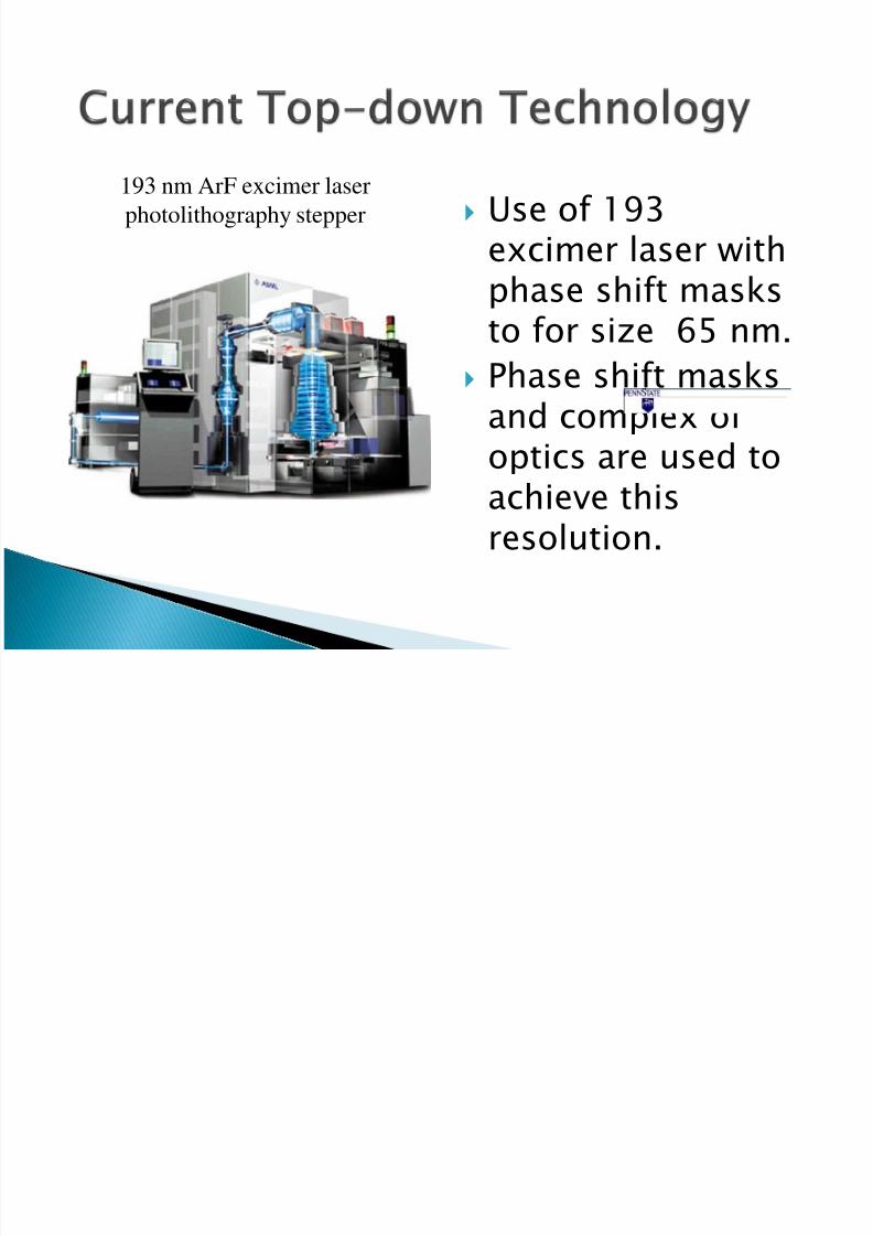
Use of 193excimer laser with
phase shift masksto for size 65 nm.
Phase shift masksand complex of
optics are used toachieve thisresolution.
193 nm ArF excimer laser
photolithography stepper

8/2/2019 Navdeep Kaur Presentation
http://slidepdf.com/reader/full/navdeep-kaur-presentation 9/37
Cost of new machinesand clean roomenvironments growsexponentially with
newer technologies. Physical limits of
photolithography arebecoming a problem.
With smallergeometries andconventional materials,heat dissipation is aproblem.

8/2/2019 Navdeep Kaur Presentation
http://slidepdf.com/reader/full/navdeep-kaur-presentation 10/37
The opposite of thetop-downapproach.
Instead of takingmaterial away tomake structures,the bottom-upapproach selectivelyadds atoms tocreate structures.

8/2/2019 Navdeep Kaur Presentation
http://slidepdf.com/reader/full/navdeep-kaur-presentation 11/37
Nature uses thebottom upapproach.◦ Cells◦ Crystals◦ Humans
Chemistry and
biology can helpto assemble andcontrol growth.

8/2/2019 Navdeep Kaur Presentation
http://slidepdf.com/reader/full/navdeep-kaur-presentation 12/37
Etched wafer with
desired pattern
Apply layer of
photoresist
Expose wafer with UV
light through mask and
etch wafer
Start with bulk wafer
Top Down Process Bottom Up Process
Start with bulk wafer
Alter area of wafer wherestructure is to be created by
adding polymer or seed
crystals or other
techniques.
Grow or assemble the
structure on the area
determined by the seed
crystals or polymer.
(self assembly)
Similar results can be obtained through bottom-up and top-down processes

8/2/2019 Navdeep Kaur Presentation
http://slidepdf.com/reader/full/navdeep-kaur-presentation 13/37
Allows smaller geometries thanphotolithography.
Certain structures such as CarbonNanotubes and Si nanowires are grown
through a bottom-up process. New technologies such as organicsemiconductors employ bottom-upprocesses to pattern them.
Can make formation of films and structures
much easier. Is more economical than top-down in that it
does not waste material to etching.

8/2/2019 Navdeep Kaur Presentation
http://slidepdf.com/reader/full/navdeep-kaur-presentation 14/37
The principle behind bottom-up processing. Self assembly is the coordinated action of
independent entities to produce larger,ordered structures or achieve a desiredshape.
Found in nature.
Start on the atomic scale.

8/2/2019 Navdeep Kaur Presentation
http://slidepdf.com/reader/full/navdeep-kaur-presentation 15/37
Self-organizingdeposition of siliconnanodots.
Formation of Nanowires.
Nanotube transistor.
Self-assembled
monolayers. Carbon nanotube
interconnects.

8/2/2019 Navdeep Kaur Presentation
http://slidepdf.com/reader/full/navdeep-kaur-presentation 16/37
Most commonapplications are inoptical devices andmemory.
Silicon nanodots aredeposited ontosilicon dioxide withno need forlithographicpatterning.

8/2/2019 Navdeep Kaur Presentation
http://slidepdf.com/reader/full/navdeep-kaur-presentation 17/37
Process for makingnanodots
1. Apply layer of self-assembledpolymer film.
2. Grow layer of
desired materialto createnanodot.
Polymer template for nanodot
65 billion nanodots per square cm

8/2/2019 Navdeep Kaur Presentation
http://slidepdf.com/reader/full/navdeep-kaur-presentation 18/37
Each nanodot can
hold one bit of
information.
10 Trillion dotsper square inch.
13 nm high
80 nm wide
Self Assembled Nanodots

8/2/2019 Navdeep Kaur Presentation
http://slidepdf.com/reader/full/navdeep-kaur-presentation 19/37
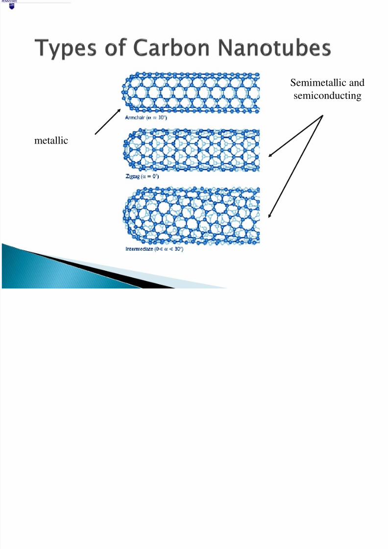
Stronger than steel Multiple tubes slide
inside of each otherwith minimal effects of
friction. Electrical current
density 1000 timesgreater than silver orcopper.
Can range from havingmetallic properties tosemiconductorproperties based on it’sconfiguration.
8/2/2019 Navdeep Kaur Presentation
http://slidepdf.com/reader/full/navdeep-kaur-presentation 20/37
metallic
Semimetallic and
semiconducting

8/2/2019 Navdeep Kaur Presentation
http://slidepdf.com/reader/full/navdeep-kaur-presentation 21/37
Deposit few particles of Iron (most common) toact as catalyst.
Apply a hot environment
of carbon containing gas(typically CH4) The particle catalyzes the
decomposition of the gasand carbon dissolves inthe particle.
When the particle issupersaturated withcarbon, it extrudes theexcess carbon in the formof a tube.

8/2/2019 Navdeep Kaur Presentation
http://slidepdf.com/reader/full/navdeep-kaur-presentation 22/37
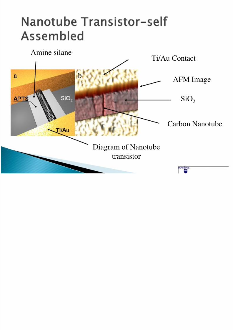
Basic diagram for ananotube transistor
Benefits of transistor
over conventionaldesigns:◦ Smaller◦ Faster
◦ Less material used
◦
Many of the problemsassociated withconventional devicesare solved
8/2/2019 Navdeep Kaur Presentation
http://slidepdf.com/reader/full/navdeep-kaur-presentation 23/37
Diagram of Nanotube
transistor
Carbon Nanotube
SiO2
Ti/Au Contact
AFM Image
Amine silane

8/2/2019 Navdeep Kaur Presentation
http://slidepdf.com/reader/full/navdeep-kaur-presentation 24/37
DNA strands connectto gold electrodes ontop of silicon.
DNA strands connectto ends of carbonnanotube.
Silicon and nanotubesare mixed and the
DNA makes theconnections to formnanotube transistors.
http://www.trnmag.com/Photos/2004/12150
4/DNA%20makes%20nanotube%20transist
ors%20Image.html

8/2/2019 Navdeep Kaur Presentation
http://slidepdf.com/reader/full/navdeep-kaur-presentation 25/37
Interface between metalelectrodes and carbonnanotube is verysensitive.
Changing just oneatom can significantlyaffect transistorperformance.
Self-assemblingnanotubes is not
efficient. Growing nanotubes in
place has had littlesuccess.

8/2/2019 Navdeep Kaur Presentation
http://slidepdf.com/reader/full/navdeep-kaur-presentation 26/37
Molecules aredepositedmolecule-by-
molecule to form aself-assembledmonolayer.
Creates a highquality layer of
material. Layers aredeposited one layerat a time.

8/2/2019 Navdeep Kaur Presentation
http://slidepdf.com/reader/full/navdeep-kaur-presentation 27/37
Organic moleculescan’t be depositedusing extremeconditions because it
would damage theorganic molecules. SAMS technique does
not damage organicmolecules.
SAMS films are nearly
defect free. Used to deposit organic
semiconductors.

8/2/2019 Navdeep Kaur Presentation
http://slidepdf.com/reader/full/navdeep-kaur-presentation 28/37
Metal contact actsas a catalyst topromote one-dimensionalcrystal growth.
Can one day be
implemented asinterconnects.
Silicon Nanowire Diameter <1nm

8/2/2019 Navdeep Kaur Presentation
http://slidepdf.com/reader/full/navdeep-kaur-presentation 29/37

8/2/2019 Navdeep Kaur Presentation
http://slidepdf.com/reader/full/navdeep-kaur-presentation 30/37
Can have a muchgreater conductivitythan copper.
Is more heat resistant
than copper. Carries a much larger
current than copper. Orientation of carbon
nanotubes remains aproblem.
Technology is notreliable enough to beused in devicemanufacturing.
Carbon nanotubes
grown on a metal
contact through
PECVD.
Carbon nanotubes after
layer of silicon dioxide
added.

8/2/2019 Navdeep Kaur Presentation
http://slidepdf.com/reader/full/navdeep-kaur-presentation 31/37
Making sure that the structures grow andassemble in the correct way.
Forming complex patterns and structuresusing self assembly.
Contamination has a significant impact ondevices with such small geometries.
Fabricating robust structures.

8/2/2019 Navdeep Kaur Presentation
http://slidepdf.com/reader/full/navdeep-kaur-presentation 32/37
Combination of top-down andbottom-up
processes tosimplifyconstruction.
Use catalysts andstresses to achievemore one-directional growth.

8/2/2019 Navdeep Kaur Presentation
http://slidepdf.com/reader/full/navdeep-kaur-presentation 33/37

8/2/2019 Navdeep Kaur Presentation
http://slidepdf.com/reader/full/navdeep-kaur-presentation 34/37
Carbon nanotubetransistor (StanfordU.)
Organic monolayersfor organic transistor(Yale U.)
Nanotube basedcircuit constructed
(IBM) Nanomotors and
gears created (NASA)

8/2/2019 Navdeep Kaur Presentation
http://slidepdf.com/reader/full/navdeep-kaur-presentation 35/37
Vias and interconnectsbeing implemented withcarbon nanotubes.
Nanotube transistors
replacing conventionaldesigns.
SAMS being used tocreate organicsemiconductor baseddevices.
Carbon nanotubesbecoming more and moreprevalent as their growthis controlled.
Nanotube array possibly used in
future televisions.

8/2/2019 Navdeep Kaur Presentation
http://slidepdf.com/reader/full/navdeep-kaur-presentation 36/37
Top-down processing has been and will bethe dominant process in semiconductormanufacturing.
Newer technologies such as nanotubes and
organic semiconductors will require abottom-up approach for processing.
Self-assembly eliminates the need forphotolithography.
Bottom-up processing will become moreand more prevalent in semiconductormanufacturing.

8/2/2019 Navdeep Kaur Presentation
http://slidepdf.com/reader/full/navdeep-kaur-presentation 37/37
Submitted by Navdeep kaur Ch-8232 B.E Chemical 4th yr