reporte de formación complementaria en área de concentración en
TRANSCRIPT

Instituto Tecnológico y de Estudios Superiores de Occidente
2016-05
Reporte de formación complementaria en área
de concentración en Sistemas Embebidos y
Telecomunicaciones
Serrano-García, Abdiel E. Serrano-García, A. E. (2016). Reporte de formación complementaria en área de concentración en
Sistemas Embebidos y Telecomunicaciones. Trabajo de obtención de grado, Maestría en Diseño
Electrónico. Tlaquepaque, Jalisco: ITESO.
Enlace directo al documento: http://hdl.handle.net/11117/3929
Este documento obtenido del Repositorio Institucional del Instituto Tecnológico y de Estudios Superiores de
Occidente se pone a disposición general bajo los términos y condiciones de la siguiente licencia:
http://quijote.biblio.iteso.mx/licencias/CC-BY-NC-ND-2.5-MX.pdf
(El documento empieza en la siguiente página)
Repositorio Institucional del ITESO rei.iteso.mx
Departamento de Electrónica, Sistemas e Informática DESI - Trabajos de fin de Maestría en Diseño Electrónico

i
INSTITUTO TECNOLÓGICO Y DE ESTUDIOS SUPERIORES DE OCCIDENTE
Reconocimiento de validez oficial de estudios de nivel superior según acuerdo secretarial
15018, publicado en el Diario Oficial de la Federación el 29 de noviembre de 1976.
Departamento de Electrónica, Sistemas e Informática
MAESTRÍA EN DISEÑO ELECTRÓNICO
REPORTE DE FORMACIÓN COMPLEMENTARIA EN ÁREA DE
CONCENTRACIÓN EN SISTEMAS EMBEBIDOS Y
TELECOMUNICACIONES
Trabajo recepcional que para obtener el grado de
MAESTRO EN DISEÑO ELECTRÓNICO
Presentan: Ing. Abdiel Efrain Serrano Garcia
Director: Mtro. Hector Antonio Rivas Silva
San Pedro Tlaquepaque, Jalisco. 18 de Mayo del 2016.

ii

iii
Contenido
Introduccion .......................................................................................................................... 1
1. Resumen de los proyectos realizados ........................................................................... 2
1.1. DISEÑO DE CONVERTIDOR DE VOLTAJE DC/DC TIPO BOOST CON CONTROLADOR
PID DISCRETO ............................................................................................................... 2 1.1.1 Introducción ................................................................................................................... 2 1.1.2 Antecedentes .................................................................................................................. 2 1.1.3 Solución Desarrollada .................................................................................................... 3 1.1.4 Análisis de resultados ..................................................................................................... 3 1.1.5 Conclusiones .................................................................................................................. 4
1.2. DESARROLLO E IMPLEMENTACIÓN DE DRIVER DE COMUNICACIÓN LIN-SLAVE
PARA SISTEMAS EMBEBIDOS .......................................................................................... 4 1.2.1 Introducción ................................................................................................................... 4 1.2.2 Antecedentes .................................................................................................................. 5 1.2.3 Solución Desarrollada .................................................................................................... 5 1.2.4 Análisis de resultados ..................................................................................................... 7 1.2.5 Conclusiones .................................................................................................................. 7
1.3. MODULO EMBEBIDO DE CONTROL DE CARROCERÍA AUTOMOTRIZ ........................... 7 1.3.1 Introducción ................................................................................................................... 7 1.3.2 Antecedentes .................................................................................................................. 7 1.3.3 Solución Desarrollada .................................................................................................... 8 1.3.4 Análisis de resultados ..................................................................................................... 9 1.3.5 Conclusiones ................................................................................................................ 10
2. Conclusiones ................................................................................................................. 10
Apéndices ............................................................................................................................. 11

1
Introducción
El principal objetivo de este documento es describir el trabajo de formación
complementaria realizado en el área de Sistemas Embebidos y Telecomunicaciones. Las materias
de concentración y proyectos que se eligieron para este trabajo son las siguientes:
Sistemas Embebidos: Diseño de Convertidor de voltaje DC/DC tipo Boost con
controlador PID Discreto.
Ingeniería de Software en Ambientes Embebidos: Desarrollo e implementación
de driver de comunicación LIN para sistemas embebidos.
Diseño de Sistemas Operativos en Ambientes Embebidos: Modulo Embebido de
Control de Carrocería Automotriz
Estos proyectos fueron seleccionados debido a que estos representaron el mayor impacto
en la formación académica y laboral del alumno. El primero de ellos en el área de Electrónica de
Potencia y Sistemas de Control Automático en Tiempo Discreto. El segundo, amplió los
conocimientos en el área de comunicaciones Chip to Chip, un área en crecimiento exponencial en
la industria en los últimos años. Y tercero y último represento una oportunidad de aprendizaje a
nivel de integración de diferentes disciplinas, donde se utilizó el conocimiento adquirido en los
dos proyectos previos y en diferentes asignaturas para poder desarrollar un proyecto integral de
desarrollo tecnológico. Los proyectos descritos anteriormente, aportaron conocimientos claves
para la obtención de oportunidad laboral del alumno donde actualmente desempeña sus funciones
como ingeniero de validación eléctrica de sistemas de entrega de potencia para microprocesadores
de última generación.

2
1. Resumen de los proyectos realizados
Esta sección describe de manera general los proyectos seleccionados para este trabajo.
1.1. Diseño de Convertidor de voltaje DC/DC tipo Boost con controlador PID Discreto
1.1.1 Introducción
Este proyecto consiste básicamente en el diseño de un convertidor con topología boost
(regulador de subida), que incluye como características principales la implementación de un
controlador PID discreto, y la posibilidad de adicionar control digital de protección de sobre carga
y sobre voltaje.
1.1.2 Antecedentes
Existen en las aplicaciones automotrices e industriales convertidores de topología de
regulador de subida convencionales que ofrecen una solución a medida para cada aplicación, de
esta forma la capacidad de reutilización de diseño se vuelve casi nula debido a las características
y necesidades especiales de cada aplicación. La mayoría de los circuitos integrados que ofrecen
soluciones de convertidores de subida, necesitan configuración especial de hardware, en su
mayoría elementos pasivos externos al integrado que con el tiempo pueden presentar
envejecimiento o incluso ser más sensibles a problemas fabricación y ensamble, debido a que como
es comúnmente conocido estos elementos pasivos presentan elementos de tolerancia que pueden
variar su precisión de pendiendo del material y costo del mismo. Con la finalidad de evitar la
problemática que representa la producción a gran escala de estos dispositivos por los motivos antes
mencionados es necesario desarrollar una solución utilizando alternativas como el control
discreto, que pueden ser implementados en microcontroladores comerciales de bajo costo y alta
confiabilida.

3
1.1.3 Solución Desarrollada
La intención de este proyecto fue diseñar un módulo base de control para el regulador que
pueda ser reutilizado en diferentes aplicaciones ofreciendo la capacidad de reconfiguración de
algunos de sus parámetros más importantes como lo son las diferentes ganancias internas del
controlador, que se utilizan para sintonizar el lazo cerrado de control, a manera que se pueda
optimizar su respuesta dinámica a diferentes escenarios de carga que la aplicación pueda presentar.
El diseño de este módulo de control, además permitirá la adición de características de protección
de sobre corriente y sobre voltaje que pueden ser reconfiguradas de igual manera dependiendo de
la aplicación.
Con el objetivo de generar un prototipo de bajo costo se fijaron especificaciones de diseño
para el convertidor de voltaje, a continuación se muestran las más importantes:
Voltaje de entrada: 11.5-12 V DC
Voltaje de salida 40 V DC
Corriente de Salida 100 mA
El objetivo principal de este prototipo es de servir como prueba de concepto y guía de
referencia para futuros proyectos. Ya que como parte de este trabajo de investigación, en este
proyecto se describe la teoría y metodología necesaria realizar la sintonización del controlador
utilizando un método de caracterización de plantas y herramientas de simulación como Matlab-
Simulink para simplificar este proceso.
1.1.4 Análisis de resultados
Como parte de los resultados obtenidos se obtuvo la prueba de concepto del prototipo, el
cual alcanzo las especificaciones de diseño antes mencionadas. También se demostró la viabilidad
de la metodología de sintonización del controlador. Desafortunadamente por limitaciones de
tiempo, no se pudo llevar a cabo el desarrollo de estudios de casos comparativos contra soluciones
comerciales y estudios de correlación entre resultados medidos contra simulación.

4
1.1.5 Conclusiones
La implementación de este proyecto requirió por parte del alumno de la investigación y el
desarrollo de un sistema de control automático en tiempo discreto, los conocimientos adquiridos
derivados de este trabajo están fundamentados en la teoría del control en tiempo continuo, que
después fue necesario trasladar este aprendizaje al dominio del tiempo discreto. Básicamente estos
fundamentos pueden ser aplicados ampliamente en los sistemas de control comerciales y
específicos que se encuentran en la industria. Aunado a esto, el desarrollo de conocimientos en el
are de electrónica de potencia, aportaron competencias claves para la obtención de la oportunidad
laboral del alumno.
1.2. Desarrollo e implementación de driver de comunicación LIN-SLAVE para sistemas embebidos
1.2.1 Introducción
El principal objetivo de este proyecto fue el desarrollo de un driver de comunicación basado
en el estándar automotriz Locan Interconect Network (LIN). Este estándar es utilizado
ampliamente para comunicar principalmente sensores y actuadores con unidades electrónicas de
control (ECU). Típicamente en una red de LIN encontraremos múltiples sensores/actuadores que
poseen un driver que puede estar implementado en software o hardware, que están configurado
para servir como nodo esclavos (slave) en la red, estos nodos esclavos son orquestados por un
ECU que internamente contiene un driver especial que está conformado por dos etapas. La primera
es la etapa Maestro (master), que se encarga de orquestar el flujo de mensajes en la red, la segunda
etapa es cumple las mismas funciones que el driver de los nodos esclavos. El principal objetivo de
esta etapa es enviar y recibir datos de los nodos esclavos de la misma manera que los nodos
esclavos realiza esta acción.

5
1.2.2 Antecedentes
El protocolo LIN es uno de los protocolos de comunicación de velocidad de datos media
más utilizado en aplicaciones de control embebido en el área automotriz. Es ideal para aplicaciones
de control embebido que no necesitan de transferencias con taza de datos altas. Típicamente es
utilizada en sensores de presión, temperatura, velocidad etc, y controles de elevadores de ventanas
y quemacocos. De acuerdo a lo anterior, es importante desarrollar conocimientos en esta área,
aunado a esto, es importante aprender acerca de la metodología de desarrollo que se utiliza en las
grandes empresas de desarrollo de software embebido, el objetivo principal de este proyecto no
fue el de proponer un una mejora o innovación a la tecnología ya existente, si no que aprender
acerca del proceso de desarrollo y la metodología utilizada en la industria y en paralelo aprender
los conceptos básicos de este protocolo de comunicación en sistemas embebidos. Entonces en
síntesis el objetivo principal de esta proyecto no fue el proponer alguna mejora en la tecnología ya
existente o una nueva solución, si no el de ampliar los conocimientos en el complejo proceso de
ingeniería de software.
1.2.3 Solución Desarrollada
La solución desarrollada básicamente consiste en el desarrollo del driver/slave de LIN
siguiendo paso a paso el proceso de desarrollo de software basado en la metodología “Waterfall”
donde se pueden resaltar las principales etapas como las siguientes:
Definición de requerimientos
Arquitectura y Diseño de la solución
Implementacion
Prueba y análisis de la solución
La principal característica de esta metodología es que la ejecución de las etapas esta
serializada en ejecución, esto implica que no se puede comenzar la siguiente etapa hasta que no se
complete la ejecución la etapa anterior, sin embargo, cabe resaltar que al término de la etapa de
requerimientos, se pueden paralelizar varias actividades de definición en las etapas subsecuentes,
como es el caso de la definición del plan de pruebas, este se puede comenzar definir una vez

6
terminada la definición de requerimientos pero tendrá dependencias directas de la que no se pueden
prever sino hasta que la etapa de diseño está definida. Entonces como primer paso se desarrolló un
respectivo documento de requerimientos donde se especificaran claramente el alcance y
limitaciones del proyecto. Este documento describe requerimientos del funcionales y no
funcionales del driver a desarrollar.
Después de definir los requerimientos, se procede a definir la arquitectura del software que
será necesario para diseñar la solución final. Básicamente en esta etapa se definen las capas de
software en las que se dividirá la implementación, cada una de las capas que se decidan, tomando
en cuenta que cada una de las capas tiene un propósito específico. Para el caso de esta
implementación se decido dividir la implementación en dos capas:
LIN Interface
LIN IOHandler
La principal función de la capa LIN IOHandler es englobar el manejo de los periféricos
del chip para soportar comunicación serial. Por otra parte la capa LIN Interface se encarga de
generar los paquetes a transmitir y decodificar los paquetes recibidos. Esta capa a su vez, será la
el punto de conexión entre la capa de aplicación donde en el sistema donde este driver sea utilizado.
Una vez definido la arquitectura se procede a diseñar e implementar en código los bloques
internos de cada capa, en este caso se implementaron diferentes funciones en cada bloque para
cada una de las tareas de estas capas.
Una vez definida la arquitectura y el diseño, se procede a realizar la implementación en
código de la propuesta. Al finalizar la etapa de implementación se procede a realizar la ejecución
del plan de pruebas que comenzó a definirse al terminar la etapa de definición de requerimientos,
luego fue complementado al terminar la etapa de diseño mientras en paralelo se estaba ejecutando
la implementación en código. En base a los resultados obtenidos en la ejecución del plan de
pruebas se realizan algunas iteraciones en este proceso de ser necesario, hasta que la solución
alcanza el nivel de estabilidad y calidad especificado en la definición de requerimientos. Este es el
punto que marca el final del ciclo de vida de este proyecto en esta metodología.

7
1.2.4 Análisis de resultados
Como resultado final de este proyecto se obtuvo la documentación del proceso de
desarrollo de este driver y los archivos en C que describen el driver como tal, este driver refleja la
funcionalidad descrita el documento de requerimientos en su totalidad.
1.2.5 Conclusiones
Al concluir este proyecto, se destaca el conocimiento adquirido en el proceso de desarrollo
de software. Es comúnmente conocido que la mayoría de las empresas de tecnología han abierto
sus puertas al desarrollo de software para automatización o desarrollo de productos. Es por eso
que se tan importante el conocer los detalles de cada paso de este proceso, aunado a que este
desarrollo fue enfocado a un tema de interés específico en el área automotriz y comunicaciones
embebidas, por esta razón este proyecto fue clasificado como alto impacto para la formación
académica y laboral del alumno.
1.3. Modulo Embebido de Control de Carrocería Automotriz
1.3.1 Introducción
Este proyecto consiste en el desarrollo de un módulo de control embebido (ECU) para
realizar las tareas requeridas en un control de carrocería automotriz.
1.3.2 Antecedentes
Entre los diversos componentes eléctricos-mecánicos que conforman un automóvil, se
encuentra el Body Control Module (BCM) que es la unidad responsable de monitorear y controlar
varios dispositivos electrónicos que se encuentran en el vehículo.

8
El objetivo del proyecto fue implementar el BCM, tomando en cuenta que este módulo
interactuar con el entorno de manera directa, por lo cual se requiere el uso de puertos de entrada y
salida tanto analógicas como digitales, los puertos de entrada analógicos dan información sobre
parámetros tales como: humedad, velocidad, estado de la batería, proximidad y nivel de gasolina;
y los puertos de entradas digitales informan el estatus del freno de pedal y posición de la llave por
mencionar algunos ejemplos. De la misma manera se utilizan puertos de salida para manipular el
comportamiento de otros dispositivos, es decir, las luces del automóvil, aire acondicionado,
mensajes a través de un protocolo de comunicación al Cluster1 para desplegar información al
usuario en un display, etc. El BCM utiliza el protocolo de comunicación CAN siendo este capaz
de transmitir y recibir mensajes del Cluster. Para la etapa de control del BCM se utiliza un micro
controlador el cual proporciona las funcionalidades necesarias para el alcance del proyecto.
1.3.3 Solución Desarrollada
El proyecto se desarrolló conforme a la siguiente línea de pasos: generar los requerimientos
en base a las necesidades del cliente, realizar la arquitectura de software y hardware, realizar el
diseño de software y hardware, generación del banco de pruebas, codificación, implementación y
ejecución de pruebas funcionales.
La esta etapa de generar los requerimientos es una de las principales, debido a que de
estos depende el funcionamiento adecuado para el proyecto, es decir, los requerimientos deben
cumplir con ciertos parámetros como, que sea necesario, no ambiguo, factible, etc. Esta etapa se
trabaja a la par con los clientes.
La etapa de arquitectura contempla varios aspectos, principalmente para el software se
usó como referencia el modelo AUTOSAR, ya que este es utilizado para aplicaciones
automotrices. Para el hardware la arquitectura fue más flexible debido a que el proyecto no se
enfoca en el hardware como tal, sin embargo es indispensable para el correcto funcionamiento del
sistema.
El diseño es la etapa más larga del desarrollo del proyecto, aquí se ven todas las
cuestiones de flujo de datos, es decir, como interactuar las capas de software entre ellas. Las capas
1 Cluster: Interfaz central para el intercambio de información entre el vehículo y el conductor.

9
de software que se utilizaron son las siguientes: capa de bajo nivel conocida como MCU2 que es
la encargada de accesar directamente al hardware a través de los registros de lectura y escritura.
La siguiente capa de software es la ECU3 que es la que provee la interface entre la capa de bajo
nivel y la capa de aplicación, en esta capa realiza una interpretación del valor eléctrico obtenido
en la capa anterior. La última capa es la de aplicación, esta se comunica directamente con la capa
ECU es la que maneja la parte lógica del sistema, es la única capa que puede tomar decisiones.
Paralelo a estas capas se tiene el Scheduler que se encarga de ejecutar las tareas en un tiempo
definido, cabe mencionar que las tareas tienen prioridad y están definidas en base a su tiempo de
ejecución, tomando en cuenta que la de menor tiempo es la de mayor prioridad.
Una vez terminado la arquitectura y el diseño, se procede a generar el banco de pruebas,
y se enfoca principalmente en el código, de los diagramas generados en la etapa de diseño, se
extrae el funcionamiento de dicho flujo y se genera una prueba para ese flujo.
En general, al final del proceso de ciclo de vida del proyecto, se obtuvo el modulo de
control de carrocería cuya funcionalidad principal es monitorear los sensores y ejercer acción de
control sobre los actuadores, también enviar información al Clúster para desplegárla al usuario.
1.3.4 Análisis de resultados
En este proyecto se ha proporcionado un ejemplo de un uso efectivo de la metodología de
diseño y desarrollo de un módulo controlador carrocería automotriz. En la fase de definicion de la
arquitectura, se utilizo un enfoque sencillo con el fin de cubrir todas las necesidades del proyecto
con un bajo esfuerzo de diseño y codificación. Desde el punto de vista de desarrollo de software,
este enfoque permite adoptar algunas de las ventajas que ofrecen las arquitecturas de software
estandar en la industria automotriz como lo es AUTOSAR. A su vez, esta no esta limita solo a los
estándares, si no que ofrece flexibilidad para integrar futuros desarrollos. Utilizando una
arquitectura de software modular facilita el trabajo en equipo y la reutilización de código. Para
validar y mejorar la funcionalidad del BCM, se desarrolló un prototipo simple. Este prototipo
2 MCU (MicroController Unit). Unidad del microcontrolador. 3 ECU (Electronic Control Unit). software cuya lógica le permite tomar decisiones (operar los actuadores) según la información del entorno proporcionada por los sensores.

10
permitió implementar rutinas de auto-prueba por software, lo cual ayudo a disminuir el tiempo de
la validación de la funcionalidad del producto.
1.3.5 Conclusiones
Uno de los principales objetivos de este proyecto fue desarrollar un BMC que permita
alcanzar un rendimiento constante para satisfacer las necesidades de un vehículo en tiempo real,
lo cual agrego valor práctico y técnico para el alumno. Como parte de posibles trabajos futuros, se
podría considerar la implementación de este modulo de control en un vehiculo convencional, con
la finalidad de corroborar el correcto funcionamiento del modulo diseñado y expandir la
posibilidad de agregar mejoras.
2. Conclusiones
El desarrollo de los proyectos mecionados en la sección anterior, representaron una
oportunidad de crecimiento profesional del alumno, de tal manera que los conocimientos
adquiridos a partir del desarrollo de estos, fue clave para obtener mejores oportunidades laborales
donde estos conocimientos pueden ser aplicados, esto es debido al tamaño del reto técnico que
las grandes empresas de tecnología avanzada requieren. El desarrollo de los proyectos mecionados
en la sección anterior, representaron una oportunidad de crecimiento profesional del alumno, de
tal manera que los conocimientos adquiridos a partir del desarrollo de estos, fue clave para obtener
mejores oportunidades laborales donde estos conocimientos pueden ser aplicados, esto es debido
al tamaño del reto técnico que las grandes empresas de tecnología avanzada requieren.

11
Apéndices

12
A. DESIGN OF A BOOST DC/DC CONVERTER WITH DISCRETE PID CONTROLLER
Table of Contents
1. Introduction ..................................................................................................................... 13
2. System Overview ............................................................................................................. 13
3. DC Boost Converter ........................................................................................................ 14
3.1 Block Diagram .............................................................................................................. 14
3.2 Specification ................................................................................................................. 14
3.2.1 Calculation of DC Boost Converter.......................................................................... 15
4. PID Controller ................................................................................................................. 18
4.1. PID Controller Theory ................................................................................................ 19
4.1.1 Proportional Term ..................................................................................................... 19
4.1.2 Integral Term ............................................................................................................. 20
4.1.3 Derival Term .............................................................................................................. 21
4.2 Loop Tuning .................................................................................................................. 22
4.3 PID Controller Implementation .................................................................................. 23
4.4 Controller Physical Implementation ........................................................................... 24
4.5 DC-DC Converter Transfer Function ......................................................................... 25
4.6 Results ............................................................................................................................ 27
4.6.1 Finding Kp, Ki and Kd .............................................................................................. 27

13
1. Introduction
This document describes the proposal to develop a closed loop power DC/DC converter with a fault confinement sub-system. The main features of this converter are the implementation of a Discrete PID controller in order to regulate the output voltage, the capability to sense the power consumption of the load and the capability to detect a possible shortcut or open circuit conditions in order to determine when to stop providing energy to the load.
2. System Overview
The Power Converter System is an electronic board which has different capacity such as: Measure: -Monitor any possible shortcut or open circuit conditions. -Maintain the current and voltage in the load. ECU shall provide: -Control of the DC Voltage Output
Special Behavior:
RTOS implementation for control all the tasks of the ECU.
Output voltage regulated by a discrete PID controller implemented in the ECU.
DC/DC Conversion from 12V to 40 V.
Power output signals must isolated munch as possible.
Example of a conversion system in the figure 1:
Fig. 1 Electronic power converter

14
3. DC Boost Converter
The switching power supply market is flourishing quickly in today’s high-tech world. Design engineers aren’t always supplied with the desired amount of voltage they need in order to make their design work. Adding an additional voltage supply to a design is not always cost efficient. This report is intended to provide the designer with a method of boosting DC voltage from 11.5 Volts to 12 Volts, by using a DC-DC switching boost converter designed specifically for this task. All goals, design procedures, tests, data, conclusions, and costs have been documented within this report.
3.1 Block Diagram
The basic building blocks of a boost converter circuit are shown in Fig. 2.
Fig. 2 Block diagram
The voltage source provides the input DC voltage to the switch control, and to the magnetic field storage element. The switch control directs the action of the switching element, while the output rectifier and filter deliver an acceptable DC voltage to the output.
3.2 Specification
Design engineers working in today’s high tech environment have to deal with a rapidly changing market of electronic products and components. As new technology develops, integrated circuits function faster and are smaller in size. Design a boost converter with an output voltage of approximately 40 Volts. If we have a Voltage Source of 12 Volts with a resistance load equal to 330 Ohms and.
Voltage Source
1.1. Ma
Switch Control
Switching Element
Output Rectifier and
Filter

15
3.2.1 Calculation of DC Boost Converter
Vs = Voltage Source Vo = Voltage Output IL = Current Inductor Iout = Current Output RL = Resistance Load Po = Power Output First. We determine the duty cycle: D= 1 – Vs/Vo = 1 -12/38 = 1 - .315789474 = .684210526 Secondth. We determine the Lmin: Lmin =D(1-D)(1-D) R/2f = .68421(1-.68421)(1-.68421)(330)/2(32.5Khz) = =.68421(.31579)(.31579)(330)/65000 = .68421(.099723324)(330)/65000= =.68421(32.9086)/65000 = .000346407 = 346.407 micro Henry We propose an Inductor bigger than 13 percent, with the objective to assure the permanent current. Inductor = 394 micro Henry. Thirdth. We determine the IL: IL = Vs/(1-D)(1-D)R = 12/(1-.68421)(1-.68421)(330) = 12/(.31579)(.31579)(330) =12/(.09972)(330) = 12/32.9076 = .364 =12/(.09972)(330) = 12/32.9076 = .364657 Ampers ΔIL/2 = VsDT/2L = 12(.684210526)/2(.000346407)(32500) = = 8.210526312/(.0007828)(32500) = 8.210526312/25.61 = .32059845 Imax = .364 + .3205 = .6845 IL + ΔIL/2 Imin = .364 -.3205 = .0435 IL - ΔIL/2 Fourth. We determine the Capacitor: Calculate the ripple voltage C > Iout / (Vripple *freq) C> .115/(.01)(32500) C>.115/325 = .000353846 C> 353microFarads
We use a capacitor = 470uF (63Volts) Fifth. We determine the Diode:

16
We choose a Diode Schotky that support 40 Volts to 1 Amper = 1N5819, is a semiconductor diode with a low forward voltage drop and a very fast switching action. Sixth. We determine the Transistor Mosfet: Mosfet that support 100V to 9.2 Ampers = IRF520 is used for amplifying or switching electronic signals. Seventh. We determine the Power Output: Po = VI V= Irload = I = V/RL = 38/330 =.115 Ampers So Po = 38*.115 = 4.3 Watts The behavior of the circuit is show in the next graphs (Figure 3).
Fig. 3. Behavior of the DC Boost Converter

17
Eigth. Protection Circuit: Also we use Electronic Protection Circuit that absorbs and generates currents rapidly for obtains an switching of high speed We configure two transistor (2N3904 and 2N3906) for obtains totem pole circuit. Ninth. Voltage Divisor (Figure 4).
Fig. 4. Voltage Divisor
Vx = R2(Vout)/R1+R2
Vx (R1+R2) =R2(Vout) Vx(R1) = R2(Vout)-Vx(R2) Vx(R1) =R2(Vout-Vx) R2 =Vx(R1)/(Vout-Vx)
We propose R1 =100K and Vx = 2.5V and calculated the value of R2 R2 =2.5(100k)/40-2.5 = 250 000/37.5 = 6.6K

18
We show the complete circuit in the next Figure 5.
Fig. 5. Circuit of DC Boost Converter
4. PID Controller
A proportional–integral–derivative controller (PID controller) is a generic control loop feedback mechanism (controller) widely used in industrial control systems – a PID is the most commonly used feedback controller. A PID controller calculates an "error" value as the difference between a measured process variable and a desired setpoint. The controller attempts to minimize the error by adjusting the process control inputs.
The PID controller calculation (algorithm) involves three separate constant parameters, and is accordingly sometimes called three-term control: the proportional, the integral and derivative values,denoted P,I, and D.
Heuristically, these values can be interpreted in terms of time: P depends on the present error, I on the accumulation ofpast errors, and D is a prediction of future errors, based on current rate of change. The weighted sum of these three actions is used to adjust the process via a control element such as the position of a control valve, or the power supplied to a heating element.
In the absence of knowledge of the underlying process, a PID controller has historically been considered to be the best controller. By tuning the three parameters in the PID controller algorithm,
19
the controller can provide control action designed for specific process requirements. The response of the controller can be described in terms of the responsiveness of the controller to an error, the degree to which the controller overshoots the setpoint and the degree of system oscillation. Note that the use of the PID algorithm for control does not guarantee optimal control of the system or system stability.
Some applications may require using only one or two actions to provide the appropriate system control. This is achieved by setting the other parameters to zero. A PID controller will be called a PI, PD, P or I controller in the absence of the respective control actions. PI controllers are fairly common, since derivative action is sensitive to measurement noise, whereas the absence of an integral term may prevent the system from reaching its target value due to the control action.
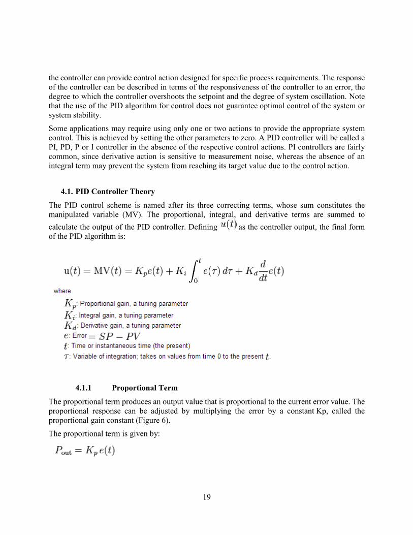
4.1. PID Controller Theory
The PID control scheme is named after its three correcting terms, whose sum constitutes the manipulated variable (MV). The proportional, integral, and derivative terms are summed to
calculate the output of the PID controller. Defining as the controller output, the final form of the PID algorithm is:
4.1.1 Proportional Term
The proportional term produces an output value that is proportional to the current error value. The proportional response can be adjusted by multiplying the error by a constant Kp, called the proportional gain constant (Figure 6).
The proportional term is given by:

20
Fig. 6. Proportional Control
A high proportional gain results in a large change in the output for a given change in the error. If the proportional gain is too high, the system can become unstable . In contrast, a small gain results in a small output response to a large input error, and a less responsive or less sensitive controller. If the proportional gain is too low, the control action may be too small when responding to system disturbances. Tuning theory and industrial practice indicate that the proportional term should contribute the bulk of the output change.
4.1.2 Integral Term
The contribution from the integral term is proportional to both the magnitude of the error and the duration of the error. The integral in a PID controller is the sum of the instantaneous error over time and gives the accumulated offset that should have been corrected previously. The
accumulated error is then multiplied by the integral gain ( ) and added to the controller output
(Figure 7).
The integral term is given by:

21
Fig. 7.Proportional -Integral Control
The integral term accelerates the movement of the process towards setpoint and eliminates the residual steady-state error that occurs with a pure proportional controller. However, since the integral term responds to accumulated errors from the past, it can cause the present value to overshoot the setpoint value.
4.1.3 Derival Term
The derivative of the process error is calculated by determining the slope of the error over time
and multiplying this rate of change by the derivative gain . The magnitude of the contribution
of the derivative term to the overall control action is termed the derivative gain, .
The derivative term is given by:
The derivative term slows the rate of change of the controller output. Derivative control is used to reduce the magnitude of the overshoot produced by the integral component and improve the combined controller-process stability. However, the derivative term slows thetransient response of the controller. Also, differentiation of a signal amplifies noise and thus this term in the controller is highly sensitive to noise in the error term, and can cause a process to become unstable if the noise and the derivative gain are sufficiently large. Hence an approximation to a differentiator with a limited bandwidth is more commonly used. Such a circuit is known as a phase-lead compensator.

22
Fig. 8. Proportional-Integral-Derivative Control
4.2 Loop Tuning
Tuning a control loop is the adjustment of its control parameters (proportional band/gain, integral gain/reset, derivative gain/rate) to the optimum values for the desired control response. Stability (bounded oscillation) is a basic requirement, but beyond that, different systems have different behavior, different applications have different requirements, and requirements may conflict with one another. PID tuning is a difficult problem, even though there are only three parameters and in principle is simple to describe, because it must satisfy complex criteria within the limitations of PID control. There are accordingly various methods for loop tuning, and more sophisticated techniques are the subject of patents; this section describes some traditional manual methods for loop tuning. Designing and tuning a PID controller appears to be conceptually intuitive, but can be hard in practice, if multiple (and often conflicting) objectives such as short transient and high stability are to be achieved. Usually, initial designs need to be adjusted repeatedly through computer simulations until the closed-loop system performs or compromises as desired. Some processes have a degree of non-linearity and so parameters that work well at full-load conditions don't work when the process is starting up from no-load; this can be corrected by gain scheduling (using different parameters in different operating regions). PID controllers often provide acceptable control using default tunings, but performance can generally be improved by careful tuning, and performance may be unacceptable with poor tuning.

23
4.3 PID Controller Implementation
In order to realize the implementation of the controller described before on the microcontroller we need to discretize it mathematical model (Figure 9).
a)
b) Figure 9.- a) Mathematical model of the PID controller in continues time, b) Mathematical
model of the PID controller in discrete time.

24
In discrete time the error signal e(t) becomes e(T) where T represent the period of the sample rate. There are many way to discretize a mathematical model, in order to reduce the development time of the project a reference model of a Discrete PID controller is used. Figure 10 shows the details of the adopted model.
Figure 10.- Discrete PID reference model. Where e(T) is the discrete error signal, Kp is the proportional gain, KI is the integrative gain and Kd is the derivative gain value. the signal y(T) is given by the next expression:
�(�) = (�� + �� + ��)�(�) − (�� + 2��)�(� − 1) + (��)�(� − 2) + �(� − 1) Where: e(T)= set point – process variable (discrete time) The factor e(T-1) is the value of the error signal delayed 1 sample, and e(T-2) is delayed twice. Now we need be focused on implement a function to perform the calculation of y(T) on the microcontroller.
4.4 Controller Physical Implementation
The Figure 11 describes the physical implementation of the Discrete PID controller using the microcontroller to calculate the value of y(T) and converting this value to a PWM signal.
Microcontroller
ADC
Boost
Converter
Input
PWM Divisor of
Voltage
PIDOutput
PWMSetpoint
Figure 11.- block diagram of physical implementation for the Discrete controller.
PID e(T) Kp Ki Kd
y(T)

25
4.5 DC-DC Converter Transfer Function
Other important thing for the discrete controller implementation is to determine the Transfer Function (TF) of the DC-DC converter before applying the PID discrete controller. Determine the TF of any system is a very hard task using analytical methods, for these reason we used the IDENT Matlab toolbox in order to determine the TF of the DC-DC converter. This tool box uses a neural network system to determine the TF of any system under analysis, the procedure is simple: this toolbox only need two data vector to realize the calculation of the TF, the firs data vector must be a series of input values for the system, and by the other hand the second data vector must be the correspond output value for each input data. If we can obtain a lot of input and output values we can achieve a better approximation of the TF for the system under analysis. The Table 1 contains a series of 24 values for the input & output data vector.
Pos Input Voltage Output Voltage
1 0 6.47V
2 560mV 56V
3 540mV 51.7V
4 680mV 56V
5 650mV 27.8V
6 790mV 34.4V
7 796mV 57.0V
8 1.08 45.0V
9 1.22 40.6V
10 1.51 37.4V
11 1.66 36.2V
12 1.8 36.1V
13 1.95 33.5V
14 2.14 31.9V
15 2.33 30.7V
16 2.52 29.3V
17 2.84 26.7V
18 2.99 25.4V
19 3.14 24.0V
20 3.28 22.6V
21 3.57 20.1V
22 3.71 18.8V
23 3.85 17.6V
24 4 16.4V Table 1.- Input/Output data vectors.

26
Once having this information we can proceed to introduce this values to the IDENT tool boox. The procedure to obtain the TF of the DC-DC converter is shown in the Figure 12.
Figure 12. Procedure to determine the TF of the DC-DC converter using the IDENT toolbox of Matlab.

27
4.6 Results
The TF calculated for the tool box :
�� =3.4556
2.5562476�^2 + 9.65648� + 8.8457
4.6.1 Finding Kp, Ki and Kd
To determine the values of Kp, Ki and Kd which satisfy the desing requirements for the DC-DC converter we use Simulink to simulate the behavior of the Discrete controller, and help to determine the required values. Figure 13 show the Simulink block diagram of the Discrete PID controller used to determine the required values.
Figure 13. Simulink block diagram of the discrete PID controller
The result values of the constants are described below Kp= 5.678 Kd= 0.015478 Ki= 1.56247

28
B. DEVELOPMET AND DESIGN OF A LIN-SLAVE
1. Requirements specification document Document Change History
Date Version Changed by 15-11-12 0.1 A. Serrano 17-11-12 0.2 A. Serrano 22-11-12 0.3 A. Serrano 25-11-12 0.4 A. Serrano 30-11-12 1.0 A. Serrano
Table of Contents
1. Purpose and Scope .......................................................................................................... 29
2.-Requirement .................................................................................................................... 30
2.1 LIN PROTOCOL OVERVIEW ............................................................................................ 30 2.1.1.- LIN message freame ...................................................................................................... 31
2.2 CONVENTIONS USED ........................................................................................................ 31
2.3. REQUIREMENT STRUCTURE ........................................................................................... 32
2.4. ACRONYMS AND ABBREVIATIONS .................................................................................. 32
3. Requirement Specification ............................................................................................ 33
3.1. FUNCTIONAL REQUIREMENTS ....................................................................................... 33 3.1.1. LIN General .................................................................................................................... 33 3.1.2 LIN Interface (slave frame handler) ................................................................................. 33 3.1.2.4. Sleep/Wake-up ............................................................................................................. 35 3.1.2.5. Error and exception handling ....................................................................................... 36 3.1.3.-LIN driver ....................................................................................................................... 36
4. 3.2 Nonfunctional requirements ................................................................................. 37
3.2.1. LIN General .................................................................................................................... 37 3.2.2. LIN interface ................................................................................................................... 40 3.2.3. LIN Driver ...................................................................................................................... 41

29
1. Purpose and Scope
This document specifies the software requirements for the Data Link Layer and the Physical Layer of the LIN Protocol according with the OSI reference model (Figure 1.1) focus on the slave nodes. The software layers mentioned before will be addressed in the following Basic Software Modules: LIN LIN Interface(Linf)
Figure 1.1. OSI reference model.
.

30
2.-Requirement
2.1 LIN Protocol Overview
LIN (Local Interconnect Network) is a concept of low cost automotive networks, which complements the existing portfolio of automotive multiplex networks. LIN will be the enabling factor for the implementation of a hierarchical vehicle network in order to gain further quality enhancement and cost reduction of vehicles. The standardization will reduce the manifold of existing low-end multiplex solutions and will cut the cost of development, production, service, and logistics in vehicle electronics. The LIN bus is a sub-bus system based on a serial communications protocol. The bus is a single master / multiple slave bus that uses a single wire to transmit data. To reduce costs, components can be driven without crystal or ceramic resonators. Time synchronization permits the correct transmission and reception of data. The system is based on a UART / SCI hardware interface that is common to most microcontrollers. The bus detects defective nodes in the network. Data checksum and parity check guarantee safety and error detection.
Figure 2.1 LIN network overview.

31
2.1.1.- LIN message freame
The LIN message frame consists of a header and a response part. The header has a fixed length while the response part consists of 0 to 8 bytes of data. The inter-frame-response time is the time it takes for a slave to respond to a request (i.e. to a ID) from the master and it may vary among the nodes on the network since it depends on the hardware and software implementation in each node. At the end of the response part a checksum, which is calculated for the data part, is attached. The header is broken up into three fields: the SYNC-break, SYNC-field and the identifier- (ID) field, which are discussed in the following sub-chapters. The structure of the message frame can be seen in Figure 2.2.
Figure 2.2 LIN message frame.
2.2 Conventions used
Requirement and objective numbers appear in bold face and within angle brackets in the left margin of this document (i.e. <R-1> or <O-1>). A number by itself defines a requirement/objective that is encompassed by the single paragraph beginning to the immediate right of the number and a table which contain the description of the requirement. The details segment in each requirement contains supporting material. Such supporting material may include explanations, justifications, and methodology.

32
Requirements are statements which express capabilities that a system must possess to gain customer acceptance. Every requirement should be identified and accepted. They should be limited to a single interpretation and stated in quantifiable and measurable terms. Objectives are not requirements, but are desirables, it is recommended they be future requirements.
2.3. Requirement structure
Each chapter contains a short functional description of the Basic Software Module. Requirements of the same kind within each chapter are grouped under the following headlines: Definitions for LIN are divided in four chapters. LIN Interface (slave frame handler). LIN Driver
2.4. Acronyms and abbreviations
Acronym Description LIN-PDU LIN Protocol Data Unit is the LIN header
and the LIN response. For example: break, synch, pid, data (1-8) and checksum.
LIN –SDU LIN Service Data Unit. The data-part of the LIN response.
LIN Driver Module name Lin. Describes the Software Driver.
LIN Interface Moduel name Linlf. Describe the LIN 1.3 slave communication stack = (LIN Slave functionality).
Sleep-mode In the LIN 2.1 specification the term stand-by and sleep mode is used in similar manner. To be consequent here only sleep-mode is used.
Abbreviation Description LIN Local Interconnect Network FF First Frame CF Consecutive Frames SF Single Frames N_PDU Network Protocol Data Unit PDUR Protocol Data Unit Router N_SDU Network Service Data Unit

33
N_TA Extended Addressing Mode Connection UART Universal Asynchronous Receiver
Transmitter. It also known as SCI and ESCI.
MRF Master request Frame SRF Slave Response Frame
3. Requirement Specification
3.1. Functional Requirements
3.1.1. LIN General
None
3.1.2 LIN Interface (slave frame handler)
3.1.2.2 Slave task
DORS ID
Requirement Description
<R1> The slave task shall be capable to identify a synchronization brake. <R2> The slave task shall be capable to synchronize on the synchronization field. <R3> The slave task must be capable to snoop the ID field in each message frame send
by the master task according with the state machine described on the Figure 3.1. Figure 3.1.- LIN Frame processor state machine.

34
<R4> The slave task shall be capable to send a response when a corresponding
ID+parity FIELD sent by the master task is requesting it (Figure 3.1). <R5> After Last data is transmitted a checksum byte shall be transmitted. <R6> The slave task shall be capable to receive a response when a corresponding
ID+parity FIELD sent by the master task is requesting it (Figure 3.1). <R7> After Last data is received a checksum byte shall be validated. <R8> Slave task must do nothing when the ID+parity FIELD sent by the master task
are not appropriate (Figure 3.1). <R9> The ID+parity FIELD shall be ensured by the network configuration in order to
avoid that more than one slaves task is unintentionally responding on a transmitted identifier.
<R10> The slave task shall generate and transmit the checksum Byte. <R11> A message shall be valid only if there is no error detected until the end of frame. <R12> Slave task should perform a fall back operation upon transmission and reception
of a corrupted message <R13> The slave task shall be capable to send a wake-up signal when bus is in sleep
mode and it needs to transmit data. <R14> The slave task shall copy the data consistently to the LIN Driver before
transmission. <R15> The slave task shall copy consistently the data to the upper layers from the LIN
driver after reception.

35
3.1.2.3 Framing
DORS ID
Requirement Description
<R16> The Slave task shall only send response fields in a message frame started by the master task.
<R17> The response field shall be manifested by zero to eight DATA FIELDS and a CHECKSUM FIELD.
<R18> The DATA FIELD shall have 8N1 codification format (Figure 3.2). Figure 3.2.- 8N1 codification format.
<R19> Every DATA FIELD shall have a length of 10 bit times. <R20> The DATA FIELD transmission shall happen LSB first (Figure 3.2). <R21> The CHECKSUM FIELD shall consist in a BYTE FIELD with 8N1 codification
(see Figure 3.2). <R22> The sum for a checksum field shall be calculated by add whit carry all data bytes
of the message frame, where carry bit each addition is added to the LSB of its resulting sum.
<R23> The checksum byte must be ‘0xFF’ (the sum of modulo 256 sum over all data bytes).
<R24> The slave node shall determine an inter frame response (H & G Figure 3.3) depending of timing considerations for the master node schedule table.
Figure 3.3.-Bite sampling.
3.1.2.4. Sleep/Wake-up
<R25> The slave node shall be capable to go to sleep mode, when the value of the ID-FIELD sent by the master task is equal to ‘0x3C’ and is followed by a zero DATA FIELD(sleep mode command).
<R26> The slave node shall not represent activity after completion of the sleep mode command until a WAKE UP SIGNAL on the bus ends the sleep mode.

36
<R27> The slave node shall be capable to send a wake up signal to the bus. <R28> The slave node shall only send a wake up signal if the bus was previously in sleep
mode and a node-internal request for wake-up is pending. <R29> The wake-up signal shall be generated with the character ‘0x80’. <R30> The first field for the wake up signal shall be given by a sequence of 8 dominant
bits. <R31> The second field for the wake up signal shall be the recessive wake up delimiter
whit a duration of at least 4 bit times. <R32> A slave node shall go back to running mode if a wake up occurs during transition
to sleep-mode.
3.1.2.5. Error and exception handling
<R33> A slave node shall be capable to monitoring the bus when it slave node is sending a bit on the bus.
<R34> A BIT_ERROR shall to be detected when the bit value that is monitored is different from the bit value that is sent.
<R35> After detection of BIT_ERROR the transmission shall be aborted latest at the next byte border.
<R36> A CHECKSUM_ERROR shall to be detected if the sum of the inverted module-256 sum over all received data bytes and the checksum does not result in ‘0xFF’
<R37> A slave node in a LIN network shall to be capable to evaluate in case of a known identifier all 8 bits of the ID-FIELD in order to distinguish between a known and a corrupted identifier.
<R38> An Inconsistent-Synch-Field-Error shall to be detected if a slave detects the edges of the SYNCH FIELD outside of +- 15% from the nominal clock rate.
3.1.3.-LIN driver
3.1.3.1 Timing Requirements
DORS ID
Requirement Description
<R39> The time required for sending a frame shall be the sum of the time to send each byte plus the response space and the inter-byte spaces.

37
<R40> In a LIN MESSAGE frame shall be considered an inter-byte space, as a period between the end of the stop bit of the preceding byte and the start bit of the following byte.
<R41> Data shall to be sampled in the middle of the bit field (Figure 3.4). Figure 3.4.-Bite sampling.
<R42> Data shall to be sampled 16 times the bit rate expected (Figure 3.5).
Figure 3.5 Bit Sampling rate.
3.2 Nonfunctional requirements
3.2.1. LIN General
None DORS ID
Requirement Description
<R43> The LIN bus shall be a system based on a serial communications protocol. <R44> The LIN physical layer shall be a wired-AND bus <R45> Every node shall have a pull-up resistor <R46> LIN system configuration shall be implemented in a Single master/ multiple slave
mode (Figure 3.6). Figure 3.6 LIN system configuration.

38
<R47> The LIN network bus shall use a single wire to transmit data. <R48> A node in LIN systems shall not use any information about the system
configuration, except for the denomination of the single master node. <R49> The system shall have the capability for add new nodes to the network without
requiring hardware or software changes in other slave nodes. <R50> The system shall have the capability of simultaneously receive and act upon
messages in any number of nodes (it can be achieved thanks to the message filtering).
<R51> Information on the bus shall be sent in fixed format messages (Figure 3.7). Figure 3.7.- LIN Message frame.
<R52> Each message frame shall starts with a break signal and is followed by a synchronization field and an identifier field (Figure 3.7).
<R53> The synchronization Break shall enable the slave nodes which have lost synchronization to identify the synchronization field.
<R54> The synchronization Break shall have a minimum bit length of 13 bits. <R55> The Synchronization field shall include five falling edges (transitions from
dominant to recessive voltage) as is shown in the Figure 3.8. Figure 3.8.- Message Synchronization field

39
<R56> The LIN system shall be capable to synchronize all the nodes in the network in
order to ensure the correct transmission and reception of data, it can be achieved measuring the distance between each falling edge in the synchronization field of the message frame.
<R57> The content of the message shall be named in the identifier field (Figure 3.8). <R58> Each node shall apply a message filtering process when receive and act upon
messages. <R59> Multiple nodes shall have the capability for receive simultaneously one message
(Multicast) using the message filtering process. <R60> The identifiers shall describe the meaning of the data in the LIN message. <R61> The maximum number of identifiers shall be 64. <R62>
The identifiers number 60, 61, 62, 63, shall be considered as reserved for special communication purposes such as software upgrades or diagnostics.
<R63> The identifier field shall have 2 reserved bits for double parity protection (Figure 3.9).
Figure 3.9.- Identifier Field.
<R64> The checksum shall be performed by inverted modulo-256 technique for the Data fields, with the carry of the MSB being added to the LSB.

40
<R65> The LIN system shall be capable to comprise between zero and eight bytes of data plus three bytes of control and data security information in each frame (Figure 3.10).
Figure 3.10.- Variable size of the data field between zero and eigth bytes.
<R66> The slave node shall receive the break signal, the synchronization field and the identifier field sent by the master task.
<R67> The slave task shall send back the data field and the check field. <R68> The slave node shall have the capability to receive the data field and the check
field sends by the master node. <R69> In case a slave node has detected an inconsistency the slave controller shall save
this information. <R70> The slave controller shall be able to provide it on request to the master control
unit in form of diagnostics information if <R69> occurs. <O71> The LIN system should have a defined fault confinement process if more than
one slave responds at the same time. <R71> The LIN system shall have a low power mode (sleep mode), in order to reduce
the system’s power consumption. <R73> The LIN system shall have a dedicated command for going to sleep mode
(SLEEP command). <R74> The LIN bus shall be recessive during sleep mode. <R75> The sleep mode shall be finished if any dominant period of a minimum length on
the bus occurs. <R76> The sleep mode shall be finished by internal conditions in any bus node. <R77> In case of node-internal wake up, a procedure based on use of the WAKE UP
SIGNAL shall be used for alerting the master. <R78> On wake up the internal activity of the system shall be re-started.
3.2.2. LIN interface
DORS ID
Requirement Description
<R79> The LIN interface implementation shall be independent from underlying LIN hardware.
<R80> The LIN interface shall have an initialization procedure

41
<R81> The LIN interface shall have the data to be transmitted from the upper layers before a transmission request by the master.
3.2.3. LIN Driver
DORS ID
Requirement Description
<R82> The LIN driver for slave nodes shall to have a timer to perform the baud rate calculation.
<R83> The LIN driver shall have an initialization procedure. <R84> The LIN interface shall be able to generate an interrupt when a synchronization
brake occurs. <R85> The maximum bit rate in a LIN system must be 20 kbit/s. <R86> The minimum bit rate in a LIN system must be 1 kbit/s. <R87> The LIN system shall be able to change the baudrate in the range specified by
<R85> and < R86> depending of the application and the user needs.

42
2. Architecture and Design document Document Change History
Date Version Changed by 20-11-12 0.1 A. Serrano 28-11-12 1.0 A. Serrano
Table of Content
1. Purpose and Scope ............................................................................................................ 43
2.-LIN General ...................................................................................................................... 43
2.1 LIN PROTOCOL OVERVIEW ....................................................................................... 43 2.2.- LIN DESCRIPTION FILE ........................................................................................... 45
3. Software Architecture ...................................................................................................... 46
3.1. LIN SW PROTOCOL HANDLING SERVICES (SLAVE NODES) ...................................... 47
4 Module design .................................................................................................................... 48
4.1 BREAK/SYNC FIELD DETECTOR .................................................................................. 48 4.2 FRAME PROCESSOR STATE MACHINE ......................................................................... 49 4.3 FLOWCHART OF THE LIN COMMUNICATION .............................................................. 51

43
1. Purpose and Scope
This document specifies the software architecture and the design for the next basic software modules: LIN Interface (Slave Frame Handler) LIN Driver The basic software modules mentioned before are focused on the slave nodes. The Transport Protocol Layer and the Application Layer are not addressed in this document.
2.-LIN General
2.1 LIN Protocol Overview
LIN Protocol supports bi-directional communication on a single wire, while using inexpensive microcontrollers driven by RC oscillators, to avoid the cost of crystals or ceramic resonators. Instead of paying the price for accurate hardware, it pays the price in time and software. The protocol includes an auto baud step on every message. Transfer rates of up to 20Kbaud are supported, along with a low power SLEEP mode, where the bus is shut down to prevent draining the battery, but the bus can be powered up by any node on the bus. Figure 2.1 shows a typical LIN Protocol configuration. The bus uses a single wire pulled high through a resistor with open collector drivers. A Dominant state is signaled by a ground level on the bus and occurs when any node pulls the bus low. A Recessive state is when the bus is at VBAT (9 - 18V) and requires that all nodes let the bus float. In the idle state, the bus floats high, pulled up through the resistor. The bus operates between 9V and 18V, but parts must survive 40V on the bus. Typically, the microcontroller is isolated from the bus levels by a line driver/receiver. This allows the microcontrollers to operate at 5V levels, while the bus operates at higher levels. The bus is terminated to VBAT at each node. The Master is terminated through a 1KW resistor, while the Slaves are terminated through a 20-47KW resistor. Maximum bus length is designed to be 40 meters. At press time (early 2000), K-Line drivers are used until true LIN drivers are available.

44
Figure 2.1 LIN Bus configuration.
Every LIN node has a physical interface which receives and transmits data to the LIN bus. The obtained data is processed by a frame handler that processes the frame. It is then sent to the application layer using the signal based interaction and transport layer. The flow of data within a LIN node is as shown in Figure 2.2.
Figure 2.2.- Layers in a LIN node.

45
2.2.- LIN Description File
As before mentioned a LIN network consist of up to 17 node (one master and 16 slaves) which communicates with each other by a number of frames, each containing several signals. To handle all these entities, The LIN-Specification states that all included nodes, schedules, frames and signals (plus other network dependent data) should be specified in a LIN Description File (LDF). This file, which is common for the complete network is the central part for the tools for LIN-networks. The analysis and simulation tools use it as a reference platform setting the rules by which the traffic should flow. The LDF is normally generated by the tools used in the earlier parts of the development process. It is a text-based file generated with a strict syntax, specified in the LIN Specification package. This file isn´t the focus of this document, but is important to know which the network architecture is specified in this file.

46
3. Software Architecture
The software architecture itself isn’t defined for a specific microcontroller, because the principal for any microcontroller is identical. In contrast to CAN or J1850, the LIN bus requires no dedicated on-chip microcontroller communication module. LIN utilizes the standard serial communication interface (USART). That is one major point for the well-balanced cost/performance ratio of this recently introduced Class A subbus. Data exchange is based on a common hardware peripheral (serial communication interface) controlled by a dedicated LIN software driver. Unlike the above mentioned in-vehicle communication protocols the high level software driver (SW Protocol handler) handles the basic communication layers and takes care of message transfers, message filtering, and error detection (Figure 3.1).
Figure 3.1 High level software driver architecture.
The low level LIN software driver entirely encapsulates the hardware modules and exclusively handles the on-chip peripherals of the microcontroller, which support serial communication.

47
Configurable software building blocks handle the LIN protocol. LIN message frame handling is done autonomously by the LIN high level software driver. Operations on LIN are at disposal of the user and are initiated by API-function calls (not discussed in this document). A LIN network based on microcontrollers can be easily realized by using the high level driver.
3.1. LIN SW Protocol Handling Services (slave nodes)
The LIN driver for slave nodes provides several API-functions for LIN bus handling. The main services of the LIN software driver are: • Message transmission • Message reception • Message filtering • Receiving "go to sleepmode" command • Sending "wake up" command • Bus timeout detection • Data length extraction • Checksum calculation

48
4 Module design
According with the requirements specification the slave node shall transmits the response when it is a publisher and receives the response when it is a subscriber. In order to obtain a design the software modules to perform the slave task according with the requirements specification, the slave task will be modeled using two state machines.
4.1 Break/sync field detector
The break / sync field detector is used in detecting the break field and synchronizing with the data rate of the LIN bus so that it can receive the rest of the data bytes of the frame, properly (Figure 4.1).
Figure 4.1.- Break/ Synch detector State machine

49
4.2 Frame processor state machine
On receiving the PID, the slave task validates the frame identifier bits with the parity and upon confirming the correctness of the frame identifier bits, it deduces one of the following three cases as listed: Case 1: Receive data
Receive data from the LIN bus. The number of bytes of data per frame identifier is
decided during node configuration.
Calculate the checksum on each byte of received data using the algorithm stated earlier.
Receive the checksum from the LIN bus.
Cross-check the received checksum with the calculated one.
If both of them match a success is reported, else an error is reported.

50
Case 2: Transmit data Transmit data to the LIN bus, again the number of data bytes per frame identifier is
decided during the node configuration.
Calculate checksum for each data byte using the algorithm stated earlier.
Transmit the checksum.
Case 3: Do nothing In case the frame identifier received has not been allocated to the slave, in such a case the
slave neither receives nor does it transmit and reverts back to idle state.
In case of a successful reception or transmission of data, a success is reported, and the slave reverts back to the idle state. In case of an error during either transmission or reception, an error is reported, and the slave reverts back to the idle state. In case of a framing error or an unknown error of PID, the slave quits and reverts back to the idle state. The set of events described above are depicted in the frame processor state machine as shown in the Figure 4.2.
Figure 4.2.- Design of the Frame processor state.

51
4.3 Flowchart of the LIN communication

52
The Figure 4.3 describes the flowchart of the two state machines describer before.
Interrupt Handler
Interrupt from fallingEdge in sync-field
First edge detected
Framing error received Last Edge Detected
Sync break already received
Sync field already received
ID field already received
Received data
Last byte sent
Last Data byte received
Checksum received
ID means send
ID means received
Check if data = 0x55
Start sync-timer
Wait for next falling edge
Stop timer and Calculate baudrate
Sync break already received
Detect sync breakERROR, reste state flagsERROR, reset state flags
Wait for ID-field
ERROR, reset state flags
Check if ID means send or receive or nothing
Send data byte
Calculate and send checksum
Receive data byte
Calculate checksum
Compare checksums for validity of data
Wait for next sync break
Wait for incoming data
Transmit one byte
Yes
Yes YesYes
Yes
Yes
Yes
Yes
Yes
Yes
Yes
Yes
Yes
Yes
No No
NoNo
No
No
No
No
No
Yes
No
No
No
No
No
No
Flow chart of the LIN-communication

53
3. Test documet Document Change History
Date Version Changed by 30-11-12 0.1 A. Serrano 30-12-12 1.0 A. Serrano

54
Table of Content
1. Purpose and Scope .......................................................................................................... 54
2.-Test description ............................................................................................................... 54
3. Test cases.......................................................................................................................... 55
3.1LIN INTERFACE ........................................................................................................ 55 3.1.1 LIN Slave task .........................................................................................................55 3.1.2 LIN Slave Framing..................................................................................................63 3.1.3 Sleep/ wake up ........................................................................................................66 3.1.3. Error and exception handling .................................................................................68
1. Purpose and Scope
The porpoise of this document is to describe a test procedures for the LIN protocol implementation for the slave nodes (SYSTEM/INTEGRATION Testing) this test procedure must be performed by the test manager and development team leader with assistance from the individual developers as required.
2.-Test description
Test cases described in this document are grouped to be executed following the preconditions each test case indicates respectively. Each test case contains a number of steps that must be executed under the series which have been defined.

55
3. Test cases
3.1LIN Interface
3.1.1 LIN Slave task
TC-LIN01
Type Black Box
Requirement Reference <R1>,<R82>,<R83>,<R84> <R85>,<R86>,<R87>.
Pre-condition
1.- The debugger tool is running in the PC. 2.-The user has connected the develop board to the PC via USB. 3.- The microcontroller has been flashed with the software module release. LIN_protocol_implementation(slave)v1.0. 4. The slave node is connected to a LIN network with at least a master node. 5.- The master node is ready to run an application with a pre-configured LIN description file. 6.- The watch window of the debugger tool is displayed in the computer screen, and the global variables “p”, “Five_Five”,”ID_Found”, “flagE1” & “flag4F” “check_sumres” are monitored.
Post-condition
TC-LIN02
Purpose Detect the Synchronization Break Test Description
Step Action Expected response current response Comments
1
Place a break point in the Line 151 of the LIN_comm_protocol.c file
2 Run the application
3 Send a Synch Break signal
The debugger reaches the breakpoint
The debugger reaches the breakpoint
The slave task state machine is waiting for the

56
synchronization field
TC-LIN02
Type Black Box
Requirement Reference <R2>,<R38>, <R39>,<R40> <R41>
Pre-condition TC-LIN01
Post-condition None
Purpose Synchronize the slave node with the master.
Test Description
Step Action Expected response current response Comments
1
Place a break point in the Line 162 of the LIN_comm_protocol.c file
2 Run the application
3 Send a Synch Field signal
The debugger reaches the breakpoint
The debugger reaches the breakpoint
The slave task state machine is waiting for the ID FIeld
4
The watch window display: Five_Five = 0x55 ID_found = 1 p = 1 flag4F=0 flagE1=0 check_sumres=0
The watch window display: Five_Five = 0x55 ID_found = 1 p = 1 flag4F=0 flagE1=0 check_sumres=0
TC-LIN03
Type Black Box
Requirement Reference <R3> , <R4>
Pre-condition TC-LIN02
Post-condition None
Purpose Check a transmission ID Field

57
Test Description
Step Action Expected response current
response Comments
1
Place a break point in the Line 186 of the LIN_comm_protocol.c file
2 Run the application
3 Send an ID Field 0X4F The debugger reaches the breakpoint
The debugger reaches the breakpoint
The slave task state machine identified an ID for transmission
4
The watch window display: Five_Five = 0x55 ID_found = 1 p = 2 flag4F=1 flagE1=0 check_sumres=0
The watch window display: Five_Five = 0x55 ID_found = 1 p = 2 flag4F=1 flagE1=0 check_sumres=0
TC-LIN04
Type Black Box
Requirement Reference <R5>,<R10>,<R11> <R23>,<R22>
Pre-condition TC-LIN03
Post-condition None
Purpose Calculate a CheckSum to be transmitted

58
Test Description
Step Action Expected response current response Comments
1
Place a break point in the Line 388 of the LIN_comm_protocol.c file
2 Run the application
3 The debugger reaches the breakpoint
The debugger reaches the breakpoint
The slave task state machine calculates the CheckSum Field to be transmited.
4
The watch window display: Five_Five = 0x55 ID_found = 1 p = 2 flag4F=1 flagE1=0 check_sumres=0xFF
The watch window display: Five_Five = 0x55 ID_found = 1 p = 2 flag4F=1 flagE1=0
check_sumres=0xFF
TC-LIN05
Type Black Box
Requirement Reference <R3>, <R8>
Pre-condition TC-LIN02
Post-condition None
Purpose Check an incorrect ID Field Test Description
Step Action Expected response current response Comments

59
1
Place a break point in the Line 186 of the LIN_comm_protocol.c file
2 Run the application
3 Send an ID Field 0X00 The debugger reaches the breakpoint
The debugger reaches the breakpoint
The slave task state machine
4
The watch window display: Five_Five = 0x55 ID_found = 1 p = 0 flag4F=0 flagE1=0 check_sumres=0
The watch window display: Five_Five = 0x55 ID_found = 1 p = 0 flag4F=0 flagE1=0 check_sumres=0
TC-LIN06
Type Black Box
Requirement Reference <R3>,<R6>
Pre-condition TC-LIN02
Post-condition TC-LIN07
Purpose Check a Reception ID Field Test Description
Step Action Expected response current
response Comments
1
Place a break point in the Line 186 of the LIN_comm_protocol.c file

60
2 Run the application
3 Send an ID Field 0XE1 The debugger reaches the breakpoint
The debugger reaches the breakpoint
The slave task state machine
4
The watch window display: Five_Five = 0x55 ID_found = 1 p = 2 flag4F=0 flagE1=1 check_sumres=0
The watch window display: Five_Five = 0x55 ID_found = 1 p = 2 flag4F=0 flagE1=1 check_sumres=0
TC-LIN07
Type Black Box
Requirement Reference <R7>,<R22>,<R23>
Pre-condition TC-LIN06
Post-condition None
Purpose Validate a received CheckSum
Test Description
Step Action Expected response current response Comments
1
Place a break point in the Line 415 of the LIN_comm_protocol.c file
2 Run the application
3 The debugger reach the break point
The debugger reach the break point
The slave task state machine

61
validates the received checksum
4
The watch window display: Five_Five = 0x55 ID_found = 1 p = 2 flag4F=0 flagE1=1 check_sumres=0xFF
The watch window display: Five_Five = 0x55 ID_found = 1 p = 2 flag4F=0 flagE1=1 check_sumres=0xFF
TC-LIN08
Type Black Box
Requirement Reference <R14>
Pre-condition
TC-LIN03 The global variable u8SCI0_TxData is added to the watch window
Post-condition None
Purpose Copy consistent data from the LIN interface to the LIN driver
Test Description
Step Action Expected response current response Comments
1 Place a break point in the Line 389 of the LIN_comm_protocol.c file

62
2 Set the variable ai8AnalogSignalName0[0] = 0xA1
3 Run the application
4 The debugger reaches the breakpoint
The debugger reaches the breakpoint
5
The watch window display: Five_Five = 0x55 ID_found = 1 p = 2 flag4F=0 flagE1=1 check_sumres=0xFF u8SCI0_TxData= 0xA1
The watch window display: Five_Five = 0x55 ID_found = 1 p = 2 flag4F=0 flagE1=1 check_sumres=0xFF u8SCI0_TxData= 0xA1
TC-LIN09
Type Black Box
Requirement Reference <R15>
Pre-condition
TC-LIN07 The global variable u8SCI0_RxData is added to the watch window
Post-condition None
Purpose Copy consistent data from the LIN driver to the LIN interface
Test Description
Step Action Expected response current response Comments
1
Place a break point in the Line 415 of the LIN_comm_protocol.c file

63
2 Run the application
3 Send from the master a DATA Byte of 0xAF
4 The debugger reaches the breakpoint
The debugger reaches the breakpoint
5
The watch window display: Five_Five = 0x55 ID_found = 1 p = 2 flag4F=0 flagE1=1 check_sumres=0xFF u8SCI0_RxData= 0xAF
The watch window display: Five_Five = 0x55 ID_found = 1 p = 2 flag4F=0 flagE1=1 check_sumres=0xFF u8SCI0_RxData= 0xAF
3.1.2 LIN Slave Framing
TC-LIN10
Type Black Box
Requirement Reference
<R16> <R17> <R33> <R32>
Pre-condition TC-LIN03
Post-condition None
Purpose Validate the RESPONCE FIELD
Test Description Step
Action Expected response
current response Comments
1 Place a break point in the Line 395 of
the LIN_comm_protocol.c file

64
2
Change the line 34 of the LIN_comm_protocol.c file by the next line: INT8 ai8AnalogSignalName0[3]={0xA1,0xB2,0xC3};
3 Initialize and connect the LIN analyzer tool to the LIN channel 0
4 Run the application The debugger reaches the break point
The debugger reaches the break point
5
The analyzer decodes the sent data bytes and displays the values 0xA1 0xB2 0xC3 0xFF (Checksum)
The analyzer decodes the sent data bytes and displays the values 0xA1 0xB2 0xC3 0xFF
TC-LIN11
Type Black Box
Requirement Reference <R16> <R17>
Pre-condition TC-LIN03
Post-condition None
Purpose Validate the RESPONCE FIELD
Test Description Step
Action Expected response
current response Comments
1 Place a break point in the Line 395 of
the LIN_comm_protocol.c file
2
Change the line 34 of the LIN_comm_protocol.c file by the next line: INT8 ai8AnalogSignalName0[8]={0xD4,0xE5, 0xF6,0xF1,0xAF,0xDE,0xEE,0x00};

65
3 Initialize and connect the LIN analyzer tool to the LIN channel 0
4 Run the application The debugger reaches the break point
The debugger reaches the break point
5
The analyzer decodes the sent data bytes and displays the values 0xD4 0xE5 0xF6 0xF1 0xAF 0xDE 0xEE 0x00 0xFF (Checksum)
The analyzer decodes the sent data bytes and displays the values 0xD4 0xE5 0xF6 0xF1 0xAF 0xDE 0xEE 0x00 0xFF
TC-LIN12
Type Black Box
Requirement Reference <R18> , <R19>,<R18>
Pre-condition TC-LIN11
Post-condition None
Purpose Validate the 8N1 codification of the Data Fields
Test Description Step
Action Expected response
current response Comments
1 Run the application
2 The analyzer tool displays the wave form of the Response Frame
The data bytes have a 8N1 codification format
The data bytes have a 8N1 codification format

66
3 The first bit transmitted is the LSB
The first bit transmitted is the LSB
TC-LIN13
Type Black Box
Requirement Reference <R21>
Pre-condition TC-LIN11
Post-condition None
Purpose Validate the 8N1 codification of the CheckSum Field
Test Description Step
Action Expected response
current response Comments
1 Run the application
2 The analyzer tool displays the wave form of the Response Frame
The CheckSum Field have a 8N1 codification format
The data bytes have a 8N1 codification format
3.1.3 Sleep/ wake up
TC-LIN14
Type Black Box
Requirement Reference <R24> , <R25>
Pre-condition TC-LIN01
Post-condition None
Purpose Execute go to sleep command
Test Description Step
Action Expected response
current response Comments
1 Place a break point in the Line 500 of the LIN_comm_protocol.c file

67
2 Send a sleep command from the master node
The slave node is in sleep mode
The slave node is in sleep mode
2.1.1
TC-LIN15
Type Black Box
Requirement Reference <R26>, <R27>,<R31>
Pre-condition
TC-LIN14 A new watch(2) window is open and WakeupFlag variable is watched
Post-condition None
Purpose Execute a wake up procedure
Test Description Step
Action Expected response
current response Comments
1 Place a break point in the Line 600 of the LIN_comm_protocol.c file
2 Set the value of the WakeupFlag = 1 in the watch(2) window
The watch(2) window display: WakeupFlag = 1
The watch(2) window display: WakeupFlag = 1
3 The debugger reaches the break point
The debugger reaches the break point
4 The slave node is in sunning mode
The slave node is in sunning mode
TC-LIN16
Type Black Box

68
Requirement Reference <R28>, <R29>,<R30>
Pre-condition TC-LIN14
Post-condition None
Purpose Validate the wake up signal
Test Description Step
Action Expected response
current response Comments
1 Place a break point in the Line 635 of the LIN_comm_protocol.c file
2 Initialize and connect the LIN analyzer tool to the LIN channel 0
3 Execute TC-LIN15 skipping step 1
The watch(2) window display: WakeupFlag = 1
The watch(2) window display: WakeupFlag = 1
4
The LIN analyzer tool decode the wake up signal as 0x80
The LIN analyzer tool decode the wake up signal as 0x80
5 The debugger reaches the break point
The debugger reaches the break point
6 The slave node is in sunning mode
The slave node is in sunning mode
3.1.3. Error and exception handling

69
TC-LIN17
Type Black Box
Requirement Reference <R36>
Pre-condition TC-LIN06
Post-condition None
Purpose Validate an ID field to avoid ID errors
Test Description Step
Action Expected response
current response Comments
1 Place a break point in the Line 295 of the LIN_comm_protocol.c file
2 Run the application The debugger reaches the break point
The debugger reaches the break point
3
The watch window display: Five_Five = 0x55 ID_found = 1 p = 2 flag4F=0 flagE1=1
The watch window display: Five_Five = 0x55 ID_found = 1 p = 2 flag4F=0 flagE1=1
TC-LIN18
Type Black Box
Requirement Reference <R36>
Pre-condition TC-LIN11
Post-condition None
Purpose Validate an ID field to avoid ID errors
Test Description Step
Action Expected response
current response Comments
1 Place a break point in the Line 295 of the LIN_comm_protocol.c file
2 Run the application The debugger reaches the break point
The debugger reaches the break point

70
4. Test plan
Table of Content
1. TEST PLAN IDENTIFIER ........................................................................................ 71
2. REFERENCES ............................................................................................................ 71
3. INTRODUCTION ....................................................................................................... 71
4. TEST ITEMS ............................................................................................................... 71
5. SOFTWARE RISK ISSUES ....................................................................................... 71
6. FEATURES TO BE TESTED .................................................................................... 71
7. FEATURES NOT TO BE TESTED .......................................................................... 72
8. APPROACH................................................................................................................. 72
8.1 TESTING LEVELS .................................................................................................... 72 8.2 CONFIGURATION MANAGEMENT ........................................................................... 72 8.3 TEST TOOLS ........................................................................................................... 72 8.4 MEASURES AN METRICS......................................................................................... 72
9. ITEM PASS/FAIL CRITERIA .................................................................................. 73
10. SUSPENSION CRITERIA AND RESUMPTION REQIREMENTS..................... 73
11. TEST DELIVERABLES ............................................................................................. 73
12. REMAINING TEST TASK ........................................................................................ 73
13. ENVIROMENTAL NEEDS........................................................................................ 73
14. STAFFING AND TRAINING NEEDS ...................................................................... 73
15. RESPONSABILITIES................................................................................................. 73
16. SCHEDULE ................................................................................................................. 73
17. PLANNING RISK AND CONTINGENCIES ........................................................... 74
18. APPROVALS ............................................................................................................... 74

71
1. TEST PLAN IDENTIFIER SDC-MTP00.1
2. REFERENCES
LIN Protocol Specification V 1.3
3. INTRODUCTION
This is the Master Test Plan for the LIN protocol for the slave nodes project. This plan will address only those items and elements that are related to the LIN Protocol for the slave nodes project, both directly and indirectly affected elements will be addressed. The primary of this plan is to ensure that the LIN slave nodes can establish communication in a LIN network. The project will have only the System/Integration level of testing. The details for this level are addressed in the approach section and will be further defined in the level specific plans. The estimated time line for this project is one (1) week, as such, any delays in the development process could have significant effects on the test plan.
4. TEST ITEMS
The following is a list, by version and release, of the items to be tested: No. Item Version 1 LIN_Interface 1.0 2 LIN_Driver 1.0
5. SOFTWARE RISK ISSUES
The Short Delivery time is the only risk identified.
6. FEATURES TO BE TESTED
The following is a list of the areas to be focused on during testing of the LIN protocol. No. Item 1 The process to generate a LIN Response Frame. 2 The process to receive a LIN Message Frame 3 The process to detect a synchronization break sends by the master
node. 4 The proper synchronization process

72
7. FEATURES NOT TO BE TESTED
The following is a list of the areas that will not be specifically addressed. All testing in these areas will be indirect as a result of other testing efforts. No. Item 1 The User Application 2 The Transport Protocol
8. APPROACH
8.1 Testing levels
The testing for the LIN protocol project will consist only in System/Integration test level. It is hoped that there will be at least one full time independent test person for system/integration testing. Most testing will be done by the test manager with the development teams participation.
8.2 Configuration management
SYSTEM/INTEGRATION Testing will be performed by the test manager and development team leader with assistance from the individual developers as required. No specific test tools are available for this project. Programs will enter into System/Integration test after all critical defects have been corrected. A program may have up to two Major defects as long as they do not impede testing of the program.
8.3 Test tools
The tools to be used to test the items will be the corresponding debugger for the used development platform and a logic analyzer for the LIN protocol.
8.4 Measures an metrics
The following information will be collected by the test team during the system/integration testing process. This information will be provided to the development team in order to revert all the defects detected. 1. Defects by module and severity. 2. Defect Origin (Requirement, Design, Code) 3. Time spent on defect investigation by defect, for Critical & Major only. All Minor defects can be totaled together. 4. Number of times a program submitted to test team as ready for test. 5. Defects located at higher levels that should have been caught at lower levels of testing.

73
9. ITEM PASS/FAIL CRITERIA
The test process will be completed once the slave node can execute with property the synchronization process, receive an ID field and when the ID correspond to this slave node generate a LIN response frame or receive it.
10. SUSPENSION CRITERIA AND RESUMPTION REQIREMENTS
There aren’t suspension criteria for this test plan.
11. TEST DELIVERABLES
System/Integration test plan Defect/Incident reports and summaries Test logs and turnover reports
12. REMAINING TEST TASK
All the tasks must be done by the test manager.
13. ENVIROMENTAL NEEDS
In order to execute this master test plan will require the installation of the CodeWarrior V10.1 debugging tool. Also will be necessary to have a LIN network that at least has the master node. The master node must have the ability to establish a communication agree with LIN protocol version 1.3
14. STAFFING AND TRAINING NEEDS
Advanced Knowledge in the debugger tool.
15. RESPONSABILITIES
The development team leader will be responsible for the verification and acceptance of all unit test plans and documentation. The project manager/test manager is responsible for all test plans and documentation.
16. SCHEDULE
Stage/hours 10 12 14 16 18 20 Integration test

74
17. PLANNING RISK AND CONTINGENCIES
In order to achieve with the deadline for execute this test plan the Development manager will brings help to the Test manager if some delays occur during the test process.
18. APPROVALS
Sponsor- Hector Rivas Test manager- TDB Development manager- Abdiel Serrano

75
C. EMBEDDED BODY CONTROLLER MODULE
Table of Content
3. CHAPTER ONE - OVERVIEW ................................................................................ 77
4. CHAPTER TWO – ARCHITECTURE .................................................................... 79
4.1. SOFTWARE ARCHITECTURE ........................................................................................ 79 4.1.1 Software layer description ........................................................................................... 79
System Services (Operating System): ............................................................................................................................. 79 4.2. HARDWARE ARCHITECTURE ....................................................................................... 81
5. CHAPTER THREE – DESIGN .................................................................................. 83
5.1. SOFTWARE DESIGN ...................................................................................................... 83 5.1.1 Scheduler ...................................................................................................................... 83 5.1.2 MCU Abstraction Layer ............................................................................................... 88
Communication drivers ................................................................................................................................................... 88 CAN driver. ............................................................................................................................................................... 88
Input/output drivers ......................................................................................................................................................... 91 PWM driver. .............................................................................................................................................................. 91 ADC driver. ............................................................................................................................................................... 93 GPIO driver. .............................................................................................................................................................. 95
System Drivers ................................................................................................................................................................ 98 PIT Driver. ................................................................................................................................................................. 98 Watchdog driver. ....................................................................................................................................................... 99 Background (Memory Checksum). ............................................................................................................................ 99 5.1.3 ECU abstraction layer ............................................................................................... 101
Communication Hardware Abstraction ......................................................................................................................... 102 CAN Handler. .......................................................................................................................................................... 102
Input/output Hardware Abstraction ............................................................................................................................... 103 ADC Handler. .......................................................................................................................................................... 103
Application.................................................................................................................................................................... 107 Low power management. ......................................................................................................................................... 107
5.2. HARDWARE DESIGN ................................................................................................... 108 5.2.1 Bill of materials (BOM) ............................................................................................. 108 5.2.2 Sensors ....................................................................................................................... 108
Temperature .................................................................................................................................................................. 109 Performances Voltage/Temperature: ....................................................................................................................... 109
Humidity ....................................................................................................................................................................... 110 Speed............................................................................................................................................................................. 111 Battery Voltage ............................................................................................................................................................. 112 Proximity ...................................................................................................................................................................... 113 Key status ...................................................................................................................................................................... 114 Brake pedal ................................................................................................................................................................... 115
5.2.3 Actuators .................................................................................................................... 117 Lights ............................................................................................................................................................................ 117 Extreme switch ............................................................................................................................................................. 118
6. CONCLUSIONS ........................................................................................................ 119
7. Bibliography ............................................................................................................... 120
8. APPENDIX A: ............................................................................................................ 121

76
8.1. KEY WORDS ............................................................................................................... 121
8.2. IDENTIFIER ................................................................................................................. 121
8.3. REQUIREMENTS ................................................................................................... 122
9. APPENDIX B: SYSTEM TEST BENCH ................................................................ 129
9.1. PURPOSE AND SCOPE .......................................................................................... 129
9.2. TEST DESCRIPTION ..................................................................................................... 129
9.3. TEST CASES ............................................................................................................ 129
9.4. BMC HARDWARE/SOFTWARE INTERFACES .............................................................. 129 9.4.1 129 9.4.2 Real Time Operative System ...................................................................................... 130 9.4.3 On Board Device ........................................................................................................ 130
Analog to Digital Converter (ADC) .............................................................................................................................. 131 Pulse Width Modulator (PWM) .................................................................................................................................... 133
9.4.4 Communication .......................................................................................................... 136 Controller Area Network (CAN)................................................................................................................................... 136
9.4.5 Digital Input Output (GPIO) ...................................................................................... 139 9.4.6 Application ................................................................................................................. 140
Low Voltage Detection ................................................................................................................................................. 140 9.5. BMC HARDWARE INTERFACES................................................................................. 141
9.5.1 Sensors ....................................................................................................................... 141 Environment Humidity ................................................................................................................................................. 141 Speed............................................................................................................................................................................. 142 Fuel Level ..................................................................................................................................................................... 143 Proximity ...................................................................................................................................................................... 145 Temperature .................................................................................................................................................................. 146
9.6. ACTUATORS................................................................................................................ 147 Power light controller.................................................................................................................................................... 147

77
3. CHAPTER ONE - OVERVIEW
In automotive electronics, body control module (BCM) is a generic term for an electronic control unit responsible for monitoring and controlling various electronic accessories in a vehicle's body. Typically in a car the BCM controls the power windows, power mirrors, air conditioning, immobilizer system, central locking, etc. “The Load Control can either be directly from BCM or via CAN/LIN communication with remote ECUS. The central body controller often incorporates RFID functions like remote keyless entry and immobilizer (Texas Instruments, 2013)”.
Figure 1. BCM system.
Optimization and advanced developments in terms of comfort, safety and variety are already presenting a great challenge to the vehicle electric system. The Body Control Module (BCM) is the core component for the realization of a broad range of functions. This central control unit can combine classic power distribution and the safeguarding of relay and fuse boxes with the advantages of intelligent, micro-controller controlled systems. In addition, BCMs play a deciding role in cost efficiency as they allow for the amount wiring within the vehicle to be significantly reduced by providing interfaces for bus systems. Depending on the architecture approach different variants of central control units can be created from numerous combination possibilities. From more universal entry-level BCMs to highly integrated variants see Figure 1. The Figure 2 is a block diagram that describes the interaction with the external world, for instance: measure the temperature inside the car and regular it with the air conditioning, this is the reason whereby the BCM take over the sensors and actuators.

78
Figure 2: BCM project.
The BCM project was developed in based to the requirements given for the costumers, and checked every one by the developers, the requirements are in Requirements section, noteworthy that the scheduler (part of a RTOS) was proposed by the developers team.

79
4. CHAPTER TWO – ARCHITECTURE
This chapter describes the software and hardware architecture. To software architecture is taken as reference the model AUTOSAR (Automotive Open System Architecture), but does not comply with AUTOSAR, it just used some elements like the sorting of software layers.
4.1. Software Architecture
In order to cover the requirements specification of this implementation, software architecture was proposed, based only in the structure of software layers suggested by AUTOSAR, and it is not compliant with the AUTOSAR spec. This implementation considers using the next software layers:
Application Layer
ECU Abstraction Layer
MCU Abstraction Layer
System services layer
4.1.1 Software layer description
System Services (Operating System): This layer will contain the Scheduler, Hardware configuration and Interrupt handler. Scheduler: This module will be responsible for managing the CPU usage, some of its features are:
o configured and scaled statically
o amenable to reasoning of real-time performance
o will provides a priority-based scheduling
Interrupt Handler: It module will be in charge of manage the next system interrupts: o Periodic Timer Interrupts
o Communication Interrupts
o I/O Interrupts
Communication This layer will be responsible of handling the communication Framework, of CAN and SPI interphases, the I/O management for these interphases and, Network management.

80
Microcontroller Abstraction (MCU) Access to the hardware is routed through the Microcontroller Abstraction layer (MCAL) to avoid direct access to microcontroller registers from higher-level software. MCAL will be used as hardware specific layer that ensures a standard interface to the components of the ECU Software Layer. It will manage the microcontroller peripherals and will provide the components of the ECU with microcontroller independent values. MCAL also will implement notification mechanisms to support the distribution of commands, responses and information to different processes. This layer will include handling of:
o Digital I/O (DIO)
o Analog/Digital Converter (ADC)
o Pulse Width (De)Modulator (PWM, PWD)
o Capture Compare Unit (CCU)
o Watchdog Timer (WDT)
o Serial Peripheral Interface (SPI)
o Controller Area Network Bus (CAN)
I/O Hardware Abstraction (ECU Abstraction) The ECU Abstraction will provide a software interface to the electrical values of any specific ECU to decouple higher-level software from all underlying hardware dependencies.
Application Layer (APL): This layer will be in charge of the low power management, enabling the possibly for change the operation mode of the BCM to low consumption mode. Software architecture is implemented as shown in block diagram of the Figure 3.

81
Figure 3: Software architecture.
4.2. Hardware Architecture
This section describes how interact all stages in the hardware such as control stages, power stage, etc. The Figure 4 shown those stages, it also shown that the system work with a closed control system, a clear example is the temperature control (only in automatic mode) the control must keep the same temperature. The sensors are connected into the analog/digital input, known as GPIO. To manage actuators the BCM used as power stage an Extreme Switch board, this one has four PWM input ports, it also has a serial communication (SPI is not used) full description will be seen in hardware design section.
The BCM communicates with other systems through the CAN network. It is able to transmit and receive messages from the cluster.
Communication Drivers
SP
I D
river
CA
N D
river
I/O Drivers
AD
C D
river
GP
IO D
river
FL
AS
H
SP
I
CA
N
PW
M
AD
C
GP
IO
Communication Hardware Abstraction I/O Hardware Abstraction
Drivers for Extern PWM
ADC Handler
CAN Handler SPI Handler
Onboard Device Abstraction
System Drivers
PLL
Drive
r
Watc
hdo
g D
rive
rW
DT
Microcontroller
Operative S
System Services
Sched
ule
r
Interrupt
Application Low Power Management
PIT
Driver
PW
M D
river
PW
M
AD
C D
river
PLL
PIT

82
Figure 4: Hardware architecture.
The ECU is a kit develop board DEMO9S12XEP100 by Freescale, these are the main characteristics:
- 112-pin LQFP MC9S12XEP100 MCU
- Selectable 4 MHz Crystal and a provision for an oscillator module (socketed)
- Built-in USB to BDM interface for in-circuit debugging
- Provision for a BDM connector for external in-circuit debugging
- Header connectors with all MCU signals
- One CAN connector with transceiver
- Two LIN connector with one transceiver
- One RS-232 connector with transceiver
- Four user LEDs
- Four DIP-switches
- Potentiometer for analog input
- Light sensor
- 2 push buttons
- Reset push button

83
5. CHAPTER THREE – DESIGN
This chapter delves into the design of each block of the software and hardware architecture, it also delves into the scheduler design since it is not part of the requirements is the core part of the project.
5.1. Software Design
Taking the previous concept the last Chapter, building the architecture that was adapted to the requirements. The design exhibit an architectural structure, contain interfaces that reduces the complexity of connections between modules and external environment. Below is described the cycle life to develop the BCM project. Some of the next steps had to rethink because functionalities were added to the project.
1. Requirements: First identify the problem and classify the requirements in functional and not-
functional.
2. Analyze and build the model of problem: In this part building the first version of model, it was
based in AUTOSAR but at the end it just take AUTOSAR as reference.
3. Postulate a design solution: In this point, taking the elements and modules necessary for building
the architecture of software.
4. Validate Solution: V-Model permitted to validate the design.
5. Refine Design Solution: This step is iterative in all design.
6. Implement Solution: Programming the software design in C language using the IDE of Freescale
(Code Warrior 10.3).
5.1.1 Scheduler
The BCM project does not use a real time operative system as such, rather uses only a part of it, due to is not necessary to use a RTOS to this implementation. The real time scheduler uses a real time periodic interrupt (implemented by hardware) in order to generate the heartbeat of the operative system, this heartbeat is known as the OS tick.
The flow of interrupt service routine (ISR) of the timer interrupt is described in the Figure 5, keep in mind to setting the timer interrupt, must be configured before the PLL.

84
Figure 5: ISR of the periodic timer interrupt.
The configuration of the tasks to be executed is performed by the task tables, this tables are a set of periodic task which will be executed for the scheduler to the operation of the BCM. This implementation can have different task tables to offer flexibility for configure different modes of operation for the BCM. The modes of operation can be selected as normal mode and low voltage mode. Table 1 show how these tables are structured. A Fully cooperative scheduling algorithm is used to schedule the execution of the all task in the system.
Table 1: Task table definitions
Task Name Functions Rate [mS] Task2MS Debounce Key Status
Debounce Brake Pedal 2
Task4MS Get Battery Level Get Brake Pedal Status
4
Task8MS Set PWM Duty Cycle Send Data to Cluster Get Lights Signal Status Get Stalk Status
8
Task16MS Process Received CAN Frames 16 Task32MS Set PWM Duty Cycle
Transmit Stalk Status Transmit Lights Status Transmit Brake Pedal Status
32

85
To start the execution of the tasks, the selection of the active table must be performed. This means that after the hardware configuration, the real time scheduler needs to find the active task table, validate that the table is the correct one and store the address of the valid table for the Kernel. This procedure is represented in the flow diagram of the Figure 6.

86
(From Hardware Configuration)
Prepare first OS task table ()
Load address of the linked list of task structures
Is a valid task table address found ?
Reset OS Clocks?
Yes
Store address for OS Kernel
Is null Position?
No
point to the next table in the list
No
End
Yes
Reset OS Clock
Yes
No
This value will be used in the main Kernel
Figure 6: Flow Diagram of the preparation of the first OS task table.

87
The decision of which task will be executed will be performed by the kernel of the scheduler. The logic implementation of this module is illustrated in Figure 7.
Figure 7: OS kernel block diagram.

88
5.1.2 MCU Abstraction Layer
This layer is the lowest software layer of the basic software. It contains internal drivers, which are software modules with direct access to the microcontroller internal peripherals and memory mapped microcontroller external devices. Its task is to make higher software layers independent of microcontroller.
Communication drivers A driver contains the functionality to control and access an internal or an external device. This project contains the follow drivers, that will be describe one by one.
CAN driver.
CAN Bus is a vehicle bus standard designed to allow microcontrollers and devices to communicate with each other a vehicle without a host computer. Also it is a message-based- protocol, designed specifically for automotive. “The module is a communication controller implementing the CAN 2.0A/B protocol as defined in the Bosch specification dated September 1991” (Freescale Semiconductor, MC9S12XEP100 Reference Manual, 2012). Some characteristic are:
• Implementation of the CAN protocol — Version 2.0A/B — Standard and extended data frames — Zero to eight bytes data length — Programmable bit rate up to 1 Mbps1 — Support for remote frames
• Five receive buffers with FIFO storage scheme • Three transmit buffers with internal prioritization using a “local priority” concept • Flexible maskable identifier filter supports two full-size (32-bit) extended identifier filters, or four 16-bit filters, or eight 8-bit filters • Programmable wake-up functionality with integrated low-pass filter • Programmable loopback mode supports self-test operation • Programmable listen-only mode for monitoring of CAN bus • Programmable bus-off recovery functionality • Separate signaling and interrupt capabilities for all CAN receiver and transmitter error states (warning, error passive, bus-off) • Programmable MSCAN clock source either bus clock or oscillator clock • Internal timer for time-stamping of received and transmitted messages • Three low-power modes: sleep, power down, and MSCAN enable • Global initialization of configuration registers
The CAN bus driver allows communication between BCM and Cluster, it is able to send/receive messages, Figure 8.

89
CAN_Init
- MSCAN Initialization Mode- Initialization Mode Acknolewdge-Clock Source (XTAL)-Baud Rate(500KBps)- CAN_Acceptance_FiltersInit()-Exit Iniatilization Mode Request- Wait Normal Mode- Clear Receiver Flags- Acces Configuration Data Registers- CAN Rx Channel 0- Enable Full Receive Buffer Interrupt
CAN_Acceptance_FiltersInit()
- CANOIDAC_IDAM = 0x0116 Bit Filter
CAN_SenFrame(ID,Priority,Length,Data)
Interrupt CAN_RX
-Conditions: if EXT frame has been received CAN_RX_Buffers.ID-Extract received frame data length CAN_RX_Buffers.Length-Extract received frame data bytes-Raise Flag to signal that new data is available for current message-Clear Reception Flag
-Transmission Buffet-Index to data within the transmission buffer- Condition IF Check for TX buffer availabil ity, if all 3
TX buffers are full-Select lowest empty buffer-Backup selected buffer- Load ID to IDR registers- Load data to Data Segment Registers- Load Length Code- Load Priority- Start Transmission
CAN DRIVER
Figure 8: CAN block diagram.
void vfnCAN_init (void)
Description This function initialize and configure CAN, wait for initialization mode acknowledge
Parameter 1 Void Return Value Void Precondition Function can only be called when the all drivers are initialization.
Post condition Enabling MSCAN, configure baud rate, acceptance filters. Error Conditions None
void vfnCAN_BaudRateConfig (void)
Description Configure the baud rate of CAN. Parameter 1 Void
Return Value void Precondition Function can only be called once the CAN was initialized.
Post condition CAN CLK, Baud Rate & Pre-scaler will be enabled. Error Conditions None
UINT8 u8CAN_SendFrame(UINT32 u32ID, UINT8 u8Prio, UINT8 u8Length, UINT8 *u8TxData)
Description Transmit Data Frame Parameter 1 UINT32 u32ID (Identifier which represent the priority of message ) Parameter 2 UINT8 u8Prio (Priority based on bus arbitration) Parameter 3 UINT8 u8Length (Length section of data) Parameter 4 UINT8 *u8TxData (Data to be transmitted)

90
Return Value NO_ERR (if the frame was sent successfully, it return NO_ERR) Precondition Function can only be called once the CAN was initialized, and baud rate as
well. Post condition CAN CLK, Baud Rate & Pre-scaler will be enabled.
Error Conditions None

91
Input/output drivers It contains the drivers for Analog and Digital Signals, with this signal the BMC can interact with sensors and actuators, some of the digital signal will be use like luminosity signals (LEDs) to indicate status of the system.
PWM driver.
The pwm driver is used to control the intensity of the light such as external or internal. The BCM system has pwm signals that are connected into the input of the Extreme switch, this driver has four functions that are shown in Figure 9.
Off_PWM(channel)
-Select PWM Channel 2 to 7 Duty Cycle = 0
PWM_Init( )
- Reset Counter =- Store Initial Value to Duty – Cycle compare register = 55%- Init Period = 255- Select Clock Source 7,6 = SB- Select Clock Source 5,4 = SA
PWM DRIVER
Set_DutyCycle(channel, dutycycle)
- Select PWM Channel 2 to 7- PWDuty = dutycycle*Period/100
OnPWM(channel)
- Select PWM Channel 2 to 7- PWME = 1
Figure 9: PWM block diagram.
void PWM_init (void)
Description This function initialize and configure the pwm. Parameter 1 Void
Return Value Void Precondition Function can only be called when the all drivers are initialization.
Post condition The pwm is configured but not enable yet, to use a channel must first invoke the OnPWM() and Set_DutyCycle() functions.
Error Conditions None
void On_PWM (int channel[0:4])
Description This function set the duty cycle to channel selected. Parameter 1 This function receiver only the parameter channel and it will be an integer,
there are constants to pass as argument in this function. Return Value void Precondition Function can only be called once the pwm was initialized.
Post condition The PWM is working now, but it has a default duty cycle, is necessary to modify it using a Set_ DutyCycle() function.
Error Conditions None
void Off_PWM (int channel[0:4])

92
Description This function turn off the channel selected. Parameter 1 This function receiver only the parameter channel and it will be an integer,
there are constants to pass as argument in this function. Return Value Void Precondition Function can only be called once the channel was turned on.
Post condition The channel selected was turned off. Error Conditions None
void Set_DutyCycle (int dutycycle, int channel[0:4])
Description With this function can be set the duty cycle from 10% to 90%. Parameter 1 This function receiver two arguments: duty cycle and channel they will be
integers. Duty cycle: Is a value from 10 to 90, it represented as percent.
Return Value Precondition Function can only be called once the channel was turned on.
Post condition The channel selected will be change its duty cycle work. Error Conditions None

93
ADC driver.
The major part of the sensors that used the BCM are analogs, these sensors are connected into ADC port to get a digital value. The ADC can be configured to 10 or 12 bits of resolution. With the purpose to get the best measure is configured as 12 bits and it is working in interrupt mode. The sensors that are connected in ADC ports are: temperature, humidity, speed, voltage battery, proximity, they are describe in hardware design section. The functions contained in the ADC driver are shown in Figure 10.
ADC_Start_ISR( )
-Sequence Complete Interrupt Enable
ADC_Init( )
Interrupt ADC
- If there is an ADC ConversionGetResult( )
- Sequence complete interrupt clear- Clear Flag or Finish Conversion- Star New Conversion
- Right Justified- Resolution ADC = 128Bits- ATD0_Control3_S1C = 1 Samples for Channel- ATD0_Control3_S2C = 2 Samples for Channel- ATD0_Control3_S4C = 4 Samples for Channel- ATD0_Control3_S8C = 8 Samples for Channel
- Multiple Channels- Interrupt Mode - Continuous Mode (ADC_Channel1)
ADC DRIVER
ADC_Continues( )
- GetResult()
Get_Result( )
- Depending of Channel Selected and number of ADC- Save Data in Array_ADC_Data[ 1 to 8]
Figure 10: ADC block diagram.
void ADC_init (void)
Description This function initialize and configure the ADC. Resolution, Numbers of Samples for channels Multiple Channel Conversions
Parameter 1 Void Return Value Void Precondition Function can only be called once the channel was turned on.
Post condition The adc is configured but not enable yet. Error Conditions None
void vfnADC_START_ISR (void) Description This function initializes the ADC ISR.
Parameter 1 Void Return Value Void Precondition Function can only be called when the ADC is initialized
Post condition When complete the sequence the interrupt is enable. Error Conditions None
void vfnGetResult (void)

94
Description This function choose the channels of ADC Parameter 1 Void
Return Value Void Precondition Depend of value of MASK_SAMPLE.
Post condition Return channels selected. Error Conditions None
void vfnADC_Continues(void)
Description ADC continues converting the next value. Parameter 1 Void
Return Value Void Precondition Function can only be called once the channel was reading
Post condition Continue reading the next conversion of ADC. Error Conditions None

95
GPIO driver.
The GPIO port are used to indicate the status in the system performance. To do that, only are used the LEDs from kit develop board, BCM reports if CAN bus lost the communication or if it is working in low power. The key and the brake pedal are connected also in a GPIO ports. The function to use a port are shown in Figure 11.
OnOffRst_ExSwitch(status )
PortA_PA7 = status
GPIO_Init( )
PORT INITIALIZATION Assign - A0 to A3 = OUTPUT Led1 to Led4 - A4 to A7 = OUTPUT - B0 to B3 = INPUT - B4 to B7 = OUTPUT- C0 to C7 = OUTPUT- D0 to D7 = OUTPUT- E2 to E7 = OUTPUT Data Direction- K0 to K7 = OUTPUT- T0 to T7 = OUTPUT- M0 = INPUT- M1 to M7 = OUTPUT- P0 to P1 = INPUT Push B1,B2- P2 to P3 = OUTPUT- P4 to P7 = OUTPUT PWM4 to PWM7- H0 = INPUT SPI1 MISO- H1 to H2 = OUTPUT SPI1 MOSI, SPI1 CLK- H3 = OUTPUT- H4 = INPUT- H5 to H6 = OUTPUT SPI2 MISO SPI2 CLK- H7 = OUTPUT- R0 to R7 = OUTPUT- L0 to L7 = OUTPUT- F0 to F7 = OUTPUTThe Value of All Ports = LOW
- Configuration ATD0 Analog Inputs Port0AD0 to 0AD7 = OFF , OUTPUT Port1AD0 to 1AD1 = ON, INPUT Port1AD2 to 1AD5 = OFF, INPUT Port1AD6 to 1AD7 = OFF, OUTPUT -Configuration CAN- (CAN_0) RXCAN = PM0 & TXCAN = PM1- (CAN_4) RXCAN = PJ6 & TXCAN = PJ7
-Configuration SPI- SPI1 MISO, MOSI, SCK, SCK, SS- SPI2 MISO, MOSI, SCK, SCK, SS
- Timer- Timer Output Compare2 is available in PP2- Timer Output Compare 3 is available in PP3
-Analog Analog Input AD0 to AD7= OFF
GPIO DRIVER
TurnOnOffBrakePedalLights(status )
PortB_PB5 = status
TurnOnOffError(status)
PortA_PA3 = status
TurnOnOffKeyLight(status )
PortB_PA0 = status
TurnOnOffExterior(status )
PortB_PB6 = status
Debounce_Key_Status()
-Actual_Key_State check if the value is valid for less 4 times
Debounce_Brake_Pedal()
-Actual_Pedal_State check if the value is valid for less 4 times
Figure 11: GPIO block diagram.
void GPIO_init (void)
Description This function initialize and configure the Input/Ouput Ports of Microcontroller. INPUT & OUTPUT (Turn OFF) the logic level is LOW Receiver and Transmitter of CAN

96
Timers ADC
Parameter 1 Void Return Value Void Precondition Function can only be called when the all drivers are initialization.
Post condition This GPIO will be configured Error Conditions None
void TurnOnOffBrakePedalLights(UINT8 status)
Description Show status of BrakePedalLights. Parameter 1 UINT8 u8status
Status Value 1= Active, 0 = Not Active
Return Value Void Precondition Read Status of Port assigned to Pedal.
Post condition Turn ON/OFF BrakePedalLights. Error Conditions
void TurnOnOffKeyLight(UINT8 u8Status)
Description This function describe the status of Key. Parameter 1 UINT8 u8Status
Status Value 1= Active, 0 = Not Active
Return Value Void Precondition Read Status of Port assigned to Pedal.
Post condition Continue reading the next conversion of ADC. Error Conditions None
void TurnOnOffExterior(UINT8 u8Status)
Description This function describe the status of Exterior light. Parameter 1 UINT8 u8Status
Status Value 1= Active, 0 = Not Active
Return Value Void Precondition Read Status of Exterior.
Post condition Turn ON/OFF Exterior. Error Conditions None
void TurnOnOffInterior(UINT8 u8Status)
Description This function describes the status of interior lights. Parameter 1 UINT8 u8Status
Status Value 1= Active, 0 = Not Active
Return Value Void Precondition Read Status of Interior lights.
Post condition TurnON/OFF Interior lights

97
Error Conditions None
void vfnDebounceKeyStatus(void)
Description This function check the Status of Key Parameter 1 Void
Return Value Void Precondition Function can only be called when the user wants to initialize the car.
Post condition Initialize the mean system Error Conditions None

98
System Drivers These drivers contain the main functionality that allow executing the scheduler, take over execution flow, verify if the microcontroller is not working properly (Watchdog), verifies the integrity of memory, and provide the time base of the scheduler.
PIT Driver.
The PIT driver are describe in Figure 12.
-PIT Control and Force Load Micro Timer Register-PIT Counter Freeze while in Freeze Mode Bit-PIT Channel Enable Bits for Timer Channel 0-PIT Time-Out Interrupt Enable Bits for Timer Channel 0-PIT Time-Out Flag Bits for Timer Channel 0-PIT Micro Timer Load Register 0 = 2.083 e -6-PIT Load Register 0 = 15:0-PIT callback
PIT0_Start( )
- Load 8 Bit Microtimer load Register 0 into the 8 Bit micro timer down-counter 0- Load 16 Bit Microtimer load Register 0 into the 16 Bit timer down-counter 0- Enable Periodic Interrupt Timer
PIT_Init( )
PIT DRIVER
PIT_Stop( )
- Off Periodic Interrupt Timer
Interrupt PIT Channel0_ ISR( )
- Clear Real Time Interrupt Flag- Pitcallback()
Figure 12: PIT block diagram.
void PIT_init (Ptr_to_fctn callback) Description This function initializes registers to configure the Periodic Interrupt Timer.
Parameter 1 Ptr_to_fctn callback When the Periodic Interrupt Timer is finished
Return Value callback Precondition Interrupt Timer is generated.
Post condition The Segment Time will be generated. Error Conditions None
void vfnPIT0_Start (void)
Description Initialize the count of the Periodic Interrupt of Time Parameter 1 Void
Return Value Void Precondition Ostick start incrementing is count.
Post condition Enable Periodic Interrupt Timer. Error Conditions None
void vfnPIT_Stop(void) Description Stop the count of the Periodic Interrupt of Time.
Parameter 1 Void Return Value Void Precondition None
Post condition Periodic Interrupt of Time will be stopped. Error Conditions None

99
Watchdog driver.
The watchdog (WD) timer is a common feature on many MCUs. The purpose of the watchdog is to allow the system or application a means to recover in the case of errant code execution or other events that may cause uncontrolled operation of the MCU. Typically, a watchdog is a continuously running timer that may be configured by the application so that it expirers or rolls over at a predetermined time interval. This interval is usually determined by the system clock frequency and a watchdog timeout value that is set by the application. The application must perform some specific action before the time occurs, which causes a reset of the watchdog timer, and a restart of the timeout count. The required action may be writing a specific location in memory, setting or clearing a bit, or some other method. The application must service the watchdog periodically at intervals short enough to prevent the timeout. The WD must have the same time value that the task with the less execution time, in this case is 2ms.
Background (Memory Checksum).
The Memory Checksum is a small size code, its purpose is detecting errors that may have been introduced during its transition or storage. The integrity of the data can be checked at any later time by re-computing the checksum and comparing it with the stored one. If the checksums match, the data was likely not accidentally altered. The checksum algorithm will yield high probability when the data is accidentally corrupted, if the checksums match, the data has the same high probability of being free of accidental errors. Once the code is finished, the developers use a part of code to calculate the 1s complement checksum, this value is put in the memory. To verify checksum when the system is running, the background function calculate the checksum and add the 1s complement checksum value which had been put in the memory, and if the result is different to zero, therefore the memory was corrupted. In the linker file must assigned a memory space to save the value of the 1s complement.
CHECKSUM_F INTO ROM_FEFE; ROM_FEFE = READ_ONLY DATA_NEAR IBCC_NEAR 0xFEFF TO 0xFEFF;
With the pragma directive it assigned the value to a variable, this value will be stored into the memory space that it had been reserved.
#pragma DATA_SEG CHECKSUM_F UINT8 u8CheckSumValue = 0x7C; #pragma DATA_SEG Default
Now, it add up all the memory flash together with the checksum value put on previously in the memory flash, and the result must be “0”. The Figure 13 is a screenshot when the memory flash has been added up. The letter A is the result of add up all the memory flash and letter B is the value that was put on into the memory flash.

100
Figure 13: Checksum

101
5.1.3 ECU abstraction layer
This layer mainly makes use of the MCU functions has the low level drivers, particularly this layer not make use of the registers “This layer interfaces the drivers of the Microcontroller Abstraction Layer. It also contains drivers for external devices. It offers an API for access to peripherals and devices regardless of their location (microcontroller internal/external) and their connection to the microcontroller” (Mitidieri, 2008). It task is to make higher software layers independent of ECU hardware layout. An interface contains the functionality to abstract the hardware realization of a specific device for upper layers. It provides a generic API to access a specific type of device independent on the number of existing devices of that type an independent on the hardware realization of the different devices. The interface does not change the content of the data. In general the interface are located in this Layer. A handler is a specific interface which controls the concurrent, multiple and asynchronous access of one or multiple clients to one or more drivers, it does not change the content of the data. How to apply this layer in BCM project will be described in the next sections.

102
Communication Hardware Abstraction This is a group of modules which abstracts from the location of communication controllers and the ECU hardware layout. For all communication systems, a specific communication hardware abstraction is required. Its task is to provide equal mechanism to access a bus channel regardless of its location (on-chip/ on-board).
CAN Handler.
It contains some functions that permit to obtain the signals of different sensors sending by cluster and send messages with the system status, Figure 14 has these functions.
- TX Buffer[0].ID = STD_ID- TX Buffer[0].Length = 7- TX Buffer[0].Data[0] = Temperature- TX Buffer[0].Data[1] = Speed- TX Buffer[0].Data[2] = FuelLevel- TX Buffer[0].Data[3] = Humidity- TX Buffer[0].Data[4] = KeyStatus- TX Buffer[0].Data[5] = Proximity- TX Buffer[0].Data[6] = BatteryCAN_Send_Frame( ID, Length, Data)
GetStalkSignal( )
- StalkSignal = Mask & StalkSignal
CAN Sent( )
CAN Handler
DataforClusterLink( )
- sCANMessage.temperature = GetTemperature ()-sCANMessage.keyStatus = GetKeyStatus()-sCANMessage.speed = GetSpeed()-sCANMessage.humidity = GetHumidity()-sCANMessage.FuelLevel = GetFuelLevel()-sCANMessage.Proximity = GetProximity()-sCANMessage.battery = GetBateryLevel()
GetLightsSignal( )
- LightsSignal = Mask & LigthsSignal
DataforClusterLinkError( )
- sCANMessage.keyStatus = GetKeyStatus()-sCANMessage.battery = GetBateryLevel()
Figure 14: CAN Handler Block Diagram.

103
Input/output Hardware Abstraction Is a group of modules which abstracts from the location of peripheral I/O devices (on-chip or onboard) and the ECU hardware layout (for example pin connections and signal level inversions). The I/O hardware abstraction does not abstract from the sensors/actuators. The different I/O devices are accessed via an I/O signal interface. It task is to represent I/O signals as they are connected to the ECU hardware example current, voltage and frequency.
ADC Handler.
It permits to get the values for Proximity, Humidity, Temperature and Battery Level sensors, the Figure 15 shows the functions that are using in this driver.
Proximity = Calculated return Proximity
Get Proximity( )
ADC Handler
GetHumidity()
Humidity = CalculatedReturn Humidity
GetTemperature()
Temperature = CalculatedReturn Temperature
GetBateryLevel()
Battery = CalculatedReturn Battery
Figure 15: ADC handler block diagram.
Below is described the flow diagrams to perform a conversion to the value that the user can interpret, for instance to degree, RH%, km/h. take in mine, these values are send to cluster and this one is shown in the display. These functions are in a low priority task. Temperature: a centigrade degree is equal to 10mv, this value is given by LM35 sensor and it is linear. The ADC resolution is 12 bits which is equal to 4095 units, and the CONSTCENT constant defined is 500 due to 5v in the input of the microcontroller. As well the sensor is linear if it has 300mv in the output, which means, the temperature is 30 °C, now 300mv in digital value are 250u, if the operation is performed it will get the value in Celsius.
���� = �������� ∗ ���������
����������=
250 ∗ 500
4095=
1250000
4095= 30.52°�
As well is not using float point the result is 30 °C.

104
Figure 16: Converter ADC Digital Value to Centigrade.
Humidity: The humidity range from 10 %RH to 90 %RH, which means, in voltage range are 1 to 2.9v, it has an offset of 1v or 833 units, and the max range is 2497 units. If the operation is performed it will get the value in %RH. Assuming that it has a 2v in the output, which means, the humidity is 60 %RH.
��� = �������� ∗ ���_����
���_�����=
1666 ∗ 90
2497= 60.04 %��
As well is not using float point the result is 60 %RH.

105
Figure 17: Converter ADC Digital Value to Humidity
Battery Voltage: this is the only part of code that it is on the application layer. The CONSTVOLT constant defined is obtained divided 4095 (ADC resolution) by 12 (max battery voltage). If the operation is performed it will get the value in Voltage. Assuming that it has a 4.5v in the output, which means, the voltage is 11v.
������� =��������
���������=
3750
341= 10.99�.
As well is not using float point the result is 11v.

106
Figure 18: Converter ADC Value to Voltage.
Proximity: to explain this flow chart it will be used an example, assuming that the proximity sensor has an object to a 4 meters (400cm), its output voltage is 1.53, this voltage once converted in digital value is 1280 units. The proximity resolution is:
��������� = 5
512= 9.8�� = 1 �� �� 2.54��
And the ADC resolution is:
���_��� = 5
4095= 1.22��
If Res_Sensor is divided by Res_ADC the result is 8, which means, each 8 units is equal to 2.54cm. The RESOLUTION_IN_CM constant is Res_Sensor but multiplied by 100, in order to does not used float point, at the end of the operation the result is divided by 100 to get the value in centimeters.

107
���� = �
�����������_��_���_����� ∗ ����������_��_��
��_��_��=
�1280
8 � ∗ 254
100= 398.14��
The result was about 4 meters.
Figure 19: Converter ADC to Distances.
Application The BCM not take any decision to level application, only when the system detect a low voltage condition. In this case the BCM can turn off the board and interrupt the can communication after sending a message to cluster about battery status.
Low power management.
This module is used with the system will be work with low power, with the purpose of reduce the energy consumption.

108
5.2. Hardware design
This section has a description of the sensors, its schematic circuit, characteristic curve and diagram flow to make a conversion from analog to digital, such as equations and formulas to perform a conversion. It also has a brief description about each IC that are using in the project.
5.2.1 Bill of materials (BOM)
The table 2 shows all components that are used in the BCM project. Should be noted that the components of Table 2 were not used due to it just was a prototype and were used only potentiometers, but in the code is implemented as if it were using the sensors that are shown in the Table 2.
Table 2: Bill of materials
# Description Part Number Vendor Qty
1 Microcontroller DEMO9S12XEP100 Freescale 1
2 Extreme switch MC35XS3400 Freescale 2
3 Sensor Temperature LM35 Texas Instruments 1
4 Sensor Humidity HIH-4030 Honeywell 1
5 Sensor Speed HS130-400 Sensoronix 1
6 Sensor Proximity MB-1000 Maxbotix 1
7 Optocoupler 4N32 Vishay 2
8 Cap. Ceramic SMT
0.1uF/50v
C0805C104M5RACTU Kemet 3
9 Resistor SMT 100K-5% CRCW2512100KJNEGHP Vishay 1
10 Resistor SMT 80K-5% CRCW251280KJNEGHP Vishay 1
11 Resistor SMT 50K-5% CRCW251250KJNEGHP Vishay 1
12 Resistor SMT 690R-5% CRCW251260RJNEGHP Vishay 1
5.2.2 Sensors
The BCM uses a variety of sensors both analog and digital, in this way can understand the environment and it take action through of the actuators, and send the status to the cluster and show it to the users. Those sensors that give its value in a voltage range must be connected into the ADC port, to change the analog value to a digital value. The others sensors that give a digital value, are connected into a digital port but before that, it must be isolated through an optocoupler.

109
The table 3 shows which sensors are analog and which ones are digitals, all of them work with voltage level not more than 5v.
Table 3: output's sensors
Sensor Output
Temperature Analog
Humidity Analog
Speed Analog
Voltage Battery Analog
Proximity Analog
Key status Digital
Brake Pedal Digital
Temperature The LM35 series are precision integrated-circuit temperature sensors, whose output voltage is linearly proportional to the Celsius (Centigrade) temperature. The LM35’s low output impedance, linear output, and precise inherent calibration make interfacing to readout or control circuitry especially easy. It can be used with single power supplies, or with plus and minus supplies. This sensor was implemented in the BCM project as it shows in Figure 20.
Figure 20: Sensor Temperature Schematic.
Performances Voltage/Temperature:

110
This is a typical performance characteristic to the LM35 sensor. The Figure 21 describe the behavior of the device with different range of voltage and temperature, it can see that the behavior is linear. The formulas to change the value from analog to digital were taken from the Figure 21.
Figure 21: LM35 Performance.
Humidity HIH-4030 humidity sensor measures relative humidity (%RH) and outputs the result as an analog voltage on the pin labeled OUT. The sensor output can be read by an ADC on a microcontroller and varies nearly linearly with humidity, which makes the readings easy to process. The humidity sensor is powered with 5 V and typically draws 200 μA. The pins on the board have a 0.1" spacing, making them compatible with 0.1" male header pins and standard breadboards and per boards. The Figure 22 shows the circuit implemented in the BCM.
Figure 22: Sensor Humidity Schematic.
Performances Voltage/Humidity:

111
Ranges of humidity measurements are from 10 to 90 degrees. This way, we can see that the output voltages that must be measure with the analog port (ADC) are from 1 to 3.5 volts. Note that the best case is the bold line.
Figure 23: HIH-3040 Performance.
Speed “The Hall element is constructed from a thin sheet of conductive material with output connections perpendicular to the direction of current flow. When subjected to a magnetic field, it responds with an output voltage proportional to the magnetic field strength. The voltage output is very small (µV) and requires additional electronics to achieve useful voltage levels. When the Hall element is combined with the associated electronics, it forms a Hall Effect sensor” (Honeywell .Inc, 2005). Hall-Effect Zero speed sensors provide very precise measurements of movement event at zero speed which makes the Hall-Effect zero speed sensors ideal for speed measurements. Hall-Effect sensors provide digital output with constant amplitude signal regardless of variation of the speed. This sensor was implemented in the BCM project as it shows in Figure 24.

112
Figure 24: Sensor Speed Schematic.
Performance: To explain the Figure 25 must make clear the operation of this sensor. Air gap is a distance between target gear and the sensor, the gear pitch is teeth number plus 2 divided by outside diameter. The output from this sensor is a digital signal (square wave), the frequency output depend of two factors, the teeth number and the speed of the shaft.
Figure 25: Performance Gear Pitch/Airgap Graphic
Battery Voltage The voltage value of the battery is measurement using a voltage divider. This one return a value from 0 to 4.5v. The resistor value using in the circuit of the Figure 26 must be above the kilo ohms to get a small amount current. To obtain the R1 resistor value is explained in the equation 1.
Equation 1: Calculated value of R2.
Vin = 13.5

113
[1] Equation to calculate resistor value.
Vout_max = 4.5 R1 = 100k R2 = X
In this way can be calculated the low voltage condition, this is the only part where the BCM makes a decision, that’s mean, is the only code that has the application layer.
Figure 26: Sensor Status Battery.
Proximity This compact sonar range detects objects from 0 to 6.45 m with a resolution of 2.5 cm for distances beyond. Unlike other sonar range finders, the LV-MaxSonar has virtually no dead zone: it can detect even small objects up to and touching the front sensor face. The LV-MaxSonar provide three outputs types: analog output with a scaling factor of (Vcc/512) per inch, serial output Rx/Tx the RS232 standard, and a PWM output, the distance can be calculated using the scale factor of 147uS per inch, but in this case is only used the analog output. The Figure 27 shows how was implemented this device.
Figure 27: Sensor Proximity.
Performances:

114
Figure 28: beam characteristics
A) 0.635-cm diameter dowel, note the narrow beam for close small objects. (B) 2.54-cm diameter dowel, note the long narrow detection pattern. (C) 8.25-cm diameter rod, note the long controlled detection pattern. (D) 27.94-cm wide board moved left to right with the board parallel to the front sensor face and the sensor stationary.
Outputs analog voltage with a scaling factor of (Vcc/512) per inch. A supply of 5V yields ~9.8mV/in. and 3.3V yields ~6.4mV/in. The output is buffered and corresponds to the most recent range data.
Key status The key status signal is captured through an input digital of the microcontroller, when the car is turn on, this signal goes to 5v momently and it is debouncing by microcontroller, noteworthy that key status signal is monitoring in the high priority task due to importance for the operation of the rest of the system, namely, if the car is turn off the BCM does not send any information to the cluster, BCM just perform some functionalities like turn on and off the lights.
Equation 2: Get R1 resistor value.
[3]
Equation to calculate resistor (R1) value.
Vin = 12 Icc_max = 17mA R1 = X
The circuit of the Figure 29 for check the key status signal uses only an optocouple to isolate the battery voltage and uses a digital voltage of 5 volts, the R1 resistor is calculated according to the equation 2.

115
Figure 29: Sensor Key Status.
Brake pedal This circuit of the Figure 30 is similar to the key status circuit and it is inside of a high priority task as well. The brake pedal signal is debounced by a task of the scheduler, this signal also handles the brake pedal lights.
Figure 30: Sensor brake pedal.
The R1 resistor is calculated according to the equation 3. Equation 3: Get R1 resistor value.
[3]
Equation to calculate resistor (R1) value.
Vin = 12 Icc_max = 17mA R1 = X

116

117
5.2.3 Actuators
The BCM handles all the light in the system, these lights are considerate as actuators, but some of them need a load greater than that afforded the microcontroller, so that is necessary to use an extreme switch board to control all the loads. The cluster send us information through CAN to indicate the lights status. This way the BCM knows that light should be off and which one should be on. Worth mentioning that the voltage and current measurements are beyond the scope of this project.
The Figure 31 describes how the microcontroller, extreme switch boards and actuators interact.
µCDEMO9S12XEP100
PWM-0
PWM-1
PWM-2
PWM-3
PWM-4
PWM-5
PWM-6
PWM-7
Extreme SwitchMC35XS3400
IN-PWM-0
IN-PWM-1
IN-PWM-2
IN-PWM-3Vcc +5 Vcc +12
GND
OUT-LOAD-0
OUT-LOAD-1
OUT-LOAD-2
OUT-LOAD-3
Vcc +5
GND
Extreme SwitchMC35XS3400
IN-PWM-0
IN-PWM-1
IN-PWM-2
IN-PWM-3Vcc +5 Vcc +12
GND
OUT-LOAD-0
OUT-LOAD-1
OUT-LOAD-2
OUT-LOAD-3
Brake Pedal
External
Internal
High BeamOptical Horn
Low Beam
Turn Left
Turn Rigth
Vcc +12Vcc +5
Figure 31: Actuators and extreme switch.
Lights The BCM take over lights based of a message that is receiver from the cluster, how are active the lights are described below:
Brake Pedal: these lights are active when the brake pedal is pressed, and only when the car is on. External: also called fog lights, it can active only when the car is on. Internal: are the internal lights of the car, and it can active even if the car is off. High Beam: The beam of a vehicle's headlight that provides long-range illumination, it can active only when the car is on. Low Beam: The beam of a vehicle's headlight that provides short-range illumination, it can active only when the car is on. Turn Left: indicates when you take the left direction, it can active only when the car is on. Turn Right: indicates when you take the right direction, it can active only when the car is on.

118
Extreme switch Different types of lamps (e.g. halogen, xenon, LED) are used in a variety of lighting
functions, such as low and high beam headlights, daytime running lights, brake lights, indicators and others. Being a safety element for the driver, but also a prime source of energy consumption, modern lighting systems are based on relays replacement for enhanced reliability and wiring harness reduction for weight and fuel saving. The extreme switch product family of intelligent high-side power switches provides extensive diagnostics and fail-safe functionality. Paired with lamp load profile tailoring, these switches address the requirements of modern lighting systems.
Figure 32: Circuit extreme switch.
To this application are used the PWM ports to control the loads of the extreme switch, the fail-safe functionality does not used. The function that control the PWM are in a low priority task due to low importance of the systems, that means, one of the light does not turn on, no matter, because it does not jeopardize the lives of users. The Figure 32 shows how is implemented the extreme switch circuit in the BCM project.

119
6. CONCLUSIONS
This thesis has provided an example of effective use of design methodology throughout the development of a body controller module. In the architecture selection phase, a simple approach was implemented in order to cover all the project requirements with a low effort of design and codification. From the software development point of view, this approach allows adopt some of the advantages that standardized automotive software architecture brings, but is not restricted to be full complaint with it. The selection of the software architecture was based in AUTOSAR according to characteristics and working principle of BCM, analyzed the external interface and system architecture, and designed a common software structure and basic module that has been applied successfully in the software design of a BCM for one car model.
With the software architecture selected, the focus then shifted to development and validation of software and hardware interfaces. The control system architecture was used to systematically outline the specific requirements of the control strategy for the body controller module. Control software was then developed using C programming language, using modular software architecture facilitate team work and code reusability. To validate and improve the functionality of the BCM a simple prototype box was then developed. This simple prototype allowed implement self-test routines by software thus decreasing the time of validation for product functionality.
One of the main goals of this project was develop a BMC that achieve a steady performance in a real vehicle test, with practical value and significance, although this has not been possible to carry out due to lack of resources. Future work that could build off this thesis could include the implementation of this BMC and collecting real world data to compare results against what was expected to be.

120
7. Bibliography
AUTOSAR. (2013). Automotive Open System Architecture. Retrieved from http://www.autosar.org/
Continental AG. (2013). Body Control Modules – Hidden But Essential For Every Car. Retrieved from
http://www.conti-
online.com/www/automotive_de_en/themes/passenger_cars/interior/body_security/body_control_units_en.
html
Freescale Semiconductor. (2012). MC9S12XEP100 Reference Manual. Covers MC9S12XE Family. Freescale
Semiconductor. Retrieved from
http://www.freescale.com/files/microcontrollers/doc/data_sheet/MC9S12XEP100RMV1.pdf
Freescale Semiconductor. (2013). DEMO9S12XEP100: Demo Board for the 16-bit MC9S12XE and XS-Families.
Retrieved from http://www.freescale.com/webapp/sps/site/prod_summary.jsp?code=DEMO9S12XEP100
Freescale Semiconductor. (2013, February). KIT eXtreme Switch Evaluation Board. KTXSWITCHG3UG. Retrieved
from http://www.freescale.com/files/analog/doc/user_guide/KTXSWITCHG3UG.pdf
Honeywell .Inc. (2005, March). HALL EFFECT SENSING AND APPLICATION. MICRO SWITCH Sensing and
Control, p. 8. Retrieved from http://sensing.honeywell.com/index.php?ci_id=47847
MaxBotix. (2012). Ultrasonic Sensors by MaxBotix® Inc. Ultrasonic Sensor Component Modules for OEMs,
Engineers, & More. Retrieved from http://www.maxbotix.com/
Mitidieri, A. (2008, December). “Cooperate on standards, compete on implementation.”. AUTOSAR – Automotive
Open System Architecture, p. 16. Retrieved from http://www.automotive-spin.it/uploads/4/mitidieri-4W.pdf
Sensoronix. (2012). Hall Effect Zero Speed Sensors. Retrieved from http://www.sensoronix.com/
SparkFun Electronics. (2013). Humidity Sensor. HIH-4030 Breakout. Retrieved from
https://www.sparkfun.com/products/9569
Texas Instruments. (2013, January). Texas Instruments. Retrieved from Central Body Control Module:
http://www.ti.com/solution/automotive_central_body_controller

121
8. APPENDIX A:
The present appendix describes the requirements given by customer either functional or not functional. The requirements are divided by functional area, this mean, are categorized, there are requirements to Control, Communication, Hardware, etc. This information was extracted from the document “Final Project” that it was provider by costumers. The requirements also are at traceability matrix in order to tracking the progress of them. Once that the requirements was generated, must be review by developers and costumers to verify that none of them is unambiguous, unnecessary or not feasible. From this document begins to build the architecture and design of the project, hence the importance of remaining well described. From this same document will be generated the test bench to test the proper operation of the system.
8.1. Key Words
The requirements shall have these key words in bold to specify that this requirements must be implemented, or how it should be implemented, or if it is nice to have. Each requirement must be have at least one of the key words.
Table 4. Key Words
LINK KEY WORD
Duty Shall/Must
Wish Should
Intent Will
Suggestion Can
Comment …
8.2. Identifier
Each requirements has its own ID, this one conformed by letter and numbers, FR means Functional Requirement and the numbers are incremental for every requirements that has been added into the list.

122
8.3. REQUIREMENTS
This chapter displays the requirements associated to ID. The words in bold shows the severity of the requirement. The ID match with traceability matrix file.
Table 5. Requirements
ID Requirement
FR001 The BCM system shall be able to report the temperature value. FR002 Temperature value shall be defined in C degrees. FR003 Temperature value shall be in range of 0 - 99.5 C degrees.
FR004 Temperature resolution shall be of decimal value (0.5 C degrees). FR005 Temperature format shall be 7 bits integer and 1 bit decimal.
0b0000000.0 FR006 The BCM system shall report the Car Speed. FR007 Speed value shall be defined in Km/h.
FR008 Speed value shall be in range of 0 - 120 Km/h. FR009 Speed value resolution shall be of decimal value (0.5 Km/h). FR010 Speed format shall be 7 bits integer and 1 bit decimal. 0b0000000.0
FR011 The BCM system shall measure of the fuel tank. FR012 Fuel value shall be defined in Liters. FR013 Fuel value shall be in range of 0 to 45 Liters (normal tank).
FR014 Speed format shall be 8 bits. 0b00000000 FR015 The BCM system shall measure of the environment humidity. FR016 Humidity value shall be defined in percentage (%).
FR017 Humidity value shall be in range of 5% - 95%. FR018 Humidity value resolution shall be of 10%. FR019 Humidity format shall be 7 bits integer and 1 bit decimal.
0b0000000.0
FR020 The BCM system shall measure of proximity to an object. FR021 Object sensing value shall be in meters. FR022 Object sensing value shall be in range of 0 to 10.0 meters.
FR023 Object sensing resolution shall be of decimal of meters (0.5 meter). FR024 The battery voltage should be measure from 0 to 12 volts FR025 The battery voltage shall have operations mode, low battery and
normal voltage.
FR026 In low battery the system should be in standby, just can detect key status, and CAN message are lock.
FR027 In normal mode the system shall work property. FR028 shall be detect the key status, can be two options On or Off
FR029 If the system is turn off, just can be turn on the internal, external, stop, and high/low beam lights.

123
FR030 The system shall detect if a brake pedal was pressed or not.
FR031 If the brake pedal was pressed the system shall turn on the stop light. FR032 The system should receive CAN message from cluster, with the
current status of the stalk position. FR033 The message received shall be a payload of 8 bytes.
FR034 each byte has information about stalk position FR035 The can message received should have the format as is shown in the
table 4. FR036 The system should send CAN message to cluster, with the current
status of the sensors.
FR037 The message sent shall be a payload of 8 bytes. FR038 Each byte has information about sensors, brake pedal and key status.
FR039 The can message sent should have the format as is shown in the table 5.
FR040 The reception and transition of each message must be cyclic according with the network schedule table.
FR041 The system shall be able process data according with the values in the table 3 these values are from cluster.
FR042 The system shall be capable to open circuit of any the actuators.
FR043 All the actuators must to be isolated from the microcontroller. FR044 All the actuators shall be activated across a Relay
FR045 All the digit signals shall be 3.3v. FR046 All the analog signals shall be from 0 to 3.3v. FR047 The system shall have 4 analog pines to use like sensors inputs.
• Driver assistance • Environment humidity • Fuel Level • Brake pedal
FR048 The system shall have 1 analog pin to use like sensor input. • Key position strategy
FR049 The system shall have 2 pines to interaction with the actuators. • Interior lighting • Exterior lighting

124
Table 6. Position O
. H
orn
L. B
eam
H.
Bea
m
T. R
igh
t
T. L
eft
B4 B3 B2 B1 B0 Function
0 0 0 0 0 All switches OFF
0 0 0 0 1 Turn Left
0 0 0 1 0 Turn Right
0 0 0 1 1 Not possible
0 0 1 0 0 High beam
0 0 1 0 1 High beam/Turn left
0 0 1 1 0 High beam/Turn right
0 0 1 1 1 Not possible
0 1 0 0 0 Low Beam
0 1 0 0 1 Low Beam/ Turn Left
0 1 0 1 0 Low Beam/ Turn Right
0 1 0 1 1 Not possible
0 1 1 0 0 Not possible
0 1 1 0 1 Not possible
0 1 1 1 0 Not possible
0 1 1 1 1 Not possible
1 0 0 0 0 Optical Horn
1 0 0 0 1 Optical Horn/Turn Left
1 0 0 1 0 Optical Horn/Turn Right
1 0 0 1 1 Not possible
1 0 1 0 0 Not possible
1 0 1 0 1 Not possible
1 0 1 1 0 Not possible
1 0 1 1 1 Not possible
1 1 0 0 0 Not possible
1 1 0 0 1 Not possible
1 1 0 1 0 Not possible
1 1 0 1 1 Not possible
1 1 1 0 0 Not possible
1 1 1 0 1 Not possible
1 1 1 1 0 Not possible
1 1 1 1 1 Not possible

125
Table 7. Message Received
Table 8. Message Transmitter.
EC
U
ID Packet
Nam
e
Pck L
en
gth
Sig
nal
Byte
Sig
nal
Bit
Sig
nal
Nam
e
Sig
nal
Fu
ncti
on
CLSTR_SGN_LIGTHS 2 1 0 Interior Light Reports current status of the Interior Light signal (0 = OFF, 1 = ON)
1 1 Exterior Ligth Reports current status of the Exterior Light signal (0 = OFF, 1 = ON)
CLSTR_SGN_STALK 5 1 2 Optical Hotn Reports current status of the Optical Horn (0 = OFF, 1 = ON)
1 3 Low Beam Reports current status of the Low Beam (0 = OFF, 1 = ON)
1 4 High Beam Reports current status of the High Beam (0 = OFF, 1 = ON)
1 5 Turn Rigth Reports current status of the Turn Right (0 = OFF, 1 = ON)
1 6 Turn Left Reports current status of the Turn Left (0 = OFF, 1 = ON)
1 1 7 Reserved Unused
Cluster 100h
EC
U
ID Packet
Nam
e
Pck L
en
gth
Sig
nal
Byte
Sig
nal
Bit
Sig
nal
Nam
e
Sig
nal
Fu
ncti
on
BCM_SGN 64 1 0 Temperature Environment temperature (Celcius)
2 0 Speed Car Speed (Km\h)
3 0 Fuel Level Measure of the fuel tank
4 0 Humidity Measurement of the environment humidity
5 0 Key Status Key OFF = 0 Key ON = 1
6 0 Object Sensing Measurement of proximity to an object
7 0 Low Voltage Status Normal Mode = 0 Low Voltage mode = 1
Baterry Voltage Measurement of Batter voltage
8 0 Reserved Unused
BCM 200h

126
Table 9: Traceability matrix

127
Body Control Module
BCM_Requirements
Joel Martinez Palacios Abdiel Efrain Serrano Miguel Tlapa Juarez
Necesary
Un
am
big
uo
us
Feasib
le
Imp
lem
en
tati
o
Co
mp
lete
Co
ncis
e
Co
nsis
ten
t
Main
tain
ab
le
Tra
ceab
le t
o
Veri
fiab
le
DOORS Id Section Requirements
FR001 Temperature The BCM system shall be able to report the temperature value. Y Y Y Y Y Y Y Y Y Y
FR002 Temperature Temperature value shall be defined in C degrees. Y Y Y Y Y Y Y Y Y Y
FR003 Temperature Temperature value shall be in range of 0 - 99.5 C degrees. Y Y Y Y Y Y Y Y Y Y
FR004 Temperature Temperature resolution shall be of decimal value (0.5 C Y Y Y Y Y Y Y Y Y Y
FR005Temperature Temperature format shall be 7 bits interger and 1 bit decimal.
0b0000000.0
Y Y Y Y Y Y Y Y Y Y
FR006 Speed The BCM system shall report the Car Speed. Y Y Y Y Y Y Y Y Y Y
FR007 Speed Speed value shall be defined in Km/h. Y Y Y Y Y Y Y Y Y Y
FR008 Speed Speed value shall be in range of 0 - 120 Km/h. Y Y Y Y Y Y Y Y Y Y
FR009 Speed Speed value resolution shall be of decimal value (0.5 Km/h). Y Y Y Y Y Y Y Y Y Y
FR010Speed Speed format shall be 7 bits interger and 1 bit decimal.
0b0000000.0
Y Y Y Y Y Y Y Y Y Y
FR011 Fuel The BCM system shall measure of the fuel tank. Y Y Y Y Y Y Y Y Y Y
FR012 Fuel Fuel value shall be defined in Liters. Y Y Y Y Y Y Y Y Y Y
FR013 Fuel Fuel value shall be in range of 0 to 45 Liters (normal tank). Y Y Y Y Y Y Y Y Y Y
FR014 Fuel Speed format shall be 8 bits. 0b00000000 Y Y Y Y Y Y Y Y Y Y
FR015 Humidity The BCM system shall measure of the environment humidity. Y Y Y Y Y Y Y Y Y Y
FR016 Humidity Humidity value shall be definded in percentage (%). Y Y Y Y Y Y Y Y Y Y
FR017 Humidity Humidity value shall be in range of 5% - 95%. Y Y Y Y Y Y Y Y Y Y
FR018 Humidity Humidity value resolution shall be of 10%. Y Y Y Y Y Y Y Y Y Y
FR019Humidity Humidity format shall be 7 bits interger and 1 bit decimal.
0b0000000.0
Y Y Y Y Y Y Y Y Y Y
FR020 Object Sensing The BCM system shall measure of proximity to an object. Y Y Y Y Y Y Y Y Y Y
FR021 Object Sensing Object sensing value shall be in meters. Y Y Y Y Y Y Y Y Y Y
FR022 Object Sensing Object sensing value shall be in range of 0 to 10.0 meters. Y Y Y Y Y Y Y Y Y Y
FR023 Object Sensing Object sensing resolution shall be of decimal of meters (0.5 Y Y Y Y Y Y Y Y Y Y
FR024 Battery Voltage The battery voltage should be measure from 0 to 12 volts Y Y Y Y Y Y Y Y Y Y
FR025Battery Voltage The battery voltage shall have operations mode, low battery
and normal voltage.
Y Y Y Y Y Y Y Y Y Y
FR026Battery Voltage In low battery the system should be in stand by, just can detect
key status, and and CAN message are lock.
Y Y Y Y Y Y Y Y Y Y
FR027 Battery Voltage In normal mode the system shall work propertly Y Y Y Y Y Y Y Y Y Y
FR028 Key Status shall be detect the key status, can be two options On or Off Y Y Y Y Y Y Y Y Y Y
FR029Key Status if the system is turn off, just can be turn on the internal,
external, stop, and high/ow beam ligths.
Y Y Y Y Y Y Y Y Y Y
FR030 Break Pedal the system shall detect if a break pedal was press or not. Y Y Y Y Y Y Y Y Y Y
FR031 Break Pedal if the break pedal was press the system shall turn on the stop Y Y Y Y Y Y Y Y Y Y
FR032CAN Recibe the system should recibe CAN message from cluster, with the
current status of the stalk position.
Y Y Y Y Y Y Y Y Y Y
FR033 CAN Recibe the message recibed shall be a payload of 8 bytes. Y Y Y Y Y Y Y Y Y Y
FR034 CAN Recibe each byte has a information about stalk position Y Y Y Y Y Y Y Y Y Y
FR035CAN Recibe the can message recibed should have the format as is show in
the "table 4 Doc requirements"
Y Y Y Y Y Y Y Y Y Y
FR036CAN Send the system should send CAN message to cluster, with the
current status of the sensors.
Y Y Y Y Y Y Y Y Y Y
FR037 CAN Send the message sent shall be a payload of 8 bytes. Y Y Y Y Y Y Y Y Y Y
FR038CAN Send each byte has a information about sensors, break pedal and
key status.
Y Y Y Y Y Y Y Y Y Y
FR039CAN Send the can message sent should have the format as is show in the
"table 5 Doc requirements"
Y Y Y Y Y Y Y Y Y Y
FR040CAN The reception and transition of each message must be cyclic
according with the network schedule table.
Y Y Y Y Y Y Y Y Y Y
Program
Reference Documents
Reviewed by

128
FR041CAN The system shall be able procces data according with the
values in the table "table 3 Doc requirements" these values
Y Y Y Y Y Y Y Y Y Y
FR042Safety The system shall be capable to open circuit of any or the
actuators.
Y Y Y Y Y Y Y Y Y Y
FR043 Safety All the actuators must to be isolated from the microcontroller. Y Y Y Y Y Y Y Y Y Y
FR044 Hardware All the actuators shall be activated across a Relay Y Y Y Y Y Y Y Y Y Y
FR045 Hardware All the digit signals shall be 3.3v. Y Y Y Y Y Y Y Y Y Y
FR046 Hardware All the analog signals shall be from 0 to 3.3v. Y Y Y Y Y Y Y Y Y Y
FR047
Hardware The system shall have 4 analog pines to use like sensors
inputs.
• Driver assistance
• Environment humidity
• Fuel Level
• Brake pedal
Y Y Y Y Y Y Y Y Y Y
FR048Hardware The system shall have 1 analog pin to use like sensor input.
• Key position strategy
Y Y Y Y Y Y Y Y Y Y
FR049
Hardware The system shall have 2 pines to interaction with the actuators.
• Interior lighting
• Exterior lighting
Y Y Y Y Y Y Y Y Y Y

129
9. APPENDIX B: SYSTEM TEST BENCH
9.1. PURPOSE AND SCOPE
The purpose of this appendix is to describe a test procedure of functionality for the Body Controller Module (SYSTEM/INTEGRATION Testing). This test procedure must be performed by the test manager and development team leader with assistance from the individual developers as required.
9.2. Test description
Test cases described in this document are grouped to be executed following the preconditions each test case indicates respectively. Each test case contains a number of steps that must be executed under the series which have been defined.
9.3. TEST CASES
Each test case that is included in this document represents a set of conditions under which a tester will determine the properly function of each feature of the BMC, the main goal of test cases specified in this document is to provide an environment in which hardware/software interfaces can be tested.
9.4. BMC hardware/software Interfaces
The interfaces of the BMC are considered as specific pieces which provide access to hardware/software resources of this module, this interfaces gives to the tester an easier way to address the validation of a complex product.
9.4.1

130
9.4.2 Real Time Operative System
Scheduler
TC-BMC01
Type Black Box
Requirement Reference
Pre-condition
1.- The debugger tool is running in the PC. 2.- The user has connected the develop board to
the PC via USB. 3.- The microcontroller has been flashed with the
software module release. BMC_v1.0. 4.- The user has connected 5 digital probes of a
logic analyzer in 5 pins of the connector J102 of the development board according the next relation: 1st probe - J102.5 2nd probe J102.7 3rd probe J102.9 4th probe J102.11 5th probe J102.13
The logic analyzer must be powered and
configured to measure the period of the
waveforms that have described above.
Post-condition TC- BMC02
Purpose Validate the periodicity and correct execution of
the tasks handled by the scheduler.
Test Description
Step Action Expected response current response Comments
1 In the debugger window select the “Run” option
The microcontroller starts with execution of the pre-loaded code. Once the initialization procedure has been performed and the scheduler is in execution state, the logic analyzer must display 5 squared waveforms. Period of 1st waveform = 2ms Period of 2nd waveform = 4ms Period of 3rd waveform = 8ms Period of 4th waveform =16ms Period of 5th waveform =32ms
9.4.3 On Board Device

131
Analog to Digital Converter (ADC)
TC-BMC01
Type Black Box
Requirement Reference
Pre-condition
1.- Change SW5 in the chassis of the BMC from Sensors to external power supply option.
2.- Connect a variable voltage power supply (0- 5V) in the next pins of the connector J101 in the development card: J101.24 – ADC channel 0 J101.22 – ADC channel 1 J101.20 – ADC channel 2 J101.18 – ADC channel 3 J101.16 – ADC channel 4
TC-BMC01
Post-condition TC- BMC03
Purpose Validate the functionality of ADC module
(Hardware and software).
Test Description
Step Action Expected response current
response Comments
1
Add to the watch window of the debugger tool the variable name u8arrayADC_data
In the watch window: u8arrayADC_data[0] = 0 u8arrayADC_data[1] = 0 u8arrayADC_data[2] = 0 u8arrayADC_data[3] = 0 u8arrayADC_data[4] = 0
2
Power on the voltage power supply and set the output voltage as 0V
In the watch window: u8arrayADC_data[0] = 0 u8arrayADC_data[1] = 0 u8arrayADC_data[2] = 0 u8arrayADC_data[3] = 0 u8arrayADC_data[4] = 0
3 Set the output voltage to 1 volt.
In the watch window: u8arrayADC_data[0] = 51 u8arrayADC_data[1] = 51 u8arrayADC_data[2] = 51 u8arrayADC_data[3] = 51 u8arrayADC_data[4] = 51
4 Set the output voltage to 3 volts.
In the watch window: u8arrayADC_data[0] = 153 u8arrayADC_data[1] = 153 u8arrayADC_data[2] = 153 u8arrayADC_data[3] = 153 u8arrayADC_data[4] = 153

132
5 Set the output voltage to 5 volts.
In the watch window: u8arrayADC_data[0] = 255 u8arrayADC_data[1] = 255 u8arrayADC_data[2] = 255 u8arrayADC_data[3] = 255 u8arrayADC_data[4] = 255

133
Pulse Width Modulator (PWM)
TC-BMC01
Type Black Box
Requirement Reference
Pre-condition
1.- SW4 in the chassis of the BMC is in “No
load” option.
2.- Connect oscilloscope probes in the next
pins in the development card:
J101.32 – PWM channel 3
J101.34 – PWM channel 4
J101.36 – PWM channel 5
J101.40 – PWM channel 6
J101.08 – PWM channel 7
3.- Configure all used channels of the
oscilloscope to measure duty cycle of the
PWM signals.
TC-BMC01
Post-condition TC- BMC04
Purpose Validate the functionality of PWM module
(Hardware and software).
Test Description
Step Action Expected response current response
Comments
1
Add to the watch window of the debugger tool the variable name u8arrayPWM_data
In the watch window: u8arrayPWM_data[0] = 0,
u8arrayPWM_data[1] = 0,
u8arrayPWM_data[2] = 0,
u8arrayPWM_data[3] = 0,
u8arrayPWM_data[4] = 0, In the oscilloscope display: CH1 dtyCycle = 0% CH2 dtyCycle = 0% CH3 dtyCycle = 0% CH4 dtyCycle = 0% CH5 dtyCycle = 0%
2
Press button SW501 in the development card during 10 seconds in order to switch execution mode of the BMC from normal

134
operation to self-test operation mode.
3 Wait 5 seconds
In the watch window: u8arrayPWM_data[0] = 100,
u8arrayPWM_data[1] = 100,
u8arrayPWM_data[2] = 100,
u8arrayPWM_data[3] = 100,
u8arrayPWM_data[4] = 100, In the oscilloscope display: CH1 dtyCycle = 39.2% CH2 dtyCycle = 39.2% CH3 dtyCycle = 39.2% CH4 dtyCycle = 39.2% CH5 dtyCycle = 39.2%
4 Wait 5 seconds
In the watch window: u8arrayPWM_data[0] = 150,
u8arrayPWM_data[1] = 150,
u8arrayPWM_data[2] = 150,
u8arrayPWM_data[3] = 150,
u8arrayPWM_data[4] = 150, In the oscilloscope display: CH1 dtyCycle = 58.82% CH2 dtyCycle = 58.82% CH3 dtyCycle = 58.82% CH4 dtyCycle = 58.82% CH5 dtyCycle = 58.82%
5 Wait 5 seconds
In the watch window: u8arrayPWM_data[0] = 200,
u8arrayPWM_data[1] = 200,
u8arrayPWM_data[2] = 200,
u8arrayPWM_data[3] = 200,
u8arrayPWM_data[4] = 200, In the oscilloscope display: CH1 dtyCycle = 78.43% CH2 dtyCycle = 78.43% CH3 dtyCycle = 78.43% CH4 dtyCycle = 78.43% CH5 dtyCycle = 78.43%
6 Wait 5 seconds
In the watch window: u8arrayPWM_data[0] = 255,
u8arrayPWM_data[1] = 255,
u8arrayPWM_data[2] = 255,
u8arrayPWM_data[3] = 255,
u8arrayPWM_data[4] = 255, In the oscilloscope display: CH1 dtyCycle = 100% CH2 dtyCycle = 100%

135
CH3 dtyCycle = 100% CH4 dtyCycle = 100% CH5 dtyCycle = 100%

136
9.4.4 Communication
Controller Area Network (CAN)
TC-BMC01
Type Black Box
Requirement Reference
Pre-condition 1.- Connect a CAN protocol analyzer tool, to
the CAN bus of the BMC module (channel
0).
TC-BMC02
Post-condition TC- BMC05
Purpose Validate the functionality of CAN module
(Hardware and software).
Test Description
Step Action Expected response current
response Comments
1
Add to the watch window of the debugger tool the variable name aCAN_Rx_Buffers
In the watch window: aCAN_Rx_Buffers [0] .ID = 0x0000 0000
aCAN_Rx_Buffers [0] .data[0]= 0x00
aCAN_Rx_Buffers [0] .data[1]= 0x00
aCAN_Rx_Buffers [0] .data[2]= 0x00
aCAN_Rx_Buffers [0] .data[3]= 0x00
aCAN_Rx_Buffers [0] .data[4]= 0x00
aCAN_Rx_Buffers [0] .data[5]= 0x00
aCAN_Rx_Buffers [0] .data[6]= 0x00
aCAN_Rx_Buffers [0] .data[7]= 0x00 In the analyzer display: CAN Frame: ID = 0x0000 Message = 0x00 00 00 00 00 00 00 00
2 Using the protocol analyzer tool, the frame
In the watch window: aCAN_Rx_Buffers [0] .ID = 0x0000 0100

137
ID = 0x0100 Message = 0x00 11 22 33 44 55 66 77
aCAN_Rx_Buffers [0] .data[0]= 0x00
aCAN_Rx_Buffers [0] .data[1]= 0x11
aCAN_Rx_Buffers [0] .data[2]= 0x22
aCAN_Rx_Buffers [0] .data[3]= 0x33
aCAN_Rx_Buffers [0] .data[4]= 0x44
aCAN_Rx_Buffers [0] .data[5]= 0x55
aCAN_Rx_Buffers [0] .data[6]= 0x66
aCAN_Rx_Buffers [0] .data[7]= 0x77 In the analyzer display: CAN Frame: ID =0x0100 Message = = 0x00 11 22 33 44 55 66 77
3
Add to the watch window of the debugger tool the variable name aCAN_Tx_Buffers
4
Using the protocol analyzer tool, send the frame ID = 0x0244 (CAN TX test command of the BMC)
In the watch window: aCAN_Tx_Buffers [2] .ID = 0x0000 0100
aCAN_Tx_Buffers [2] .data[0]= 0x00
aCAN_Tx_Buffers [2] .data[1]= 0x11
aCAN_Tx_Buffers [2] .data[2]= 0x22
aCAN_Tx_Buffers [2] .data[3]= 0x33
aCAN_Tx_Buffers [2] .data[4]= 0x44
aCAN_Tx_Buffers [2] .data[5]= 0x55
aCAN_Tx_Buffers [2] .data[6]= 0x66
aCAN_Rx_Buffers [2] .data[7]= 0x77

138
In the analyzer display: CAN Frame: ID =0x0644 Message = = 0x00 11 22 33 44 55 66 77

139
9.4.5 Digital Input Output (GPIO)
TC-BMC01
Type Black Box
Requirement Reference
Pre-condition TC-BMC03
TC-BMC04
Post-condition TC- BMC06
Purpose Validate the functionality of GPIO module
(Hardware and software).
Test Description
Step Action Expected response current
response Comments
1 Press button SW501 in the development card
Development board Leds: LD502 = On LD503 = Off LD504 = Off LD505 = Off
2 Press button SW501 in the development card
Development board Leds: LD502 = Off LD503 = On LD504 = Off LD505 = Off

140
9.4.6 Application
Low Voltage Detection
TC-BMC01
Type Black Box
Requirement Reference
Pre-condition
1.- SW5 in the chassis of the BMC is in external power supply option.
2.- The BMC Module is turned off 3.- A CAN protocol analyzer tool, is connected
to the CAN bus of the BMC module (channel 0).
TC-BMC02 TC-BMC04
Post-condition TC- BMC07
Purpose Validate the functionality of Application
software layer.
Test Description
Step Action Expected response current
response Comments
1
Connect J101.24 ( ADC channel 0) to a variable voltage power supply (0-12v)
2 Set Vout of the power supply to 12 v
3 Turn On the BMC Module
4 Set Vout of the power supply to 7 v
In the analyzer display: CAN Frame: ID =0x0333 Message = 0x22 None of the other features of the BMC must be available.

141
9.5. BMC Hardware Interfaces
9.5.1 Sensors
Environment Humidity
TC-BMC01
Type Black Box
Requirement Reference
Pre-condition 1. SW5 in the chassis of the BMC is in
“Sensors” option. TC-BMC02
Post-condition TC- BMC04
Purpose Validate the functionality of humidity
sensor
Test Description
Step Action Expected response current response
Comments
1
Add to the watch window of the debugger tool the variable name aCAN_Tx_Buffers
In the watch window:
aCAN_Tx_Buffers[0].data[3] = CurenTHumVal In the analyzer display: CAN Frame:
ID =0x0222 Message = 0x00 00 00 00 00
00
2
Use a humidity external sensor to get the ambient humidity.
In the watch window:
aCAN_Tx_Buffers[0].data[0] = CurenTHumVal In the analyzer display: CAN Frame:
ID =0x0222 Message = 00 00 CurenTHumVal 00 00 00

142
Speed
TC-BMC01
Type Black Box
Requirement Reference
Pre-condition 1. SW5 in the chassis of the BMC is in
“Sensors” option. TC-BMC02
Post-condition TC- BMC04
Purpose Validate the functionality of speed sensor
Test Description
Step Action Expected response current response
Comments
1
Add to the watch window of the debugger tool the variable name aCAN_Tx_Buffers
In the watch window:
aCAN_Tx_Buffers[1].data[3] = 0 In the analyzer display: CAN Frame:
ID =0x0222 Message = 0x00 00 00 00 00
00
2 Set the speed of the car to 20 km/H
In the watch window:
aCAN_Tx_Buffers[0].data[0] = 20 In the analyzer display: CAN Frame:
ID =0x0222 Message = 00 14 00 00 00 00
3 Set the speed of the car to 80 km/H
In the watch window:
aCAN_Tx_Buffers[0].data[0] = 80 In the analyzer display: CAN Frame:
ID =0x0222 Message = 00 50 00 00 00 00
4 Set the speed of the car to 120 km/H
In the watch window:
aCAN_Tx_Buffers[0].data[0] = 120 In the analyzer display: CAN Frame:
ID =0x0222 Message = 00 78 00 00 00 00

143
Fuel Level
TC-BMC01
Type Black Box
Requirement Reference
Pre-condition 1. Fuel tank level it’s empty 2. SW5 in the chassis of the BMC is in
“Sensors” option. TC-BMC04
Post-condition TC- BMC04
Purpose Validate the functionality of fuel level
sensor
Test Description
Step Action Expected response current response
Comments
1
Add to the watch window of the debugger tool the variable name aCAN_Tx_Buffers
In the watch window:
aCAN_Tx_Buffers[0].data[2] = 0 In the analyzer display: CAN Frame:
ID =0x0222 Message = 0x00 00 00 00 00
00
2 Set the level of the fuel tank to 25%
In the watch window:
aCAN_Tx_Buffers[0].data[2] = 25 In the analyzer display: CAN Frame:
ID =0x0222 Message = = 0x00 00 19 00 00
00
3 Set the level of the fuel tank to 50%
In the watch window:
aCAN_Tx_Buffers[0].data[2] = 50 In the analyzer display: CAN Frame:
ID =0x0222 Message = = 0x00 00 32 00 00
00
4 Set the level of the fuel tank to 75%
In the watch window:
aCAN_Tx_Buffers[0].data[2] = 75 In the analyzer display: CAN Frame:
ID =0x0222 Message = = 0x00 00 4B 00 00
00

144
5 Set the level of the fuel tank to 100%
In the watch window:
aCAN_Tx_Buffers[0].data[2] = 100 In the analyzer display: CAN Frame:
ID =0x0222 Message = = 0x00 00 64 00 00
00

145
Proximity
TC-BMC01
Type Black Box
Requirement Reference
Pre-condition 1. SW5 in the chassis of the BMC is in
“Sensors” option. TC-BMC02
Post-condition TC- BMC04
Purpose Validate the functionality of proximity
sensor
Test Description
Step Action Expected response current response
Comments
1
Add to the watch window of the debugger tool the variable name aCAN_Tx_Buffers
In the watch window:
aCAN_Tx_Buffers[0].data[5] = 0 In the analyzer display: CAN Frame:
ID =0x0222 Message = 0x00 00 00 00 00
00
2 Set an object to 2.5 meters of the proximity sensor
In the watch window:
aCAN_Tx_Buffers[0].data[5] = 250 In the analyzer display: CAN Frame:
ID =0x0222 Message = 0x00 00 00 00 FA
00
3 Set an object to 1.5 meters of the proximity sensor
In the watch window:
aCAN_Tx_Buffers[0].data[5] = 150 In the analyzer display: CAN Frame:
ID =0x0222 Message = 0x00 00 00 00 96
00
4 Set an object to 0.5 meters of the proximity sensor
In the watch window:
aCAN_Tx_Buffers[0].data[5] = 50 In the analyzer display: CAN Frame:
ID =0x0222 Message = 0x00 00 00 00 32
00

146
Temperature
TC-BMC01
Type Black Box
Requirement Reference
Pre-condition 1. SW5 in the chassis of the BMC is in
“Sensors” option. TC-BMC02
Post-condition TC- BMC04
Purpose Validate the functionality of temperature
sensors.
Test Description
Step Action Expected response current response
Comments
1
Add to the watch window of the debugger tool the variable name aCAN_Tx_Buffers
In the watch window:
aCAN_Tx_Buffers[0].data[2] = 0 In the analyzer display: CAN Frame:
ID =0x0222 Message = 0x00 00 00 00 00
00
2 Use a thermometer to get the ambient temperature.
In the watch window:
aCAN_Tx_Buffers[0].data[0] = CurenTemVal In the analyzer display: CAN Frame:
ID =0x0222 Message = 0xCurenTemVal 00 00 00 00 00

147
9.6. Actuators
Power light controller
TC-BMC01
Type Black Box
Requirement Reference
Pre-condition 1. SW4 in the chassis of the BMC is in “Full
load” option. TC-BMC03 TC-BMC04
Post-condition
Purpose Validate the functionality of Power Relay
controller (Hardware and software).
Test Description
Step Action Expected response current
response Comment
s
1
Using the protocol analyzer tool, the frame ID =0x0100 Message = 0x01
BMC Lights: Optical Horn = Off Low Beam = Off High Beam = Off Turn Right = Off Turn Left = On
2
Using the protocol analyzer tool, the frame ID =0x0100 Message = 0x02
BMC Lights: Optical Horn = Off Low Beam = Off High Beam = Off Turn Right = On Turn Left = Off
3
Using the protocol analyzer tool, the frame ID =0x0100 Message = 0x03
BMC Lights: Optical Horn = Off Low Beam = Off High Beam = On Turn Right = On Turn Left = Off
4
Using the protocol analyzer tool, the frame ID =0x0100 Message = 0x04
BMC Lights: Optical Horn = Off Low Beam = Off High Beam = On Turn Right = Off Turn Left = Off
5 Using the protocol
BMC Lights: Optical Horn = Off

148
analyzer tool, the frame ID =0x0100 Message = 0x05
Low Beam = On High Beam = Off Turn Right = Off Turn Left = On
6
Using the protocol analyzer tool, the frame ID =0x0100 Message = 0x06
BMC Lights: Optical Horn = Off Low Beam = On High Beam = Off Turn Right = On Turn Left = Off
7
Using the protocol analyzer tool, the frame ID =0x0100 Message = 0x09
BMC Lights: Optical Horn = Off Low Beam = On High Beam = Off Turn Right = Off Turn Left = On
8
Using the protocol analyzer tool, the frame ID =0x0100 Message = 0x10
BMC Lights: Optical Horn = On Low Beam = Off High Beam = Off Turn Right = Off Turn Left = Off
9
Using the protocol analyzer tool, the frame ID =0x0100 Message = 0x11
BMC Lights: Optical Horn = On Low Beam = Off High Beam = Off Turn Right = Off Turn Left = On
10
Using the protocol analyzer tool, the frame ID =0x0100 Message = 0x12
BMC Lights: Optical Horn = On Low Beam = Off High Beam = Off Turn Right = On Turn Left = Off

149