proyecto 2 con pic16f877
TRANSCRIPT

7/29/2019 Proyecto 2 Con PIC16F877
http://slidepdf.com/reader/full/proyecto-2-con-pic16f877 1/8
Copyright © 2008, Wimborne Publishing Ltd(Sequoia House, 398a Ringwood Road, Ferndown, Dorset BH22 9AU, UK)
and TechBites Interactive Inc.,(PO Box 857, Madison, Alabama 35758, USA)
All rights reserved.
The materials and works contained within EPE Online — which are made available by Wimborne Publishing Ltd and TechBites Interactive Inc — are copyrighted.
TechBites Interactive Inc and Wimborne Publishing Ltd have used their best efforts in preparing these materials and works. However, TechBites
Interactive Inc and Wimborne Publishing Ltd make no warranties of any kind, expressed or implied, with regard to the documentation or data
contained herein, and specifically disclaim, without limitation, any implied warranties of merchantability and fitness for a particular purpose.
Because of possible variances in the quality and condition of materials and workmanship used by readers, EPE Online, its publishers and agents
disclaim any responsibility for the safe and proper functioning of reader‐constructed projects based on or from information published in these
materials and works.
In no event shall TechBites Interactive Inc or Wimborne Publishing Ltd be responsible or liable for any loss of profit or any other commercial
damages, including but not limited to special, incidental, consequential, or any other damages in connection with or arising out of furnishing,
performance, or
use
of
these
materials
and
works.
READERS’ TECHNICAL ENQUIRIES
We are unable to offer any advice on the use, purchase, repair or modification of commercial equipment or the incorporation
or modification of designs published in the magazine. We regret that we cannot provide data or answer queries on articles or
projects that are more than five years’ old. We are not able to answer technical queries on the phone.
PROJECTS AND CIRCUITS
All reasonable precautions are taken to ensure that the advice and data given to readers is reliable. We cannot, however,
guarantee it and we cannot accept legal responsibility for it. A number of projects and circuits published in EPE employ voltages
that can be lethal. You should not build, test, modify or renovate any item of mains‐powered equipment unless you fully
understand the
safety
aspects
involved
and
you
use
an
RCD
adaptor.
COMPONENT SUPPLIES
We do not supply electronic components or kits for building the projects featured; these can be supplied by advertisers in our
publication Practical Everyday Electronics. Our web site is located at www.epemag.com
We advise readers to check that all parts are still available before commencing any project.
To order you copy for only $18.95 for 12 issues go to www.epemag.com
7/29/2019 Proyecto 2 Con PIC16F877
http://slidepdf.com/reader/full/proyecto-2-con-pic16f877 2/8
Constructional Project
THE dual power supply unit (PSU)described here can be built in severalforms.
At the simplest level it can be built witha single d.c. output switched for 5V orvariable between about 6V and 9V. Thisshortened version is probably an idealstarter power supply for those who havebeen following the recent Teach-In 2000series and now wish to start adding work-shop equipment.
This version will be described in Part 2,as will other constructional options. Someaspects of the main PSU have also beendescribed in such as way as to reinforce theunderstanding of power supplies by Teach- In 2000 readers.
It is emphasised that mains a.c. elec-trical power is dangerous and that con-struction of any of the versions of thispower supply should only be under-taken (or supervised) by those who are
suitably qualified or experienced.
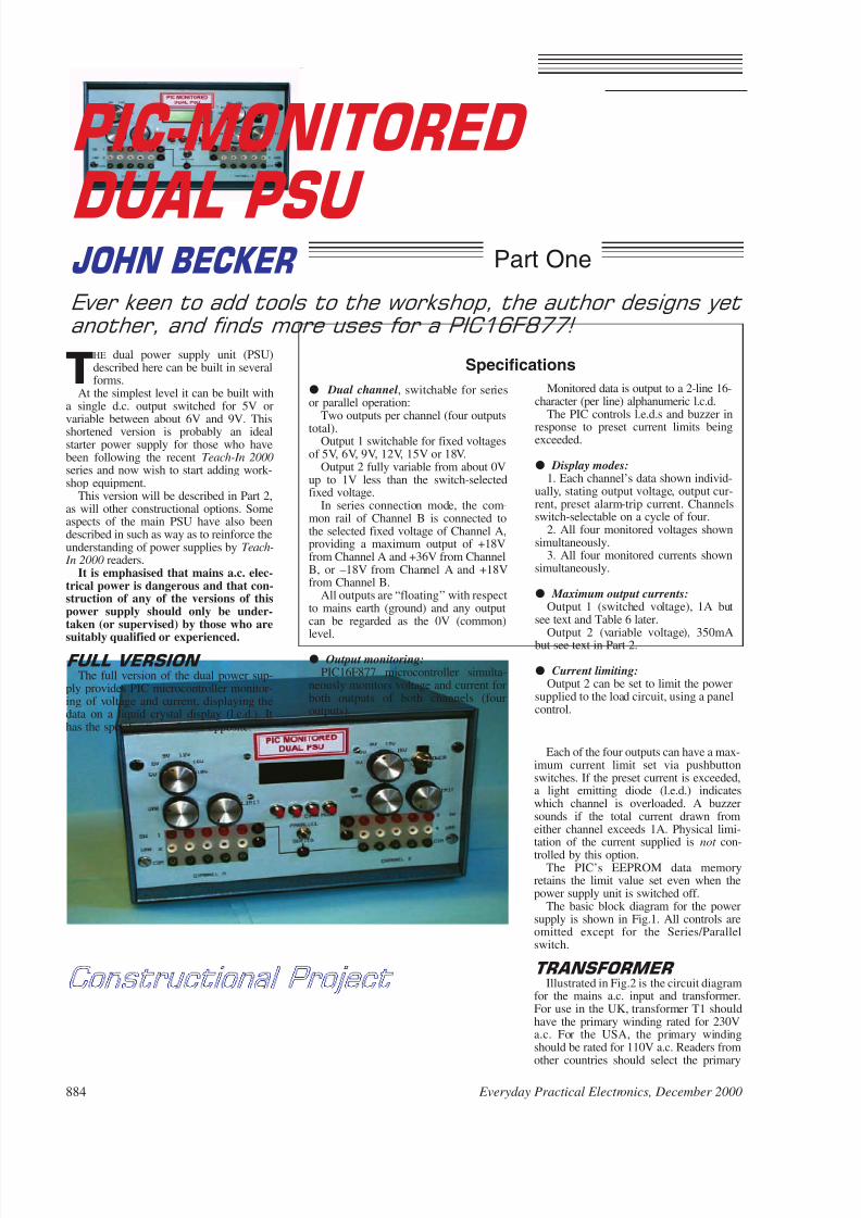
FULL VERSION The full version of the dual power sup-
ply provides PIC microcontroller monitor-ing of voltage and current, displaying thedata on a liquid crystal display (l.c.d.). Ithas the specifications shown opposite.
Each of the four outputs can have a max-imum current limit set via pushbuttonswitches. If the preset current is exceeded,a light emitting diode (l.e.d.) indicateswhich channel is overloaded. A buzzersounds if the total current drawn fromeither channel exceeds 1A. Physical limi-tation of the current supplied is not con-
trolled by this option.The PIC’s EEPROM data memory
retains the limit value set even when thepower supply unit is switched off.
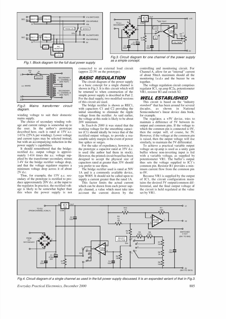
The basic block diagram for the powersupply is shown in Fig.1. All controls areomitted except for the Series/Parallelswitch.
TRANSFORMER Illustrated in Fig.2 is the circuit diagram
for the mains a.c. input and transformer.For use in the UK, transformer T1 shouldhave the primary winding rated for 230Va.c. For the USA, the primary windingshould be rated for 110V a.c. Readers fromother countries should select the primary
PIC-MONITORED
DUAL PSU Ever keen to add tools to the workshop, the author designs yet another, and finds more uses for a PIC16F877!
884 Everyday Practical Electronics, December 2000
JOHN BECKER Part One
Specifications
* Dual channel , switchable for seriesor parallel operation:
Two outputs per channel (four outputs
total).Output 1 switchable for fixed voltages
of 5V, 6V, 9V, 12V, 15V or 18V.Output 2 fully variable from about 0V
up to 1V less than the switch-selectedfixed voltage.
In series connection mode, the com-mon rail of Channel B is connected tothe selected fixed voltage of Channel A,providing a maximum output of +18Vfrom Channel A and +36V from ChannelB, or –18V from Channel A and +18Vfrom Channel B.
All outputs are “floating’’ with respectto mains earth (ground) and any outputcan be regarded as the 0V (common)level.
*Output monitoring:PIC16F877 microcontroller simulta-
neously monitors voltage and current forboth outputs of both channels (fouroutputs).
Monitored data is output to a 2-line 16-character (per line) alphanumeric l.c.d.
The PIC controls l.e.d.s and buzzer in
response to preset current limits beingexceeded.
* Display modes:1. Each channel’s data shown individ-
ually, stating output voltage, output cur-rent, preset alarm-trip current. Channelsswitch-selectable on a cycle of four.
2. All four monitored voltages shownsimultaneously.
3. All four monitored currents shownsimultaneously.
* Maximum output currents:Output 1 (switched voltage), 1A but
see text and Table 6 later.Output 2 (variable voltage), 350mA
but see text in Part 2.
*Current limiting:Output 2 can be set to limit the power
supplied to the load circuit, using a panelcontrol.
7/29/2019 Proyecto 2 Con PIC16F877
http://slidepdf.com/reader/full/proyecto-2-con-pic16f877 3/8
winding voltage to suit their domesticmains supply.
The choice of secondary winding volt-age and current ratings is somewhat up tothe user. In the author’s prototypedescribed here, each is rated at 15V a.c.1·67A (25VA per winding). Lower voltageand current types may be selected instead,but with an accompanying reduction in thepower supply’s capabilities.
It should remembered that the bridge-rectified d.c. output voltage is approxi-mately 1·414 times the a.c. voltage sup-plied by the transformer secondary, minus1·4V for the bridge rectifier voltage drop,and that the voltage regulator requires aminimum voltage drop across it of about2V d.c.
Thus, for example, the 15V a.c. sec-ondary of the prototype is rectified to pro-duce approximately 20V d.c. at the input tothe regulator. In practice, the rectified volt-age is likely to be somewhat higher thanthis when the power supply is not
connected to an external load circuit(approx 22·3V on the prototype).
BASIC REGULATION The circuit diagram of the power supply
as a basic concept for a single channel isshown in Fig.3. It is this circuit which willbe returned to when construction of thesimple power supply is described in Part 2.For the dual supply, two modified versionsof this circuit are used.
The bridge rectifier is shown as REC1,with capacitors C1 and C2 providing the
initial smoothing to eliminate the ripplevoltage from the rectifier. As said earlier,the voltage at this node is likely to be about20V minimum.
In Teach-In 2000 it was stated that theworking voltage for the smoothing capaci-tor (C1) should ideally be twice that of therectified output voltage, to provide a rea-sonable safety margin in the event of powerline spikes or surges.
For the sake of expediency, however, inthe prototype a capacitor rated at 35V d.c.is used (the author had them in stock).However, the printed circuit board has beendesigned to accept the physical size of capacitors rated at greater than 35V shouldyou prefer to use them.
The bridge rectifier used is rated at 50V1A and is a commonly available device,type W005. It should not be called upon tosupply a current greater than the rated 1A.
This factor limits the actual currentwhich can be drawn from each power sup-ply channel, a value which must take intoaccount the current drawn by the
controlling and monitoring circuit. ForChannel A, allow for an “internal’’ currentof about 50mA maximum should all themonitoring l.e.d.s and the buzzer be ontogether.
The voltage regulation circuit comprisesregulator IC1, op.amp IC2a, potentiometerVR1, resistor R1 and switch S2.
WELL ESTABLISHED This circuit is based on the “industry
standard’’ that has been around for severaldecades, as shown in National
Semiconductor’s linear device data book,for example.
The regulator, a +5V device, tries tomaintain a difference of 5V between itsoutput and common pins. If the voltage towhich the common pin is connected is 0V,then the output will, of course, be 5V.However, if the voltage at the common pinis raised, then the output voltage will risesimilarly, to maintain the 5V differential.
To achieve a practical variable outputvoltage an op.amp is used as a unity gainbuffer whose non-inverting input is fedwith a variable voltage, as supplied bypotentiometer VR1. The buffer’s outputthus sets the voltage supplied to IC1’scommon pin. Resistor R1 provides a min-imum current flow from the common pinto 0V.
Because VR1 is supplied by the outputof IC1, the circuit configuration main-tains the desired 5V output/common dif-ferential, and the final output voltage of the circuit is held regulated at the valueset by VR1.
RECT. B PSU BSEC. a.c.
RECT. A PSU A
+5V PICMONITOR
L.C.D.
PARALLEL SERIES
VIa SWITCHED
V2a VARIABLE
V2b VARIABLE
V1b SWITCHED
S7b
0V
V0b
+VE
+VESEC. a.c.
0V
0V
+-
+
VOLTAGE
VAR
5V
COM
OUTIN
SECONDARYTO a.c.
0V
+VE
10kVR1
LM358IC2aS2
100nC3
1kR1
4700µC1
220nC2
REC1
7805IC1
+
**
*SEE TEXT
1
8
4
2
3
FIg.1. Block diagram for the full dual power supply.
Fig.3. Circuit diagram for one channel of the power supply as a simple concept.
SECONDARYa.c. CHANNEL B
SECONDARYa.c. CHANNEL A
(SEE TEXT)
FS11A S1
L
N
E
a.c. MAINS
(SEE TEXT)
ON/OFF
Fig.2. Mains transformer circuit diagram.
+-
+
+
C14700µ
IC17805
R11k
C3100n
S2b
C4100n
C2220n
IN OUT
COM
R21M
C5100n
R43k
620ΩR5
910ΩR6
1k5R7
3kR8
R91k8
S2a
FROMa.c.
SECONDARY
TO IC5(FROM CHANNEL A ONLY)
VOLTAGESELECT
V1
V2
SWITCHEDV OUT
(SK1 TO SK5)
0V(SK11TO SK15)
REC1
+
IC2aLM358
1
8
4
2
3
IC2bLM358
6
5
7
R3
1Ω
R1011k
R11100k
35V
1W
7
8
9
10
1112
1
2
3
4
56
Fig.4. Circuit diagram of a single channel as used in the full power supply discussed. It is an expanded variant of that in Fig.3.
Everyday Practical Electronics, December 2000 885
7/29/2019 Proyecto 2 Con PIC16F877
http://slidepdf.com/reader/full/proyecto-2-con-pic16f877 4/8
It should be noted, though, that theoutput of the op.amp (a type LM358) cannever fall to 0V. More typically theminimum output voltage available willbe about 0·5V. Consequently, the mini-mum regulated voltage that can be set byVR1 will be about 5·5V. The maximumvoltage will about 2V below the rectifiedvoltage fed into the input of regulatorIC1.
In Fig.3, switch S2 selects whether IC1’scommon pin is connected to 0V (for fixed
5V output) or to the op.amp’s output (forvariable voltage control).
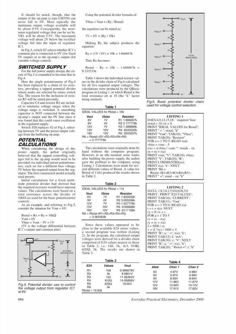
SWITCHED SUPPLY For the full power supply design, the cir-
cuit of Fig.3 is expanded to become that inFig.4.
Here the single potentiometer of Fig.4has been replaced by a chain of six resis-tors, providing a tapped potential dividerwhose nodes are selected by rotary switchS2a. The reason for the inclusion of resis-tor R3 will be stated presently.
Capacitor C4 and resistor R2 are includ-ed to minimise voltage surges when thevoltage range is switched. A smoothingcapacitor is NOT connected between the
op.amp’s output and the 0V line since itwas found that this could cause oscillationin the regulated supply.
Switch S2b replaces S2 of Fig.3, select-ing between 5V and the preset output volt-age from the buffering op.amp.
POTENTIAL
CALCULATIONS When considering the design of this
power supply, the author originallybelieved that the tapped controlling volt-ages fed to the op.amp would need to beprovided via individual preset potentiome-ters, each set for a different bias voltage,5V below the required output from the reg-ulator. The first constructed model actuallyused presets.
Initial calculations for a fixed multi-node potential divider had showed thatthe required resistors would have unusualvalues. The calculations were based on atotal resistance across the divider of 10k W (as used for the basic potentiometercontrol).
As an example, and referring to Fig.5,consider the situation for Vout = 6V:
Rtotal = Rx + Ry = 10k WVout = 6VVbias = Vout – 5V = 1V(5V is the voltage differential between
IC1’s output and common pins)
Using the potential divider formula of:
Vbias = Vout × (Ry / Rtotal)
the equation can be stated as:
1V = 6V × (Ry / 10k)
Making Ry the subject produces theequation:
Ry = (1V / 6V) × 10k = 1·666667k
Thus Rx becomes:
Rtotal – Ry = 10k – 1·666667k =8·333333k
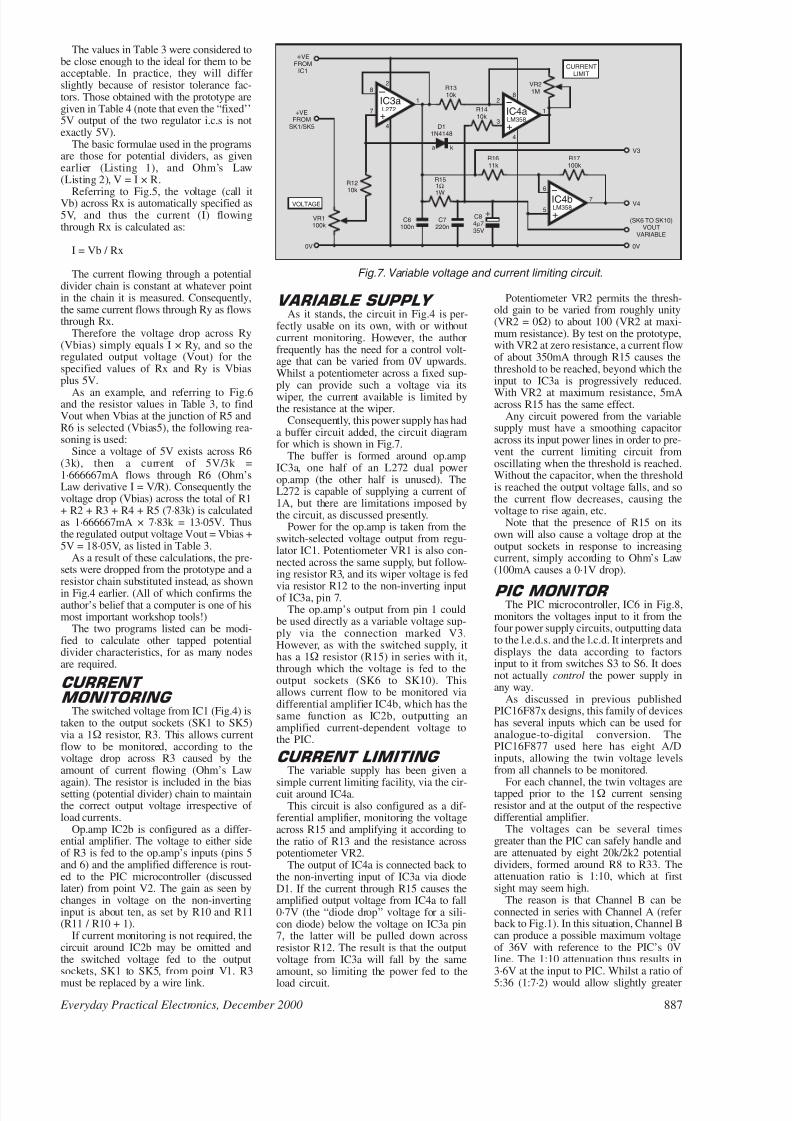
Table 1 shows the individual resistor val-ues in the divider chain of Fig.6 calculatedfor all five required output voltages. Thecalculations were produced by the QBasicprogram in Listing 1, in which Rtotal is thetotal resistance set at 10 (the “k’’ factorbeing omitted).
Table 1
IDEAL VALUES for Rtotal = 10k
Vout Vbias Resistor 6V 1V R1 1·666667k9V 4V R2 2·777778k
12V 7V R3 1·388889k15V 10V R4 ·8333332k18V 13V R5 ·5555557k
R6 = Rtotal–(R1+R2+R3+R4+R5)= 2·777778k
The calculations were originally done byhand without the computer program.However, in an idle moment some weeksafter building the power supply, the authorgave the problem to the computer, usingListing 1. Calculations were made for sev-eral different values of Rtotal. A value forRtotal of 11(k) produced the results shown
in Table 2.
Table 2
IDEAL VALUES for Rtotal = 11k
Vout Vbias Resistor
6V 1V R1 1·833333k9V 4V R2 3·055556k
12V 7V R3 1·527778k15V 10V R4 ·9166668k18V 13V R5 ·6111109k
R6 = Rtotal-(R1+R2+R3+R4+R5)= 3·055555k
Since these values appeared to beclose to the available E24 series values,a second program was written (Listing2). In the program, the calculated outputvoltages were derived for a divider chaincomprised of E24 values nearest to thosein Table 2, i .e. 1k8, 3k, 1k5, 910W,620W, 3k. The results are shown inTable 3.
Table 3
E24 Values Vout
R1 1k8 5·996678VR2 3k 8·9801VR3 1k5 11·95364VR4 910W 14·95856VR5 620W 18·05VR6 3k
Rtotal = 10·83k
Table 4
Ideal Chan 1 Chan 2
5V 4·97V 4·98V6V 5·97V 5·98V9V 8·93V 8·94V12V 11·86V 11·87V15V 14·84V 14·74V18V 17·91V 17·82V
886 Everyday Practical Electronics, December 2000
+
VBIAS
VBIAS
1V
DIFFERENTIAL
5V FIXED
0V
6V
VOUT
1V
OUT
COM
IN
RY
RX
7805
Fig.5. Potential divider use to control the voltage output from regulator IC1
at 6V.
LISTING 1DATA 6,9,12,15,18: ‘ required Voutrtotal = 10: rn = 0PRINT 6IDEAL VALUES for Rtotal6;PRINT 6 = 6; rtotal; 6k 6PRINT 6Vout6; TAB(10); 6Vbias6;PRINT TAB(20); 6Resistor6FOR a = 1 TO 5: READ voutvbias = vout – 5r(a) = ((vbias / vout) * rtotal) – rn.rn = rn + r(a)PRINT vout; 6V6; TAB(10); vbias;PRINT 6V6; TAB(20); 6R6;PRINT LTRIM$(STR$(a));PRINT r(a); 6k 6: NEXTPRINT 6R6 =
Rtotal–(R1+R2+R3+R4+R5)6;
PRINT 6 =6; rtotal – rn; 6k 6
TOTAL
VOUT
R4
R5
R6
VBIAS 3
VBIAS 4
VBIAS 5
RESISTANCE
0V
R1
R2
R3
VBIAS 1
VBIAS 2
Fig.6. Basic potential divider chain used for voltage control selection.
LISTING 2
DATA 1.8,3.0,1.5,910,620,3.0PRINT : PRINT 6E24 VALUES6;PRINT TAB(16); 6CURRENT6;PRINT TAB(31); 6Vout6FOR a = 1 TO 6: READ r(a)t = t + r(a): NEXTry = 0: rx = tFOR a = 1 TO 5rx = rx – r(a)ry = ry + r(a)I = 5000 / rxv = (I *ry) / 1000 + 5
PRINT6R6; a;
6=6; r(a);
6k 6;PRINT TAB(15); I; 6mA6;
PRINT TAB(30); v; 6V6: NEXTPRINT 6R6; a; 6 =6; r(a); 6k 6;PRINT TAB(20); 6 Rtotal =6; t; 6k 6
7/29/2019 Proyecto 2 Con PIC16F877
http://slidepdf.com/reader/full/proyecto-2-con-pic16f877 5/8
Everyday Practical Electronics, December 2000 887
The values in Table 3 were considered tobe close enough to the ideal for them to beacceptable. In practice, they will differslightly because of resistor tolerance fac-tors. Those obtained with the prototype aregiven in Table 4 (note that even the “fixed’’5V output of the two regulator i.c.s is notexactly 5V).
The basic formulae used in the programsare those for potential dividers, as givenearlier (Listing 1), and Ohm’s Law(Listing 2), V = I × R.
Referring to Fig.5, the voltage (call itVb) across Rx is automatically specified as5V, and thus the current (I) flowingthrough Rx is calculated as:
I = Vb / Rx
The current flowing through a potentialdivider chain is constant at whatever pointin the chain it is measured. Consequently,the same current flows through Ry as flowsthrough Rx.
Therefore the voltage drop across Ry(Vbias) simply equals I × Ry, and so theregulated output voltage (Vout) for thespecified values of Rx and Ry is Vbiasplus 5V.
As an example, and referring to Fig.6and the resistor values in Table 3, to findVout when Vbias at the junction of R5 andR6 is selected (Vbias5), the following rea-soning is used:
Since a voltage of 5V exists across R6(3k), then a current of 5V/3k =1·666667mA flows through R6 (Ohm’sLaw derivative I = V/R). Consequently thevoltage drop (Vbias) across the total of R1+ R2 + R3 + R4 + R5 (7·83k) is calculatedas 1·666667mA × 7·83k = 13·05V. Thusthe regulated output voltage Vout = Vbias +5V = 18·05V, as listed in Table 3.
As a result of these calculations, the pre-sets were dropped from the prototype and aresistor chain substituted instead, as shownin Fig.4 earlier. (All of which confirms theauthor’s belief that a computer is one of hismost important workshop tools!)
The two programs listed can be modi-fied to calculate other tapped potentialdivider characteristics, for as many nodesare required.
CURRENT
MONITORING The switched voltage from IC1 (Fig.4) is
taken to the output sockets (SK1 to SK5)via a 19 resistor, R3. This allows currentflow to be monitored, according to thevoltage drop across R3 caused by theamount of current flowing (Ohm’s Law
again). The resistor is included in the biassetting (potential divider) chain to maintainthe correct output voltage irrespective of load currents.
Op.amp IC2b is configured as a differ-ential amplifier. The voltage to either sideof R3 is fed to the op.amp’s inputs (pins 5and 6) and the amplified difference is rout-ed to the PIC microcontroller (discussedlater) from point V2. The gain as seen bychanges in voltage on the non-invertinginput is about ten, as set by R10 and R11(R11 / R10 + 1).
If current monitoring is not required, thecircuit around IC2b may be omitted andthe switched voltage fed to the outputsockets, SK1 to SK5, from point V1. R3
must be replaced by a wire link.
VARIABLE SUPPLY As it stands, the circuit in Fig.4 is per-
fectly usable on its own, with or withoutcurrent monitoring. However, the authorfrequently has the need for a control volt-age that can be varied from 0V upwards.Whilst a potentiometer across a fixed sup-ply can provide such a voltage via itswiper, the current available is limited bythe resistance at the wiper.
Consequently, this power supply has hada buffer circuit added, the circuit diagramfor which is shown in Fig.7.
The buffer is formed around op.ampIC3a, one half of an L272 dual powerop.amp (the other half is unused). TheL272 is capable of supplying a current of 1A, but there are limitations imposed bythe circuit, as discussed presently.
Power for the op.amp is taken from theswitch-selected voltage output from regu-lator IC1. Potentiometer VR1 is also con-nected across the same supply, but follow-ing resistor R3, and its wiper voltage is fed
via resistor R12 to the non-inverting inputof IC3a, pin 7.The op.amp’s output from pin 1 could
be used directly as a variable voltage sup-ply via the connection marked V3.However, as with the switched supply, ithas a 19 resistor (R15) in series with it,through which the voltage is fed to theoutput sockets (SK6 to SK10). Thisallows current flow to be monitored viadifferential amplifier IC4b, which has thesame function as IC2b, outputting anamplified current-dependent voltage tothe PIC.
CURRENT LIMITING The variable supply has been given a
simple current limiting facility, via the cir-cuit around IC4a.This circuit is also configured as a dif-
ferential amplifier, monitoring the voltageacross R15 and amplifying it according tothe ratio of R13 and the resistance acrosspotentiometer VR2.
The output of IC4a is connected back tothe non-inverting input of IC3a via diodeD1. If the current through R15 causes theamplified output voltage from IC4a to fall0·7V (the “diode drop’’ voltage for a sili-con diode) below the voltage on IC3a pin7, the latter will be pulled down acrossresistor R12. The result is that the outputvoltage from IC3a will fall by the sameamount, so limiting the power fed to the
load circuit.
Potentiometer VR2 permits the thresh-old gain to be varied from roughly unity(VR2 = 09) to about 100 (VR2 at maxi-mum resistance). By test on the prototype,with VR2 at zero resistance, a current flowof about 350mA through R15 causes thethreshold to be reached, beyond which theinput to IC3a is progressively reduced.
With VR2 at maximum resistance, 5mAacross R15 has the same effect.
Any circuit powered from the variablesupply must have a smoothing capacitoracross its input power lines in order to pre-vent the current limiting circuit fromoscillating when the threshold is reached.Without the capacitor, when the thresholdis reached the output voltage falls, and sothe current flow decreases, causing thevoltage to rise again, etc.
Note that the presence of R15 on itsown will also cause a voltage drop at theoutput sockets in response to increasingcurrent, simply according to Ohm’s Law(100mA causes a 0·1V drop).
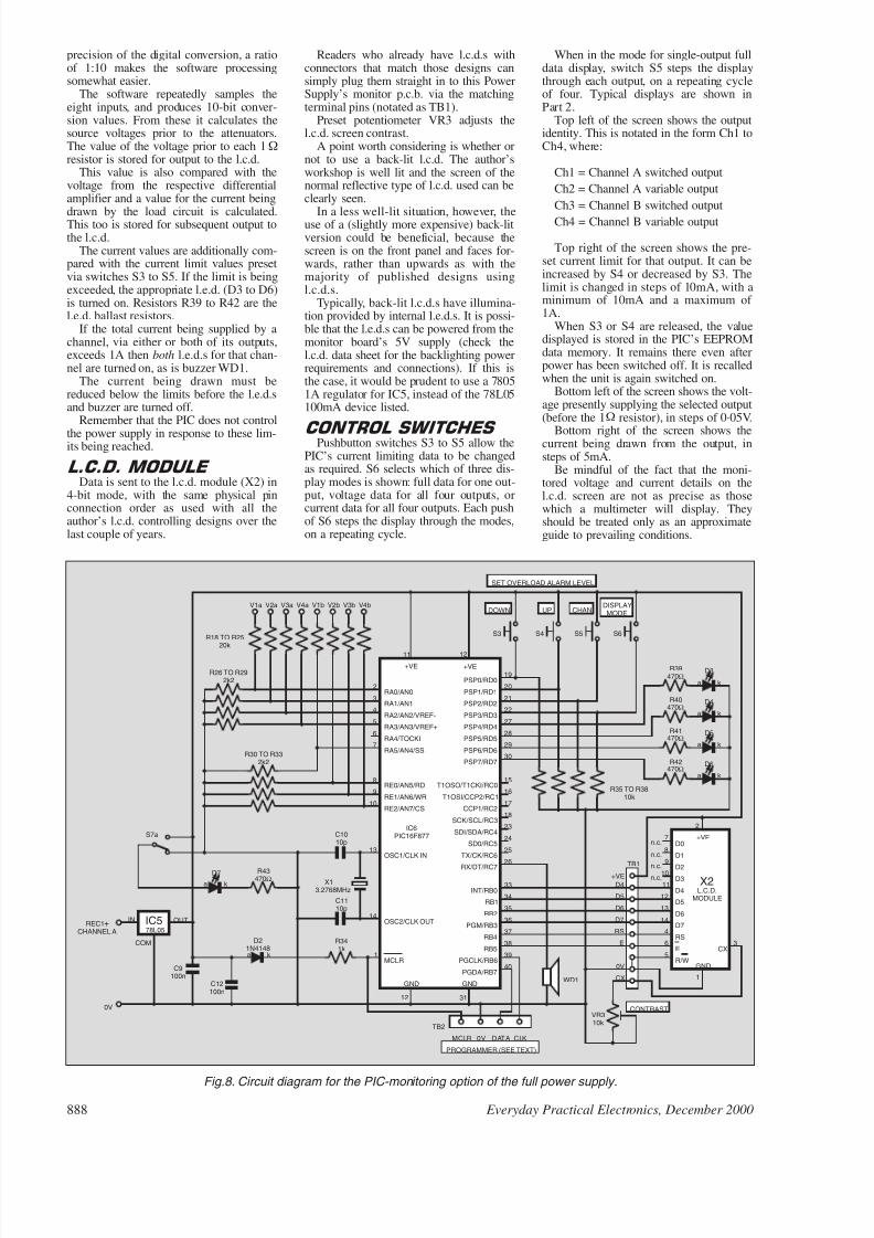
PIC MONITOR The PIC microcontroller, IC6 in Fig.8,
monitors the voltages input to it from thefour power supply circuits, outputting datato the l.e.d.s. and the l.c.d. It interprets anddisplays the data according to factorsinput to it from switches S3 to S6. It doesnot actually control the power supply inany way.
As discussed in previous publishedPIC16F87x designs, this family of deviceshas several inputs which can be used foranalogue-to-digital conversion. ThePIC16F877 used here has eight A/Dinputs, allowing the twin voltage levelsfrom all channels to be monitored.
For each channel, the twin voltages aretapped prior to the 19 current sensingresistor and at the output of the respectivedifferential amplifier.
The voltages can be several timesgreater than the PIC can safely handle andare attenuated by eight 20k/2k2 potentialdividers, formed around R8 to R33. Theattenuation ratio is 1:10, which at firstsight may seem high.
The reason is that Channel B can beconnected in series with Channel A (referback to Fig.1). In this situation, Channel Bcan produce a possible maximum voltageof 36V with reference to the PIC’s 0Vline. The 1:10 attenuation thus results in3·6V at the input to PIC. Whilst a ratio of
5:36 (1:7·2) would allow slightly greater
1
7
8
4
2
1
3
2
4
7
5
6
D11N4148
0V
LIMITCURRENT
VOLTAGE
0V
SK1/SK5FROM
+VE
IC1FROM
+VE
(SK6 TO SK10)
VARIABLEVOUT
V3
V4
100kVR1
R1210k
C84 7µ
C7220n
C6100n
R151Ω
R1611k
R17100k
VR21M
R1410k
R1310k
+
+
+
L272IC3a
8
LM358IC4a
LM358IC4b
+
a k
35V
1W
Fig.7. Variable voltage and current limiting circuit.
7/29/2019 Proyecto 2 Con PIC16F877
http://slidepdf.com/reader/full/proyecto-2-con-pic16f877 6/8
precision of the digital conversion, a ratioof 1:10 makes the software processingsomewhat easier.
The software repeatedly samples theeight inputs, and produces 10-bit conver-sion values. From these it calculates thesource voltages prior to the attenuators.The value of the voltage prior to each 19resistor is stored for output to the l.c.d.
This value is also compared with thevoltage from the respective differentialamplifier and a value for the current being
drawn by the load circuit is calculated.This too is stored for subsequent output tothe l.c.d.
The current values are additionally com-pared with the current limit values presetvia switches S3 to S5. If the limit is beingexceeded, the appropriate l.e.d. (D3 to D6)is turned on. Resistors R39 to R42 are thel.e.d. ballast resistors.
If the total current being supplied by achannel, via either or both of its outputs,exceeds 1A then both l.e.d.s for that chan-nel are turned on, as is buzzer WD1.
The current being drawn must bereduced below the limits before the l.e.d.sand buzzer are turned off.
Remember that the PIC does not control
the power supply in response to these lim-its being reached.
L.C.D. MODULE Data is sent to the l.c.d. module (X2) in
4-bit mode, with the same physical pinconnection order as used with all theauthor’s l.c.d. controlling designs over thelast couple of years.
Readers who already have l.c.d.s withconnectors that match those designs cansimply plug them straight in to this PowerSupply’s monitor p.c.b. via the matchingterminal pins (notated as TB1).
Preset potentiometer VR3 adjusts thel.c.d. screen contrast.
A point worth considering is whether ornot to use a back-lit l.c.d. The author’sworkshop is well lit and the screen of thenormal reflective type of l.c.d. used can beclearly seen.
In a less well-lit situation, however, theuse of a (slightly more expensive) back-litversion could be beneficial, because thescreen is on the front panel and faces for-wards, rather than upwards as with themajority of published designs usingl.c.d.s.
Typically, back-lit l.c.d.s have illumina-tion provided by internal l.e.d.s. It is possi-ble that the l.e.d.s can be powered from themonitor board’s 5V supply (check thel.c.d. data sheet for the backlighting powerrequirements and connections). If this isthe case, it would be prudent to use a 78051A regulator for IC5, instead of the 78L05100mA device listed.
CONTROL SWITCHES Pushbutton switches S3 to S5 allow the
PIC’s current limiting data to be changedas required. S6 selects which of three dis-play modes is shown: full data for one out-put, voltage data for all four outputs, orcurrent data for all four outputs. Each pushof S6 steps the display through the modes,on a repeating cycle.
When in the mode for single-output fulldata display, switch S5 steps the displaythrough each output, on a repeating cycleof four. Typical displays are shown inPart 2.
Top left of the screen shows the outputidentity. This is notated in the form Ch1 toCh4, where:
Ch1 = Channel A switched output
Ch2 = Channel A variable output
Ch3 = Channel B switched output
Ch4 = Channel B variable output
Top right of the screen shows the pre-set current limit for that output. It can beincreased by S4 or decreased by S3. Thelimit is changed in steps of 10mA, with aminimum of 10mA and a maximum of 1A.
When S3 or S4 are released, the valuedisplayed is stored in the PIC’s EEPROMdata memory. It remains there even afterpower has been switched off. It is recalledwhen the unit is again switched on.
Bottom left of the screen shows the volt-age presently supplying the selected output(before the 19 resistor), in steps of 0·05V.
Bottom right of the screen shows thecurrent being drawn from the output, insteps of 5mA.
Be mindful of the fact that the moni-tored voltage and current details on thel.c.d. screen are not as precise as thosewhich a multimeter will display. Theyshould be treated only as an approximateguide to prevailing conditions.
888 Everyday Practical Electronics, December 2000
RA0/AN0
RA1/AN1
RA2/AN2/VREF-
RA3/AN3/VREF+
RA4/TOCKI
RE0/AN5/RD
RE1/AN6/WR
RE2/AN7/CS
OSC1/CLK IN
OSC2/CLK OUT
MCLR
PSP0/RD0
PSP1/RD1
PSP2/RD2
PSP3/RD3
PSP4/RD4
PSP5/RD5
PSP6/RD6
PSP7/RD7
T1OSO/T1CKI/RC0
T1OSI/CCP2/RC1
CCP1/RC2
SCK/SCL/RC3
SDI/SDA/RC4
SD0/RC5
TX/CK/RC6
RX/DT/RC7
INT/RB0
RB1
RB2
PGM/RB3
RB4
RB5
PGCLK/RB6
PGDA/RB7
D0
D1
D2
D3
D4
D5
D6
D7
RS
E
R/W
D4
D5
D6
D7
RS
E
IC6PIC16F877
RA5/AN4/SS
V1a V1bV2a V3a V4a V3bV2b V4b
R39470Ω
470Ω
470Ω
470Ω
R40
R41
R42
MCLR 0V DATA CLK
MODULE
0V
CX
+VE
WD1
VR310k
D3
D4
D5
D6
X13.2768MHz
C1110p
C1010p
1kR34
+VE +VE
C9100n
C12100n
R35 TO R3810k
R26 TO R29
2k2R30 TO R33
2k2
R18 TO R2520k
1N4148D2
IN
COM
OUT
78L05
IC5REC1+CHANNEL A
0V
R43470Ω
D7
S7a
DOWN UP CHANDISPLAY
MODE
S3 S4 S5 S6
GND GND
PROGRAMMER (SEE TEXT)
SET OVERLOAD ALARM LEVEL
2
3
4
5
6
7
8
9
10
11 12
19
20
21
22
27
28
29
30
15
16
17
18
23
24
25
26
33
34
35
36
37
38
39
40
3112
1
14
13
+VE
GND
CX
11
12
13
14
4
6
5
2
1
3
L.C.D.X2
CONTRAST
TB1
TB2
a
a
a
a
a
a
k
k
k
k
k
k
7
8
9
10
n.c.
n.c.
n.c.n.c.
Fig.8. Circuit diagram for the PIC-monitoring option of the full power supply.
7/29/2019 Proyecto 2 Con PIC16F877
http://slidepdf.com/reader/full/proyecto-2-con-pic16f877 7/8
MISCELLANY The PIC and l.c.d. are powered at 5V.
This is provided by regulator IC5, whoseinput is connected directly to the rectifiedvoltage at capacitor C1 (approximately20V) of Channel A. The current drawn,with the l.e.d.s inactive, is a little under6mA.
Crystal X1 sets the PIC’s clock frequen-cy at 3·2768MHz.
Selection of parallel or serial connectionof Channels A and B is made by switchS7b in Fig.1 earlier. In Fig.8, S7a is thesecond half of the same switch and turnson l.e.d. D7 when the channels are con-nected in series.
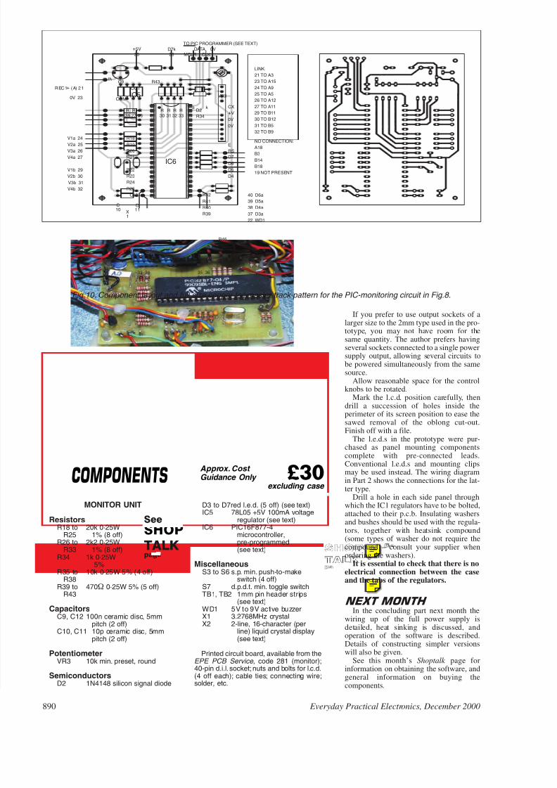
CONSTRUCTION There are two printed circuit boards, one
for the PIC monitoring circuit, the otherfor the power supply components of a sin-gle channel (two are needed if both chan-nels are required).
Their constructional and track layoutdetails are shown in Fig.9 and Fig.10. Theboards are available from the EPE PCBService, code 281 for the monitor and 280for the power supply.
Preferably assemble the components inascending order of size, commencing withthe on-board link wires. Use sockets forIC2, IC3, IC4 and IC6. Do not insert IC6(the PIC) into its socket until a few circuit
tests have been made later. Ensure the cor-rect orientation of all other semiconductorsand the electrolytic capacitors.
Mount the rectifier (REC1) and 1Wresistors (R3 and R15) so that their bodiesstand a bit above the p.c.b., allowing air tocirculate around them. Also mount regula-tor IC1 somewhat above the p.c.b. to allowit to be easily bolted to the side of the caseduring the final stages of connecting up.
For terminal pin blocks TB1 and TB2use 1mm pin-header strips. For the otheroff-board connection points insert 1mmterminal pins.
CASE PREPARATION
The case used in the prototype andshown in the photographs is one which theauthor has had for some years. Regrettablyit has been discontinued by the supplier,but an alternative case of a similar size isquoted in Shoptalk . The size of the originalis 255mm × 160mm × 196mm (l × h × d).The detachable front and rear panels mea-sure 245mm × 135mm. They are madefrom aluminium, whilst the rest of the caseis mild steel.
Referring to the photographs, plan anddrill your chosen case with care. Allowample clearance between all mains pow-ered connections and other items. Use aclamping cable grommet for the mainsinput lead.
Everyday Practical Electronics, December 2000 889
REC1
C1
IC1
IC5
IN
COM
OUT
R3 R15
IC2 IC3IC4
C2
R1
C3
R2
C4
R11 C
5
R10
C6
R12
R13
D1
R14
C7 C8
R16
R17
a k
+
+
+
1 2
V a.c.SECONDARY
3(CHAN. AONLY)
4 5
VOUT(SWITCHED)
VOUT(VARIABLE)V3 VR2 VR2w
6 7 8 9V4
1516170V0VS2b/p
121314S2a/p V2S2b/8 TO 12
101811V1 n .c .VR1w
Fig.9. Printed circuit board component layout and full size copper foil master track pattern for the power supply in Fig.4.
Approx. Cost Guidance Only £30
excluding case
SINGLE FULL PSU CHANNELExcluding the PIC monitoring circuit
ResistorsR1 1k 0·25W 5%R2 1M 0·25W 5%R3, R15 1W 1W 5% (or
better)
(2 off)R4, R8 3k 0·25W 1% (2 off)R5 620W 0·25W 1%R6 910W 0·25W 1%R7 1k5 0·25W 1%R9 1k8 0·25W 1%R10, R16 11k 0·25W 1% (2 off)R11, R17 100k 0·25W 1% (2 off)R12 to 10k 0·25W 5%
R14 (3 off)
PotentiometersVR1 100k lin rotaryVR2 1M lin rotary
CapacitorsC1 4700 mF radial elect.
(see text)C2, C7 220n ceramic disc, 5mmpitch (2 off)
C3 to C6 100n ceramic disc, 5mmpitch (4 off)
C8 4 m7 radial elect. 35V
SemiconductorsD1 1N4148 silicon signal diodeIC1 7805 +5V 1A voltage
regulatorIC2, IC4 LM358 dual op.amp (2 off)IC3 L272 dual power op.amp
MiscellaneousREC1 W005 50V 1A bridge
rectifier, or similar
S1 s.p.d.t. switch, mains ratedS2 2-pole 6-way rotary switchSK1 to 2mm socket, 3 colours,
SK15 5 off each (see text)
Printed circuit board (power supply),available from the EPE PCB Service code 280; knob (3 off); TO220 insulatingwasher kit for IC1; 8-pin d.i.l. socket(3 off)All above parts repeated for second channel.
Also requiredFS1 20mm fuseholder, panel
mounting, with 1A 20mmfuse, slow blow
T1 mains transformer, 0-15V,0-15V secondaries, 50VA(25VA per winding)
Metal case, 255mm × 160mm ×196mm (see text); heatsink compound(see text); eyelet tag; mains cableclamping grommet; nuts and bolts formounting transformer (2 off each); cableties; 1mm terminal pins; 3-core mainscable, 5A; connecting wire; solder, etc
COMPONENTS
SeeSHOPTALK page
7/29/2019 Proyecto 2 Con PIC16F877
http://slidepdf.com/reader/full/proyecto-2-con-pic16f877 8/8
If you prefer to use output sockets of alarger size to the 2mm type used in the pro-totype, you may not have room for thesame quantity. The author prefers havingseveral sockets connected to a single powersupply output, allowing several circuits tobe powered simultaneously from the samesource.
Allow reasonable space for the controlknobs to be rotated.
Mark the l.c.d. position carefully, thendrill a succession of holes inside the
perimeter of its screen position to ease thesawed removal of the oblong cut-out.Finish off with a file.
The l.e.d.s in the prototype were pur-chased as panel mounting componentscomplete with pre-connected leads.Conventional l.e.d.s and mounting clipsmay be used instead. The wiring diagramin Part 2 shows the connections for the lat-ter type.
Drill a hole in each side panel throughwhich the IC1 regulators have to be bolted,attached to their p.c.b. Insulating washersand bushes should be used with the regula-tors, together with heatsink compound(some types of washer do not require thecompound – consult your supplier whenordering the washers).
It is essential to check that there is noelectrical connection between the caseand the tabs of the regulators.
NEXT MONTH In the concluding part next month the
wiring up of the full power supply isdetailed, heat sinking is discussed, andoperation of the software is described.Details of constructing simpler versionswill also be given.
See this month’s Shoptalk page forinformation on obtaining the software, andgeneral information on buying thecomponents.
890 Everyday Practical Electronics, December 2000
R29
R28
R27
R26
R30
R31
R32
R33 R34
D2a k
IC5
R43C9
COM
IN
OUT
R18R19
R20
R21
R22
R23
R24
R25
C12
C11
C10
X1
IC6
R43
R44
R42
R41
R40
R39
R46
R45
VR3
40 D6a
39 D5a
38 D4a
37 D3a
22 WD1
V1a 24V2a 25
V3a 26
V4a 27
V1b 29
V2b 30
V3b 31
V4b 32
REC1 (A) 21+
0V 23
+5V
20D7k28
CX
+V
0V
0V
E
RS
D7
D6
D5
D4
33
S3
34
S4
35
S5
36
S6
MCLR
DATA
CLK
0V
TO PIC PROGRAMMER (SEE TEXT)
LINK:
21 TO A3
23 TO A15
24 TO A9
25 TO A5
26 TO A12
27 TO A11
29 TO B11
30 TO B12
31 TO B5
32 TO B9
NO CONNECTION:
A18
B3
B14
B18
19 NOT PRESENT
Fig.10. Component layout and full size copper foil master track pattern for the PIC-monitoring circuit in Fig.8.
Approx. Cost Guidance Only £30
excluding case COMPONENTS
MONITOR UNIT
ResistorsR18 to 20k 0·25W
R25 1% (8 off)R26 to 2k2 0·25W
R33 1% (8 off)R34 1k 0·25W5%
R35 to 10k 0·25W 5% (4 off)R38
R39 to 470W 0·25W 5% (5 off)R43
CapacitorsC9, C12 100n ceramic disc, 5mm
pitch (2 off)C10, C11 10p ceramic disc, 5mm
pitch (2 off)
PotentiometerVR3 10k min. preset, round
SemiconductorsD2 1N4148 silicon signal diode
D3 to D7red l.e.d. (5 off) (see text)IC5 78L05 +5V 100mA voltage
regulator (see text)IC6 PIC16F877-4
microcontroller,pre-programmed
(see text)
MiscellaneousS3 to S6 s.p. min. push-to-make
switch (4 off)S7 d.p.d.t. min. toggle switchTB1, TB2 1mm pin header strips
(see text)WD1 5V to 9V active buzzerX1 3.2768MHz crystalX2 2-line, 16-character (per
line) liquid crystal display(see text)
Printed circuit board, available from theEPE PCB Service , code 281 (monitor);40-pin d.i.l.socket;nuts and bolts for l.c.d.(4 off each); cable ties; connecting wire;solder, etc.
SeeSHOP
TALK page