lecture 06 transistorremodel
TRANSCRIPT
© Copy Right: Rai University4A.273 15
ELECTR
ON
IC D
ESIGN
TECH
NO
LOG
Y
Objective:To understand the transistor re model (CE configuration).A very good morning to all of you! Well students you havealready started a journey in the world of electronics and I amhere to cover some of the milestones with you and guide youin every way possible by this time you are well versed with thebasic concepts like intrinsic, extrinsic semiconductors, diodemechanism, transistor action and much such related topics,which your have studied in basic electronics and solid statedevices and circuits. Believe me students, if your these threesubjects i.e. basic electronics, solid state devices and EDLC areclear and your logics are clear your journey throughout thiselectronics engineering is going to be a very smooth one.You are aware with the basic construction, appearance andcharacteristics of transistor. Name what we have to firstlyunderstand is the small-signal ac response of the BJT amplifierby reviewing the models most frequently used to represent thetransistor in the sinusoidal domain.One of our first concerns in the sinusoidal ac analysis oftransistor n/w is the magnitude of the input signal willdetermine where small signal or large signal techniques shouldbe applied. There is no set dividing line between the two, butthe application and the magnitude of the variables of interestrelative to the scales of the devices characteristics, will usuallymake it quite clear which method is appropriate. Well firstly Iwill try to make you understand the small-scale technique andonce the base is formed we can move over to large-scaleapplications:One thing you have to understand is that the input signal Vi isapplied to the base of the transistor while the output current I 0
is the collector current. The small signal ac analysis begins byremoving the dc effects of Vcc and replacing the dc blockingcapacitors by short circuit equivalents.The key to transistor small signal analysis is the use ofequivalent circuits (models) to be introduced in thischapter.Slant A model is the combination ofcircuit elements, properly chosen, thatbest approximates the actual behaviorof a semiconductor device underspecific operating conditions.
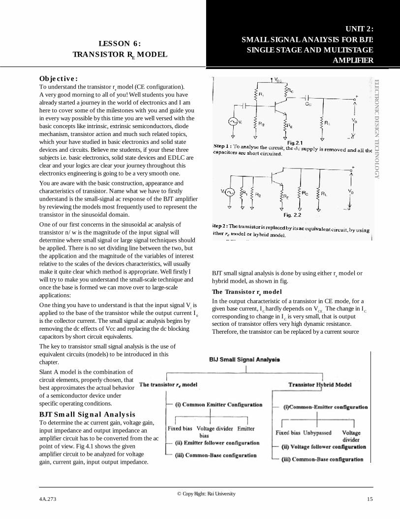
BJT Small Signal AnalysisTo determine the ac current gain, voltage gain,input impedance and output impedance anamplifier circuit has to be converted from the acpoint of view. Fig 4.1 shows the givenamplifier circuit to be analyzed for voltagegain, current gain, input output impedance.
BJT small signal analysis is done by using either re model orhybrid model, as shown in fig.
The Transistor re modelIn the output characteristic of a transistor in CE mode, for agiven base current, IC hardly depends on VCE . The change in IC
corresponding to change in IC is very small, that is outputsection of transistor offers very high dynamic resistance.Therefore, the transistor can be replaced by a current source
UNIT 2: SMALL SIGNAL ANALYSIS FOR BJT:
SINGLE STAGE AND MULTISTAGEAMPLIFIER
LESSON 6:TRANSISTOR RE MODEL
16 4A.273© Copy Right: Rai University
ELECTR
ON
IC D
ESIGN
TECH
NO
LOG
Y
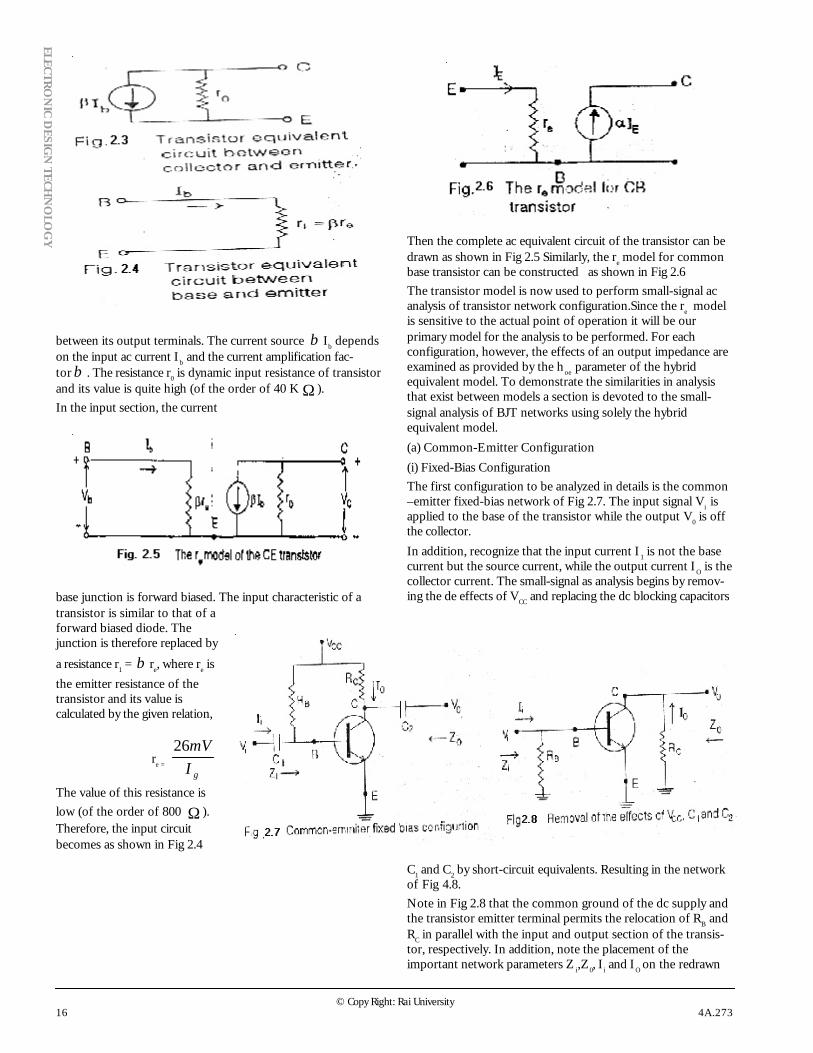
between its output terminals. The current source β Ib dependson the input ac current Ib and the current amplification fac-tor β . The resistance r0 is dynamic input resistance of transistorand its value is quite high (of the order of 40 K Ω ).In the input section, the current
base junction is forward biased. The input characteristic of atransistor is similar to that of aforward biased diode. Thejunction is therefore replaced by
a resistance r1 = β re, where re isthe emitter resistance of thetransistor and its value iscalculated by the given relation,
re = gImV26
The value of this resistance islow (of the order of 800 Ω ).Therefore, the input circuitbecomes as shown in Fig 2.4
Then the complete ac equivalent circuit of the transistor can bedrawn as shown in Fig 2.5 Similarly, the re model for commonbase transistor can be constructed as shown in Fig 2.6The transistor model is now used to perform small-signal acanalysis of transistor network configuration.Since the re modelis sensitive to the actual point of operation it will be ourprimary model for the analysis to be performed. For eachconfiguration, however, the effects of an output impedance areexamined as provided by the h oe parameter of the hybridequivalent model. To demonstrate the similarities in analysisthat exist between models a section is devoted to the small-signal analysis of BJT networks using solely the hybridequivalent model.(a) Common-Emitter Configuration(i) Fixed-Bias ConfigurationThe first configuration to be analyzed in details is the common–emitter fixed-bias network of Fig 2.7. The input signal Vi isapplied to the base of the transistor while the output V0 is offthe collector.In addition, recognize that the input current I 1 is not the basecurrent but the source current, while the output current IO is thecollector current. The small-signal as analysis begins by remov-ing the de effects of VCC and replacing the dc blocking capacitors
C1 and C2 by short-circuit equivalents. Resulting in the networkof Fig 4.8.Note in Fig 2.8 that the common ground of the dc supply andthe transistor emitter terminal permits the relocation of RB andRC in parallel with the input and output section of the transis-tor, respectively. In addition, note the placement of theimportant network parameters Z i,Z0, I i and IO on the redrawn
© Copy Right: Rai University4A.273 17
ELECTR
ON
IC D
ESIGN
TECH
NO
LOG
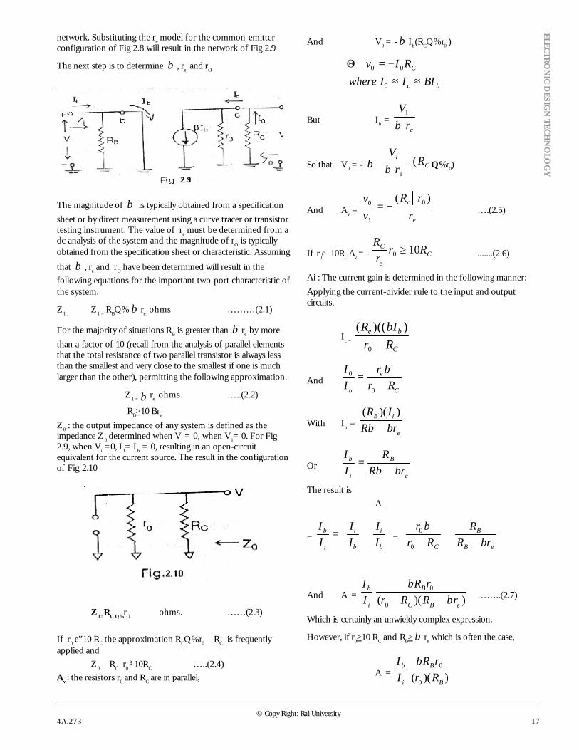
Ynetwork. Substituting the re model for the common-emitterconfiguration of Fig 2.8 will result in the network of Fig 2.9
The next step is to determine β , re,, and rO.
The magnitude of β is typically obtained from a specificationsheet or by direct measurement using a curve tracer or transistortesting instrument. The value of re must be determined from adc analysis of the system and the magnitude of rO is typicallyobtained from the specification sheet or characteristic. Assuming
that β , re and rO have been determined will result in thefollowing equations for the important two-port characteristic ofthe system.
Z1 : Z1 = RBQ% β re ohms ………(2.1)
For the majority of situations RB is greater than β re by morethan a factor of 10 (recall from the analysis of parallel elementsthat the total resistance of two parallel transistor is always lessthan the smallest and very close to the smallest if one is muchlarger than the other), permitting the following approximation.
Z1 = β re ohms …..(2.2)
RB>10 Bre
Z0 : the output impedance of any system is defined as theimpedance Z 0 determined when Vi = 0, when V1= 0. For Fig2.9, when Vi =0, I1= Ib = 0, resulting in an open-circuitequivalent for the current source. The result in the configurationof Fig 2.10
Z0 : RC Q%rO ohms. ……(2.3)
If r0 e”10 RC the approximation RCQ%r0 ≅ RC is frequentlyapplied and
Z0 ≅ RC r0 ³ 10RC …..(2.4)Av : the resistors r0 and RC are in parallel,
And V0 = - β Ib(RCQ%r0 )
≈≈
−=
bc
C
BIIIwhere
RIv
0
00Θ
But Ib = cr
Vβ
1
So that V0 = - β Ce
i Rr
V(
β Q%r0)
And Av = e
c
r
rR
vv )( 0
1
0 −= ….(2.5)
If r0e10RC Av = - Ce
C RrrR
100 ≥ .......(2.6)
Ai : The current gain is determined in the following manner:Applying the current-divider rule to the input and outputcircuits,
Ic =
C
be
RrIR
+0
))((( β
AndC
e
b Rrr
II
+=
0
0 β
With Ib = e
iB
rRIRββ +
))((
Or =i
b
II
e
B
rRR
ββ +
The result isAi
= =i
b
II
b
i
II
b
i
II
=
+ CRrr
0
0 β
+ eB
B
rRR
β
And Ai = i
b
II
))(( 0
0
eBC
B
rRRrrR
ββ
++ ……..(2.7)
Which is certainly an unwieldy complex expression.
However, if r0>10 RC and RB> β re which is often the case,
Ai = i
b
II
))(( 0
0
B
B
RrrRβ
18 4A.273© Copy Right: Rai University
ELECTR
ON
IC D
ESIGN
TECH
NO
LOG
Y
And A1 ≅ β r0e”10 RC, RB e”10 β re ……(2.8)
The complexity of Eq. (4.7) suggests that we may want toreturn to an equation such as eq. (4.10), which utilizes A0 and Z ithat is
A1 = C
v
RZA 1
…..(2.9)
Phase RelationshipThe negative sign in the resulting equation for Av reveals that a1800 phase shift occurs between the input and output signals, asshown in fig 2.11
Example.1: for the network of Fig 2.12:
(a) Determine re
(b)Find Z i (with r0 = Ω∞ )(c) Calculate Z0 (with r0 = Ω∞ )(d)Determine Av (with r0= Ω∞ )(e) Find Ai (with r0 = Ω∞ )(f) Repeat parts (c) through (e) including r0 = 50 K Ω in all
calculation and compare results.Solution:
(a)DC analysis:
IB= AK
VVR
VV
B
BEcc µ04.24470
7.012=
Ω−
=−
IE = ( β +1)IB = (101)(24.14 Aµ )=2.428 mA
re = =EImV26
Ω= 71.10428.226
mAmV
(b) Ω=ΩΩ==
Ω=
KKKrRZ
r
eBi
e
069.1071.1470
)71.10)(100(
β
β
(c) Z0 = RC = 3 K Ω
(d) Av = 11.28071.10
3−=
ΩΩ
−=K
rR
e
C
(e) Since RB>10 β re (470 k Ω >1071K Ω )
Ai 100β≅
(f) Including r0 = 50 k Ω : Z0=r0Q%RC = 50K Ω Q%3K
Ω = 2.83 K Ω vs 3K Ω
Av = 11.28024.264.71.10
83.20 −=ΩΩ
= vsK
r
Rr
e
C
Ai = ))(( 0
0
eBC
B
rRRrrR
ββ
++
= 100.13.94)071.1470)(350(
)50()047)(100(vs
kkkkkk
=Ω+ΩΩ+Ω
ΩΩ
As a check:
Ai = -Av 16.943
)069.1)(24.264(=
ΩΩ−−
=k
kRZ
C
i
Which differs slightly only due to the accuracy carried throughthe calculation.(ii) Voltage –Divider BiasThe next configuration to be
© Copy Right: Rai University4A.273 19
ELECTR
ON
IC D
ESIGN
TECH
NO
LOG
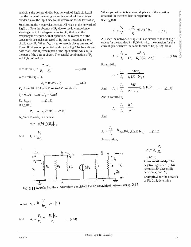
Yanalysis is the voltage-divider bias network of Fig 2.13. Recallthat the name of the configuration is a result of the voltage-divider bias at the input side to the determine the dc level of VB.Substituting the re equivalent circuit will result in the network ofFig 2.14. Note the absence of RE due to the low-impedanceshorting effect of the bypass capacitor, CE. that is, at thefrequency (or frequencies) of operation, the reactance of thecapacitor is so small compared to RE that is treated as a shortcircuit across RE. When VCC is set to zero, it places one end ofR1 and RC at ground potential as shown in Fig 2.14. In addition,note that R1and R2 remain part of the input circuit while RC isthe part of the output circuit. The parallel combination of R1
and R2 is defined by
R’ = R1Q%R2 = 21
21
RRRR
+ ….(2.10)
Zi = From Fig 2.14,
Zi = R’Q% β re …….(2.11)
Z0 : From Fig 2.14 with Vi set to 0 V resulting in
Ib = 0 mAIandA b 0=βµ
Z0 = RC Q%r0 ….(2.12)If r0>10RC
Z0 CR≅ r0 e”10RC …..(2.13)
Av : Since RC and r0 in a parallel
V0 = - ( 0)(( rRI Cbβ
And Ib = e
i
rVβ
So that V0 = )( 0rRr
VC
e
i
β
β
And Av = 0
0
1
0
r
rR
VV C−= ……(2.14)
Which you will note is an exact duplicate of the equationobtained for the fixed-bias configuration.For r0 >10 RC
Av = CC Rr
rR
VV
10001
0 ≥−≅ …(2.15)
A1: Since the network of Fig 2.14 is so similar to that of Fig 2.3except for the fact that R’=R1Q%R2 =RB , the equation for thecurrent gain will have the same format as Eq. (2.13) that is,
Av = )')(('
0
00
eCi rRRrrR
II
ββ
++= …. (2.16)
For r0>10RC
Ai = )'('
0
00
ei rRrrR
II
ββ
+≅
And Ai = Cei
RrrR
RII
10'
'0
0 ≥+
≅β
β……..(2.17)
And if Re”10 β re,
Ai = ''0
RR
II
i
β≅
And
Av = β≅iI
I 0r0>10RC ,R’>10 β re, …(2.18)
As an option,
A ==-Av CR
Z1
…(2.19)Phase relationship: Thenegative sign of eq. (2.14)reveals a 1800 phase shiftbetween V0 and Vi.
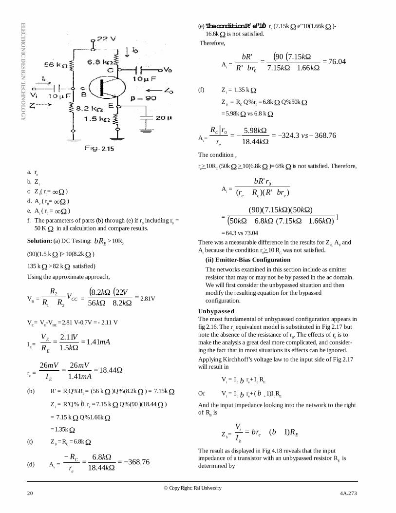
Example.2: for the networkof Fig 2.15, determine
20 4A.273© Copy Right: Rai University
ELECTR
ON
IC D
ESIGN
TECH
NO
LOG
Y
a. re
b. Zi
c. Z0( r0= Ω∞ )d. Av ( r0= Ω∞ )e. Ai ( r0 = Ω∞ )f. The parameters of parts (b) through (e) if r0 including r0 =
50 K Ω in all calculation and compare results.
Solution: (a) DC Testing: ERβ >10R2
(90)(1.5 k Ω )>10(8.2k Ω )
135 k Ω >82 k Ω satisfied)
Using the approximate approach,
VB = CCVRR
R
21
2
+ = ( )( )
=Ω+Ω
ΩkkVk
2.856222.8
2.81V
VE= VB-VBE =2.81 V-0.7V =- 2.11 V
IE= mAkV
RV
E
E 41.15.111.2
=Ω
=
re = Ω== 44.1841.1
2626mA
mVImV
E
(b) R’ = R1Q%R2 = (56 k Ω )Q%(8.2k Ω ) = 7.15k ΩZi = R’Q% β re =7.15 k Ω Q%(90 )(18.44 Ω )
= 7.15 k Ω Q%1.66k Ω=1.35k Ω
(c) Z0 =RC =6.8k Ω
(d) Av = 76.36844.188.6
−=Ω
Ω=
−k
krR
e
C
(e)The condition R’ e”10β re (7.15k Ω e”10(1.66k Ω )-16.6k Ω is not satisfied.
Therefore,
Ai = ( )( )
04.7666.115.7
15.790'
'
0
=Ω+Ω
Ω=
+ kkk
rRRβ
β
(f) Zi = 1.35 k ΩZ0 = RC Q%r0 =6.8k Ω Q%50k Ω=5.98k Ω vs 6.8 k Ω
Av= 76.3683.32444.18
98.50 −−=Ω
Ω−= vs
kk
r
rR
e
C
The condition ,
re>10RC (50k Ω >10(6.8k Ω )=68k Ω is not satisfied. Therefore,
Ai = )')((' 0
ece rRRrrR
ββ
++
= ( ) )66.115.7(8.650)50)(15.7)(90(
Ω+ΩΩ+ΩΩΩ
kkkkkk
]
=64.3 vs 73.04There was a measurable difference in the results for Z 0, AV andAi because the condition r0>10 RC was not satisfied.
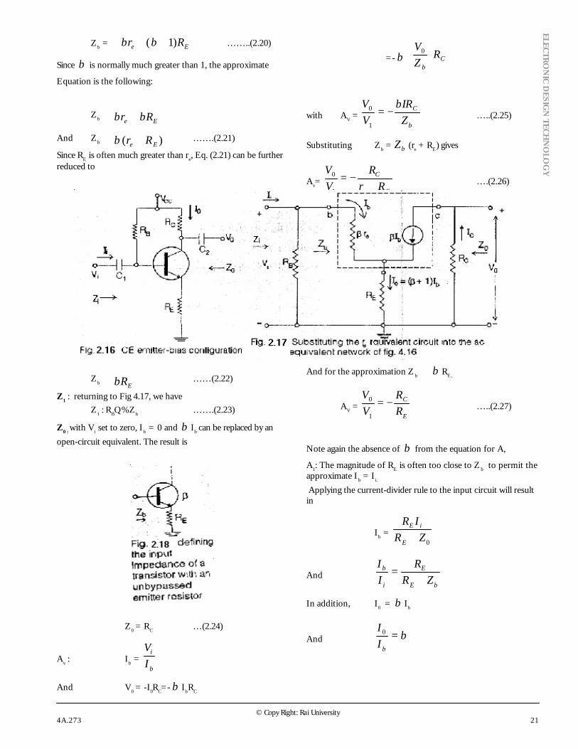
(ii) Emitter-Bias ConfigurationThe networks examined in this section include as emitterresistor that may or may not be by passed in the ac domain.We will first consider the unbypassed situation and thenmodify the resulting equation for the bypassedconfiguration.
UnbypassedThe most fundamental of unbypassed configuration appears infig 2.16. The re equivalent model is substituted in Fig 2.17 butnote the absence of the resistance of r0. The effects of r0 is tomake the analysis a great deal more complicated, and consider-ing the fact that in most situations its effects can be ignored.Applying Kirchhoff’s voltage law to the input side of Fig 2.17will result in
Vi = Ib β re+Ie RE
Or Vi = Ib β re+( β +1)IbRE
And the input impedance looking into the network to the rightof RB is
Zb= Eeb
i RrIV
)1( ++= ββ
The result as displayed in Fig 4.18 reveals that the inputimpedance of a transistor with an unbypassed resistor RE isdetermined by
© Copy Right: Rai University4A.273 21
ELECTR
ON
IC D
ESIGN
TECH
NO
LOG
YZb = Ee Rr )1( ++ ββ ……..(2.20)
Since β is normally much greater than 1, the approximate
Equation is the following:
Zb ≅ Ee Rr ββ +
And Zb ≅ )( Ee Rr +β …….(2.21)
Since RE is often much greater than re, Eq. (2.21) can be furtherreduced to
Zb ≅ ERβ ……(2.22)
Z1 : returning to Fig 4.17, we haveZ1 : RBQ%Zb …….(2.23)
Z0 : with Vi set to zero, Ib = 0 and β Ib can be replaced by anopen-circuit equivalent. The result is
Z0 = RC …(2.24)
Av : Ib = b
i
IV
And V0 = -I0RC=- β IbRC
=- β Cb
RZV
0
with AV = b
C
ZIR
VV β
−=1
0…..(2.25)
Substituting Zb = bZ (re + RE) gives
Av= Ee
C
RrR
VV
+−=
1
0….(2.26)
And for the approximation Z b ≅ β RE,
AV = E
C
RR
VV
−=1
0…..(2.27)
Note again the absence of β from the equation for A,
A1: The magnitude of RE is often too close to Z b to permit theapproximate I b = I i.
Applying the current-divider rule to the input circuit will resultin
Ib = 0ZR
IR
E
iE
+
And =i
b
II
bE
E
ZRR+
In addition, I0 = β Ib
And β=bI
I 0
22 4A.273© Copy Right: Rai University
ELECTR
ON
IC D
ESIGN
TECH
NO
LOG
Y
So that Ai = iI
I 0=
bII 0
i
b
II
= βbE
E
ZRR+
And Ai = iI
I 0=
bE
E
ZRR+
β……(2.28)
Or Ai= -Av
cRZi
……(2.29)
Phase Relationship :The negative sign in equation 2.25 again reveals a 1800 phaseshift between V0 and Vi
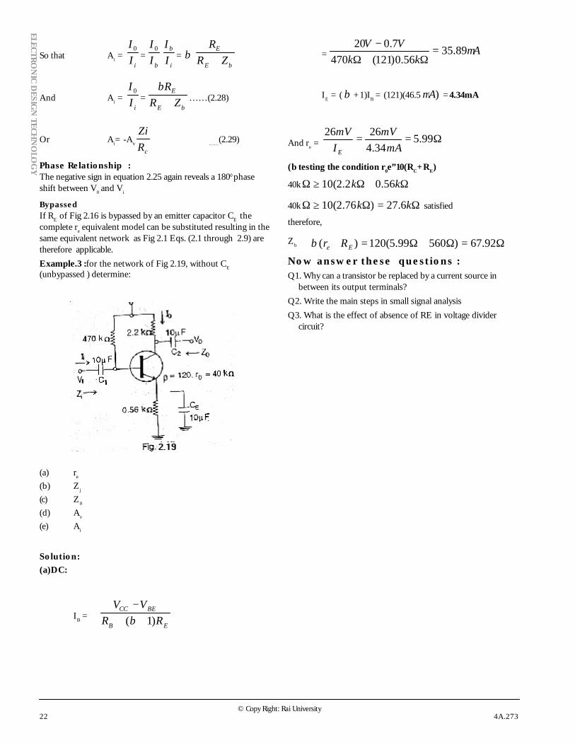
BypassedIf RE of Fig 2.16 is bypassed by an emitter capacitor CE thecomplete re equivalent model can be substituted resulting in thesame equivalent network as Fig 2.1 Eqs. (2.1 through 2.9) aretherefore applicable.Example.3 :for the network of Fig 2.19, without CE(unbypassed ) determine:
(a) re
(b) Zj
(c) Z0
(d) Av
(e) Ai
Solution:(a)DC:
IB = EB
BECC
RRVV
)1( ++−β
= Akk
VVµ89.35
56.0)121(4707.020
=Ω+Ω
−
IE = ( β +1)IB = (121)(46.5 )Aµ =4.34mA
And re = Ω== 99.534.4
2626mA
mVImV
E
(b testing the condition r 0e”10(RC+RE)
40k Ω+Ω≥Ω kk 56.02.2(10
40k Ω=Ω≥Ω kk 6.27)76.2(10 satisfied
therefore,
Zb ≅ Ω=Ω+Ω=+ 92.67)56099.5(120)( Ee Rrβ
Now answer these questions :Q1. Why can a transistor be replaced by a current source in
between its output terminals?Q2. Write the main steps in small signal analysisQ3. What is the effect of absence of RE in voltage divider
circuit?