dmsiÓn de ciencias bÁsicas e ingenierÍa …148.206.53.84/tesiuami/uam4107.pdf · con...
TRANSCRIPT
Casa abierta al tiempo UNIVERSIDAD AUTONOMA METROPOLITANA 1-
DMSIÓN DE CIENCIAS BÁSICAS E INGENIERÍA DEPARTAMENTO DE INGENIERÍA ELÉCTRICA
SISTEMA ULTRASóNICO PARA APOYO DE LA DOCENCIA
REPORTE FINAL DE SEMINARIO DE PROYECTO I Y I1
LÓPEZ DÁVILA IGNACIO CARRANZA PALACIOS ULISES
ASESOR: DIPL. ING. ENRIQUE HERNÁNDEZ MATOS

CONTENIDO
INTRODUCCI~N .......................................................................................................................... 2
DESCRIPCIóN DEL SISTEMA .................................................................................................. 3
OBJETIVOS ................................................................................................................................... 4
DESARROLLO .............................................................................................................................. 5
FUENTE DE VOLTAJE DE ALIMENTACIÓN DEL SISTEMA ...................................... 5
GENERADOR DE PULSOS DE SINCRO NiA ................................................................ 5
FUENTE DE ALTO VOLTAJE ..................................................................................... 6
DISPARADORDE PULSOS DE ALTO VOLTAJE ......................................................... 7
CIRCUITO LIMITADOR ............................................................................................. 8
GANANCIA COMPENSADA EN EL TIEMPO(TGC) .................................................... 9
AMPLIFICADOR DE GANANCIA VARIABLE (AMPLIFICADOR DE RF) .................. 10
DEMODULADOR ..................................................................................................... 10
AMPLIFICADOR DE VIDEO ..................................................................................... 11
RESULTADOS ............................................................................................................................. 12
CONCLUSIONES ........................................................................................................................ 14
ANEXO .......................................................................................................................................... 15
BIBLIOGRAFIA .......................................................................................................................... 37

1
ANTECEDENTES
El ultrasonido es uno de los sistemas más empleados hoy en día en imagenología médica. En un principio se utilizó para detectar fisuras en piezas de metal fundido, y con el paso del tiempo, se dieron cuenta de la posibilidad de utilizarlo en el diagnostico médico, siendo ahora uno de los mejores métodos para obtener imágenes tridimensionales del interior de nuestro cuerpo, con el menor daño al paciente.
La edición del presente reporte es escrita para apoyar el hecho de que, independientemente de los objetivos que se fijen para el curso de instrumentación medica IV (imagenología medica), no deberán pasarse por alto, los principios básicos del ultrasonido. Los cursos elementales durante la carrera de ingeniería Biomédica, son especialmente adecuados para poder comprender, los principios electrónicos y funcionales para el desarrollo de este proyecto. Puesto que la tecnología avanza muy rápidamente, los diseiios de los sistemas se modifican a la par, haciéndose más sencillos y prácticos en sus aplicaciones, volviéndose de gran importancia, que los estudiantes puedan comprender y experimentar la generación del ultrasonido. Tal enfoque en el trabajo del laboratorio puede por tanto, beneficiar a gran cantidad de estudiantes y no solo aquellos, que en el fbturo opten por el campo de la imagenología médica.
Un diseño previo a este, se realizó para apoyo en docencia (fines educativos en laboratorios de instrumentación médica), idea que seguimos conservando, pero actualizando e implementándolo de forma más práctica. Desde el previo, al desarrollo del presente proyecto, han habido muchos cambios en el diseño y fabricación de circuitos integrados, debido a la introducción de nuevos materiales semiconductores, pero principalmente a causa del impacto del gran avance tecnológico. No solo podemos lograr ahora, con relativa facilidad un generador de ultrasonido en modo A, si no que las posibilidades de conducción de la instrumentación medica electrónica, han aumentado enormemente gracias a la disponibilidad del análisis de información, en bases de datos o al control por computadoras. Por lo que se espera, este sea el principio para lograr modos de visualización a través de ultrasonido, de mayor aplicación práctica en la medicina, desarrollados en las áreas de investigación dentro de las instituciones educativas.
2
Existen diversas técnicas, por medio de las cuales se realizan mediciones de la distancia, que existe entre dos medios u objetos, por ejemplo el sistema de ultrasonido empleado en el sonar de los submarinos y el modo A usado para sistemas de diagnóstico médico.
La señal de ultrasonido es generada al excitar un transductor con pulsos de alto voltaje, el transductor esta construido en base a un cristal, que genera un efecto piezoeléctrico inverso, es decir, su respuesta son vibraciones mecánicas, que generan cambios de presión en el medio al que se aplica dicho transductor, dichas vibraciones son ráfagas ultrasónicas, que van dirigidas hacia un cuerpo y en el cual parte de ellas se van a reflejar, pudiendo atravesar hasta varias interfaces del cuerpo, proceso en el cual, se refleja parte de esta energía, lo que se conoce como eco ultrasónico, con características de intensidad y profundidad propios para cada interfaz, dichos ecos son captados por un cristal receptor que actúa bajo el efecto piezoeléctrico, es decir, generando voltajes proporcionales a los cambios de presión aplicados al mismo, de esta manera procesando dichos ecos (amplificación, demodulación y compensación en el tiempo) y llevándolos hasta una pantalla, en la cual se pueda visualizar dichas características de los ecos, donde pueden ser interpretadas por un experto, esta técnica para medir distancia a demostrado tener efectos biológicos pequeños o nulos en el órgano al que es aplicado.
El generar esta información, es relativamente fácil, se requiere el annado de circuitos básicos en electrónica y su interconexión, como se muestra en la figura 1, donde se tienen dos problemas: el primero es seleccionar un transductor piezoeléctrico adecuado para esta aplicación; el segundo es elegir la forma de visualización de la respuesta ultrasónica. Este problema puede ser resuelto mediante la utilización de un convertidor wlógico digital, una pantalla de cristal líquido con opción de gráficos y la programación de un microcontrolador; otra opción, es utilizar el puerto paralelo de la PC, mediante un software adecuado, para su despliegue a través del monitor.
Se considera que esta es una de las formas m á s fáciles, de introducirse al campo de la imagenología médica, por lo que promovemos su uso en Docencia, en donde se utilizaría como apoyo didáctico, para los estudiantes de la licenciatura en Ingeniería Biomédica.

3
DESCRIPCIóN DEL SISTEMA
Un sistema típico de ultrasonido (Figura l), consta de varias etapas, dependiendo del tipo de despliegue de los resultados, en forma digital o analógica (el despliegue es analógico en el presente trabajo), las cuales se ilustran en el siguiente diagrama a bloques y se describen a continuación.
Generador de fkecuencia de
. repetición de pulsos
1 I I
M. Fuente de alto Disparador de pulsos voltaje en DC de alto voltaje
I
Cristal Medio al que se le piezoelktrico aplica el ultrasonido
I I
Limitador de voltaje
Compensación "+ de ganancia en
el tiempo
4 Amplificador ' deRF
I +
Circuito base de tiempo
Amplificador de video I+& Digital
dógico-digital
Y Despliegue en tubo Despliegue de rayos catódicos digital
I I I I
Figura l . Diagrama a bloques de un sistema de ultrasonido en modo A.
4
OBJETIVO
Optimizar el diseiio y la construcción de un equipo de ultrasonido en modo A. Este equipo se implementará con fines de docencia en los CUTSOS de instrumentación médica, de la carrera de ingeniería biomédica.
5
DESARROLLO
A continuación se describe cada una de las etapas de que consta el sistema desarrollado y su realización, de acuerdo a como ilustra el diagrama a bloques de la Figura 1, con despliegue en tubo de rayos catódicos.
Fuente de voltaje de alimentación del sistema.
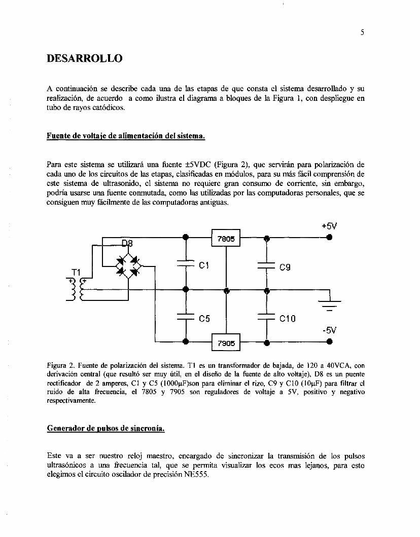
Para este sistema se utilizará una fuente k5VDC (Figura 2), que servirán para polarización de cada uno de los circuitos de las etapas, clasificadas en módulos, para su más fácil comprensión de este sistema de ultrasonido, el sistema no requiere gran consumo de corriente, sin embargo, podría usarse una fuente conmutada, como las utilizadas por las computadoras personales, que se consiguen muy fácilmente de las computadoras antiguas.
Figura 2. Fuente de polarización del sistema. TI es un transformador de bajada, de 120 a 40VCA, con derivación central (que resultó ser muy útil, en el diseño de la fuente de alto voltaje), D8 es un puente rectificador de 2 amperes, C1 y C5 (1OOOpF)son para eliminar el rizo, C9 y C10 (10pF) para filtrar el ruido de alta frecuencia, el 7805 y 7905 son reguladores de voltaje a 5V, positivo y negativo respectivamente.
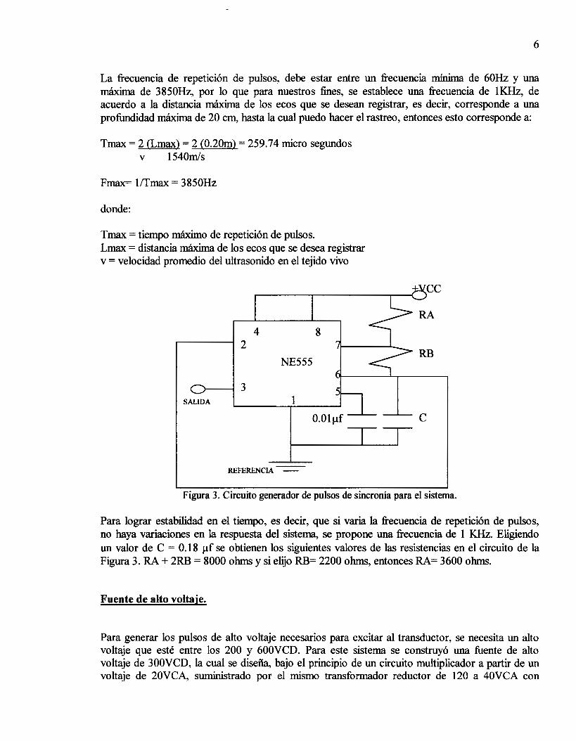
Generador de pulsos de sincronía.
Este va a ser nuestro reloj maestro, encargado de sincronizar la transmisión de los pulsos ultrasónicos a una frecuencia tal, que se permita visualizar los ecos mas lejanos, para esto elegimos el circuito oscilador de precisión NE555.
6
La fiecuencia de repetición de pulsos, debe estar entre un fiecuencia mínima de 60Hz y una máxima de 3850Hz, por lo que para nuestros fines, se establece una fiecuencia de lKHz, de acuerdo a la distancia mhxima de los ecos que se desean registrar, es decir, corresponde a una prohdidad máxima de 20 cm, hasta la cual puedo hacer el rastreo, entonces esto corresponde a:
Tmax = 2 (Lmax) = 2 (0.20m) = 259.74 micro segundos v 1540ds
Fmax= l/Tmax = 3850Hz
donde:
Tmax = tiempo máximo de repetición de pulsos. Lmax = distancia máxima de los ecos que se desea registrar v = velocidad promedio del ultrasonido en el tejido vivo
-I
Figura 3. Circuito generador de pulsos de sincronía para el sistema.
Para lograr estabilidad en el tiempo, es decir, que si varia la fiecuencia de repetición de pulsos, no haya variaciones en la respuesta del sistema, se propone una fkecuencia de 1 KHz. Eligiendo un valor de C = 0.1 8 pf se obtienen los siguientes valores de las resistencias en el circuito de la Figura 3. RA + 2RB = 8000 ohms y si elijo RB= 2200 ohms, entonces RA= 3600 ohms.
Fuente de alto voltaje.
Para generar los pulsos de alto voltaje necesarios para excitar al transductor, se necesita un alto voltaje que esté entre los 200 y 600VCD. Para este sistema se construyó una kente de alto voltaje de 300VCD, la cual se diseña, bajo el principio de un circuito multiplicador a partir de un voltaje de 20VCA, suministrado por el mismo transformador reductor de 120 a 40VCA con

7
derivación central, utilizado por la fuente de polarización, al cual se lleva hasta un valor aproximado de 300VCD.
Algunas otras ideas para generar este alto voltaje, aparentemente mas simples o prácticas, como lo seria por ejemplo, tomar los 120VCA de la línea y duplicarlo, ahorrándonos así el transformador y unas etapas del multiplicador, ó quizá el uso de un transformador elevador a 240VCA, con su etapa de filtrado y rectificado, al intentar con cualquiera de estas dos formas, se encontró que las tierras no se podían acoplar, lo que genera serios problemas, en efecto obteníamos el alto voltaje de forma mas sencilla, pero al conectar el osciloscopio para observar la respuesta ultrasónica, existía una diferencia de potencial entre la tierra fisica de la linea y nuestra referencia en la fuente, 6 si por accidente se conectaba el cable de línea invertido, provocaba un buen corto, por lo que finalmente optamos por el circuito multiplicador, que no presentó este problema, pudiendo mantener una sola referencia para todos los voltajes del sistema y la línea eléctrica. Este circuito multiplicador se muestra en la figura 4, nótese que el voltaje a la salida es en corriente directa, la cual es una característica del circuito multiplicador, debido al arreglo de capacitores y diodos.
c1 c 10 Clr c 12
Dl DS D 12 Dl3 cs c 13
I I
J - referencia "- 300vDc """""""- - +
Figura 4. Fuente de alto voltaje, T1 es el mismo transformador utilizado en la fuente de polarización, de donde se toman 20VCA, el arreglo de capacitores (470pF 63V) y diodos rectificadores (1N4007) en la red multiplicadora, nos da aproximadamente 300VCD.
Disparador de pulsos de alto voltaje.
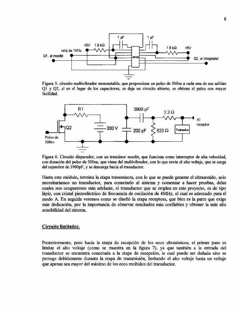
Una vez que se tiene el alto voltaje, este se aplica al transductor, con pulsos de duración menor que la mitad del periodo de la onda ultrasónica, es decir, si el transductor en este caso tiene una fiecuencia de 4MHz, entonces la duración del periodo debe ser menor que 500ns, para esto se emplea un circuito multivibrador monoestable', como se muestra en la figura 5, de tecnología mosfet, que durante este tiempo va a cargar un capacitor, el cual va a ser descargado por medio de un interruptor electrónico (ver figura 6), para el cual se recomienda el uso de un transistor mosfet2 (actualmente, también se consiguen como compuerta de transmisión), debido a su alta velocidad de conmutación y tiempo de recuperación.
' Se recomienda el multivibrador monoestable del fabricante Farchild, MC74HC4538N, ya que experimentalmente encontramos tiene mejor respuesta, para lograr un pulso de 500ns. ' El transistor mosfet, es una buena alternativa, como interruptor de alta velocidad y alto voltaje, aqui utilizamos el MTP4N50 o equivalente.
8
+5V 1.8 kQ 1.8 kQ +5V
reloj de 1 KHz al mosfet e 9 Q2, al integrador
I I I e I
- Figura 5. circuito multivibrador monoestable, que proporciona un pulso de 500ns a cada una de sus salidas Q1 y 42, si en el lugar de los capacitores, se deja un circuito abierto, se obtiene el pulso con mayor facilidad.
R1 Jb ; Al - receptor
300 V
Pulso de 50011s A
T w
- Figura 6. Circuito disparador, con un transistor mosfet, que funciona como interruptor de alta velocidad, con duración del pulso de 500ns, que viene del multivibrador, con lo que envía el alto voltaje, que se carga del capacitor de 3900pF, y se descarga hacia el transductor.
Hasta este módulo, termina la etapa transmisora, con lo que se puede generar el ultrasonido, solo necesitaríamos un transductor, para conectarlo al sistema y comenzar a hacer pruebas, delas cuales nos ocuparemos más adelante, el transductor que se emplea en este proyecto, es de tipo lápiz, con cristal piezoeldctrico de flecuencia de oscilación de 4MHz, el cual es adecuado para el modo A. En seguida veremos como se diseñó la etapa receptora, que bien es la parte que exige más dedicación, por la importancia de observar resultados más confiables y obtener la más alta sensibilidad del sistema.
Circuito limitador.
Posteriormente, pero hacia la etapa de recepción de los ecos ultrasónicos, el primer paso es limitar el alto voltaje (como se muestra en la figura 7) , ya que también a la entrada del transductor se encuentra conectada a la etapa de recepción, la cual puede ser dañada sino se protege debidamente durante la etapa de transmisión, limitando el alto voltaje hasta un voltaje que apenas sea mayor del máximo de los ecos recibidos del transductor.

9
Del circuito Al amplificador de transmisor radiofiecuencia
- - Figura 7 . Circuito limitador, para protección del receptor, principalmente al amplificador de radiofiecuencia, que no soporta un alto voltaje en su entrada.
Ganancia compensada en el tiempo (TGC).
En esta etapa se genera una señal diente de sierra, la cual se utiliza como señal de control, del amplificador de ganancia variable, como parte del modulo de compensación de ganancia en el tiempo, lo que hará que los pulsos que llegan un tiempo después al transductor, se amplifiquen más que los que llegan primero de distancias más cercanas, facilitando de esta manera la visualización de todos las amplitudes en el osciloscopio.
Para la realización de esta etapa se tomará el pulso Q2 del multivibrador, ya que al integrar este pulso se obtiene una rampa que esta sincronizada con la terminación de el pulso de excitación, es decir en cuanto acaba el pulso de 500ns, empieza la rampa, que necesita cada mili segundo, el amplificador de ganancia variable, como señal de control.
t vi
vi
vi pulso de 500ns, cada 1 ms
2.2 nF I I
45 kR ID 4D
m A w
vo
rampa de aproximadamente lms
Figura 8.' TGC, se emplea un circuito integrador; con un OpAm de alta velocidad como se ilustra en b), para obtener la rampa que vemos en c), que se empleara como señal de control del amplificador de ganancia variable. En a) se muestra el pulso que viene de 4 2 del multivibrador, con el fin de no interferir con el pulso Q 1, que controla el interruptor de alta velocidad.
10
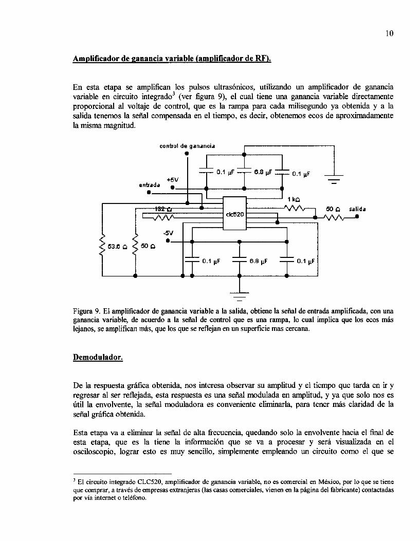
Amplificador de ganancia variable (amplificador de RF).
En esta etapa se amplifican los pulsos ultrasónicos, utilizando un amplificador de ganancia variable en circuito integrado3 (ver figura 9), el cual tiene una ganancia variable directamente proporcional al voltaje de control, que es la rampa para cada milisegundo ya obtenida y a la salida tenemos la señal compensada en el tiempo, es decir, obtenemos ecos de aproximadamente la misma magnitud.
control de ganancia
0.1 pF 6.8 pF 0.1 pF +5v -
entrada - I b
m I d * I kt2
A ' clc520 I
A *
50 n salida
- 1
T I
" " " -- 0.1 pF -- 6.8 pF -- 0.1 pF
1 1 - ..
Figura 9. El amplificador de ganancia variable a la salida, obtiene la señal de entrada amplificada, con una ganancia variable, de acuerdo a la seiIal de control que es una rampa, lo cual implica que los ecos más lejanos, se amplifican más, que los que se reflejan en un superficie mas cercana.
Demodulador.
De la respuesta grhfica obtenida, nos interesa observar su amplitud y el tiempo que tarda en ir y regresar al ser reflejada, esta respuesta es una señal modulada en amplitud, y ya que solo nos es útil la envolvente, la señal moduladora es conveniente eliminarla, para tener más claridad de la señal gráfica obtenida.
Esta etapa va a eliminar la seiial de alta frecuencia, quedando solo la envolvente hacia el final de esta etapa, que es la tiene la información que se va a procesar y será visualizada en el osciloscopio, lograr esto es muy sencillo, simplemente empleando un circuito como el que se
El circuito integrado CLC520, amplificador de ganancia variable, no es comercial en México, por lo que se tiene que comprar, a través de empresas extranjeras (las casas comerciales, vienen en la pigina del fabricante) contactadas por vía internet o teléfono.

11
muestra en la figura 10, que es un demodulador asíncrono, que consta de dos elementos un diodo de rectificación rápida y una resistencia.
Figura 10. Circuito demodulador, en a) ve(t) son los ecos ultrasónicos como se verían antes del demodulador y ya compensados en el tiempo, donde se observa que existe una señal modulada en amplitud y como lo que nos interesa, es solo la amplitud de los ecos ultrasónicos y el tiempo, se utiliza un circuito demodulador como en b) y tinalmente tenemos la señal demodulada vs(t) como en c).
El sistema hasta este momento, ya nos esta proporcionando una información satisfactoria y clara, sin embargo, podría ser conveniente utilizar una última etapa de amplificación, para el caso en que se deseara utilizar un tubo de rayos catódicos y no el osciloscopio, esto es, necesitariamos un amplificador de video, así como un circuito de base de tiempo, que solo se describirán brevemente a continuación.
Amplificador de video.
Para esta etapa se utilizar& un amplificador de voltaje heal4, para lo cual se utilizará el circuito integrado TS272C, amplificador operacional de alta velocidad, tecnología cmos, de uso general, en realidad, esta etapa no es de vital importancia, debido a que la visualización se va a ser sobre la escala vertical del osciloscopio, el cual ya tiene su propio amplificador y se amplifica al variar sobre la escala vertical.
10 k n
srííal d y n r d a 3 1 señal de . salida
Figura 1 l . Circuito amplificador de voltaje de la ultima etapa del sistema.
4 Los amplificadores operacionales utilizados en el sistema, deben de ser de alta velocidad (flash), estos si son comerciales en México, por ejemplo: LF356, TS272C, LM374.
12
RESULTADOS
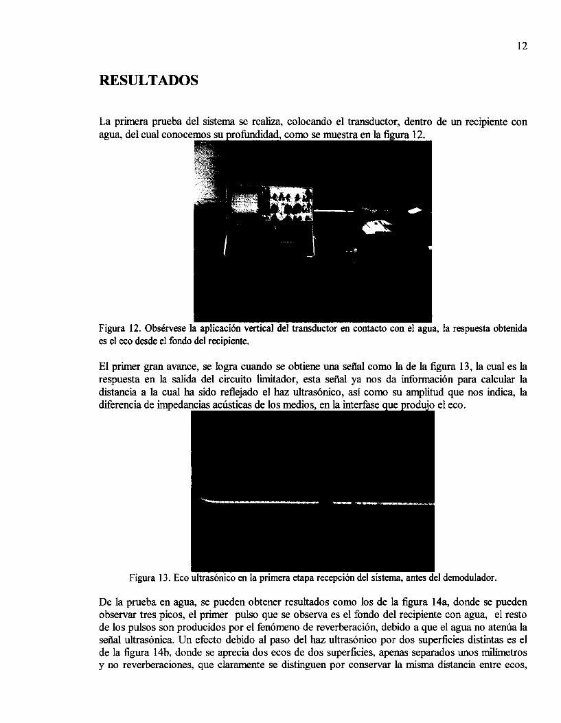
La primera prueba del sistema se realiza, colocando el transductor, dentro agua, del cual conoc
Figura 12. Obsérvese
de un recipiente con
la aplicación vertical del transductor en contacto con el agua, la ob1 t e n i d a es el eco desde el fondo del recipiente.
El primer gran avance, se logra cuando se obtiene una sehl como la de la figura 13, la cual es la respuesta en la salida del circuito limitador, esta seiial ya nos da información para calcular la distancia a la cual ha sido reflejado el haz ultrasónico, así como su amplitud que nos indica, la diferencia de impeda
Figura 13. Eco ultrasónico en la primera etapa recepción del sistema, antes de
el ic
:1 den
:o.
nod lulador.
De la prueba en agua, se pueden obtener resultados como los de la figura 14% donde se pueden observar tres picos, el primer pulso que se observa es el fondo del recipiente con agua, el resto de los pulsos son producidos por el fenómeno de reverberación, debido a que el agua no atenúa la señal ultrasónica. Un efecto debido al paso del haz ultrasónico por dos superficies distintas es el de la figura 14b, donde se aprecia dos ecos de dos superficies, apenas separados unos milímetros y no reverberaciones, que claramente se distinguen por conservar la misma distancia entre ecos,

13
pero atenuados, a diferencia de la otra figura donde el segundo medio, que aunque esta más
a) Figura 14. Ecos ultrasónicos visualizados desde la pantalla del osciloscopio, en a) el haz ultrasónico es dirigido solo hacia un solo medio y en b) se observa la señal de salida del equipo, reflejada en dos superficies, separadas 3 m m dentro del mismo recipiente. Obsérvese, que estas señales son tomadas después de la etapa de amplificación y demodulación.
a) Figura 15. Montaje del sistema en un pequeño chasis de 19 x 15 x lOcm, que contiene la fuente polarización, fuente de alto voltaje (parte más interna) y el resto de las etapas (adelante en la figura b)), así como un pequeño espacio para implementar la etapa para digitalizar la señal, para despliegue en PC (opcional) como se aprecia en b), también en la cubierta posterior se fijan conectores bnc hembras, como salidas parciales en el sistema. En a) se ve el frente y se aprecia una carátula analógica para indicar el alto voltaje, un interruptor general y un conector bnc hembra para el transductor.
14
CONCLUSIONES
El sistema resulta ser muy ilustrativo en su funcionamiento y construcción, con el que finalmente se puede trabajar en docencia.
Otro hecho que resulta ser muy interesante, es que en este sistema trabajamos con alto voltaje en corriente directa y circuitos que requieren alta fkecuencia de operación, contrario a lo que normalmente ocurre con las prácticas de laboratorio, en los cursos de electrónica e instrumentación en ingeniería, experiencia muy valiosa, ya que nos demostró que trabajar con alto voltaje, es muy común en instrumentación médica y el trabajar con alta fkecuencia, nos hace indagar sobre los componentes electrónicos, de más alta tecnología de manufactura.
Se espera que este sea un paso adelante, en el desarrollo de sistemas de ultrasonido más sofisticados, realizados en instituciones educativas y motiven a las autoridades a brindar un apoyo mayor a las áreas de investigación.

15
ANEXO
Hojas de datos del fabricante y especificaciones técnicas de los componentes utilizados para la construcción del presente proyecto.
- Tema Página
Circuito integrado oscilador de precisión NE555 ........................................................................... 16
Circuito multivibrador de alta velocidad M74HC4538 .................................................................. 18
Transistor de potencia, MOSFET canalN, IRF830 ....................................................................... 22
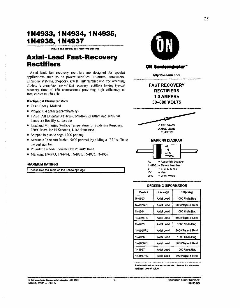
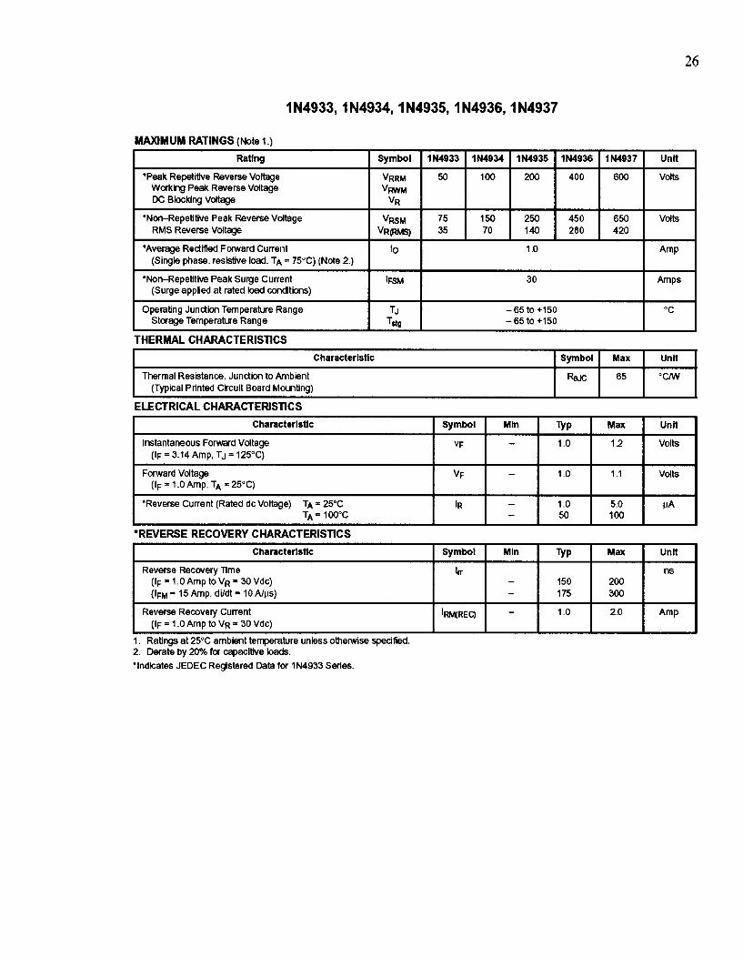
Diodo rectificador de alta velocidad lN4933D .............................................................................. 25
Circuito regulador de voltaje negativo, LM7905 ........................................................................... 27
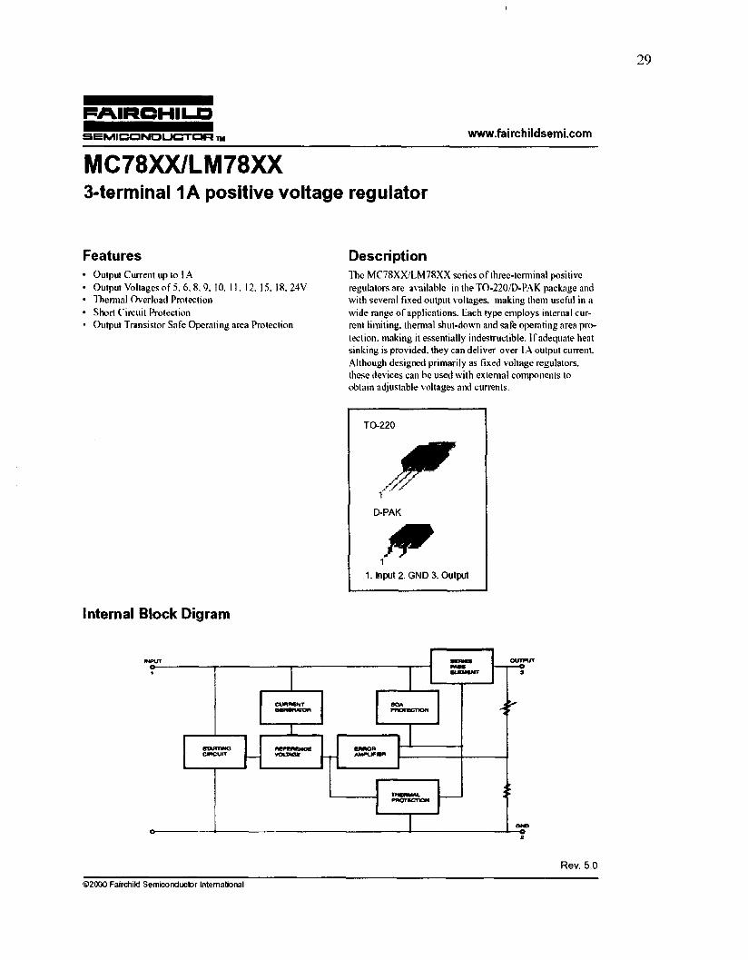
Circuito regulador de voltaje positivo, LM7805 ..................... ....................................................... 29
Circuito integrado amplificador de ganancia variable, CLC520 .................................................... 3 1

16 - FAIRCHILD - -MICOmUCTe3R www.fairchildsemi.com
LM5551NE5551SA555 Single Timer
Features High Current Drive Capztbility (200m.4) - .Adjustable Duty Cycle Temperature Stability of 0.005%/0f Timing From pSec to Hours Turn off Time Less Than 2pSec
Description Thc LM555R\IE555/SA555 is a highly stable controller capable of producing accurate timing pulses. With monostable operation, the time delay is controlled by one external resislor and one capitor. With astable operation, the frequency and duty cycle are accurately controlled with two external lrsistors and one capacitor.
Applications Precision Timing Pulse Generation Time Delay Generation Sequential Timing
I I 41
Internal Block Diagram
"""""' Voltage
Rev. 1 .O2 02002 Fairchild Semicondudor ~ r a l b n

17
Electrical Characteristics (TA = 25°C. Vcc = 5 - IN, unless otherwise specified)
Parameter
vcc Supply Vottage Symbol
I Supply Current "(Low Stable) I k c
Timing Error +2 (Monostable) Initial Accuracy Drift with Temperature Drift with Supply Voltage
ACC U R 4tiAT
AffAVcc
Timing Error *2(Astable) lntial Accuracy
AVAVcc Drift with Supply Voltage Aff AT Drift with Temperature
ACCUR
Control Voltage VC
I Threshold Voltage 1 vTH
I Threshold Current +3 I ITH
I Trigger Voltage 1 VTR
Trigger Current
VRST Reset Voltage ITR
I Reset Current 1 IRST
Low Output Voltage VOL
Fall Time of Output
l lKG Discharge Leakage Current tF
Notes:
Conditions
vcc = 5v, RL = - Vcc = 15V, RL = m
= 1kQ to100kR C = 0.1 pF
R~=1kQto1OOkQ C = 0.1 pF
vcc = 15v vcc = 5v vcc = 1w vcc = 5v
vcc = 5v Vcc = 15V VTR = OV
vcc = 15v ISINK = 1 O m A ISINK = 50mA vcc = 5v ISINK = 5 d vcc = 1w ISOURCE = 200mA ISOURCE = 1OOmA vcc = 5V ISOURCE = 1 O O d
l . Supply current when output is high is typically 1 m A less at VCC = 5V 2. Tested at VCC = 5.0V and VE = 15V 3. This will determine maximum value of RA + RB for 1 5 V operation, the rnax. total R = 2 0 W , and for 5V operation the max.
total R = 6.7MR
18
M54HC4538 M74HC4538
DUAL RETRIGGERABLE MONOSTABLE MULTIVIBRATOR
m HIGH SPEED
m LOW POWER DISSIPATION fpD = 25 ns (TYP.) AT VCC = 5 V
STANDBY STATEICC=~~A(MAX.)ATTA=~~"C ACTIVE STATE kc = 200 pA (TYP.) AT Vcc = 5 V
m HIGH NOISE IMMUNITY VNIH = VNIL = 28 % Vcc (MIN.) OUTPUT DRIVE CAPABILITY 1 o LSTTL LOADS
m BALANCED PROPAGATION DELAYS tpw = ~PHL
m WIDE OUTPUT PULSE WIDTH RANGE tmuT 120 ns - 60 S OVER AT VCC ~ 4 . 5 V
m OUTPUT PULSE WIDTH INDEPENDENT
D PIN AND FUNCTION COMPATIBLE FROM TRIGGER INPUT PULSE WIDTH
WITH 4538B
DESCRIPTION The M54R4HC4538 is a high speed CMOS DUAL MONOSTABLE MULTIVIBRATORfabricatd in sili- con gate C?MOS techndogy. It has the same high speed performance of LSTTL combined with true CMOS low power consumption. Each muftivbrator features both a negative, A, and a positive, 8 , edge triggered input, either of which can be used as an in hibit input. Also included is a clear input that when taken low resets the one shot. The monostable multivibrators areretriggerable. That is,theymay be triggered reapeatedly while their outputs are gem- ating a pulse and the pulse will be extended. Puke width stability over a wide range of t empewe and supply is achievled using linear CMOS techniques. The output pulse equation is simply : PW = 0.7 (R)(C) where PW is in seconds, R in Ohms, and C is in Farads. All inputs are equipped with protection circuits against static discharge and transiat excess volt- age.
B1 R F I R (Plastic Package) (Ceramic Packag?)
M I R C1 R ( M h Package) (Chip Carrier)
ORDER CODES : M54HC4538FlR M74HC4538MlR M74HC453881R M74HC4538ClR
PIN CONNECTIONS (top view)

19
FUNCTIONAL DESCRIPTION (continued)
RESET OPERATION Also transistor Op is turned on and Cx is charged m is normally high. If m is l o w , the trigger is not quickyto VCC. This means i fminpln goes low, the effective because Q output goes low and trgger IC becomes waiting state both in operating and non control flip-flop is reset. operatirg state.
TRUTH TABLE
INPUT AND OUTPUT EQUIVALENT CIRCUIT I
OWWl
PIN DESCRIPTION IEC LOGIC SYMBOL
PIN No NAME AND FUNCTION SYMBOL 1, 15
I CD, 2C D 3, 13
External ResistorKapacibr 1T2,2T2 2, 14
External Capacita IT1 ~ 2T1
Direct Reset Inputs (Active LOW)
CoMlectiMls
Connections " - 1 4,: :: I 1 4 2A I Triggerlnplts (LOWto 1
HIGH, Edge-Triggered) I:, 2E Trigger lnwts (HIGH to
LOW, Edge-Triggered)
u 2E 2 s nt n2

20
DC SPECIFICATIONS
RECOMMENDED OPERATING CONDITIONS

21
MMIM74HC4538
AC ELECTRICAL CHARACTERISTICS (CL = 50 pF, Input tr = tf = 6 ns)

22
July 1998
/RF8305 /RF83I, /RF83Z5 /RF833
4.0A and 4SA, 450V and SOOV, 1.5 and 2.0 Ohm, N-Channel Power MOSFETs
Features 4.0A and 4 . s 450V and 500V
~DS(ON) = 1 .M and 2.OR
Single Pulse Avalanche Energy Rated
SOA is Power Dissipation Limited
Nanosecond Switching Speeds
Linear Transfer Characteristics
High Input Impedance
Related Literature - TB334 “Guidelines for Soldering Surface Mwnt
Components to PC Boards”
Ordering Information
PART NUMBER BRAND PACKAGE I
IRFWO
IRF832 TO-22OAB RF032
IRF831 TO-22OAB RF831
IRF830 TO-22OAB
NOT‘E: When ordering. include the mtie part number.
IRF833 T0-22OAB RF833
Description These are N-Channel enhamment mode silicon gate pawer 6 M effect transistors. They are advanced power MOSFETs d e s i g n e d , ksted, and guaranteed to withstand a specifed level of energy in the breakdown avalanche mode of operation. All of these p o w MOSFETs are designed for applications such as switching regulators. switching m n v e r b r s , motor drivers, rday drivers, and drivers for high power bipolar witching transistors requiing high speed and l o w gate drive power. These types on be operated dredly from integrated circuits.
Formerly developmental type TA17415.
Symbol t o
G @
Packaging JEDEC TO-220AB
File Number 1582.2
23
IRF830, IRF831, IRF832, IRF833
Absolute Maximum Ratings T~ = 25%. Unl~O~henrviseSpecified
Drain b Source W m (Nobe 1) .................... .VDS 500 450 500 450 V
Continuous Dram Current.. . . . . . . . . . . . . . . . . . . . . . . . . . . .ID 4.5 4.5 4 .O 4 .O A Tc lO@C. . . . . . . . . . . . . . . . . . . . . . . . . . . . . . . . . . . . . .ID 3.0 3.0 2.5 2.5 A
Pulsed Drain CUITMI~ (N 3) ....................... ID M 18 18 16 16 A Gate to Source Wtage. . . . . . . . . . . . . . . . . . . . . . . . . . . . . VGS QO G O 320 *20 V
Linear Derating Facta . . . . . . . . . . . . . . . . . . . . . . . . . . . . . . . . 0.6 0.6 O .6 0.6 WPC Single Pulse Avalémdm Energy Rating (N& 4) . . . . . . . . . EAs 300 300 300 300 mJ Operating and StorageTempxabxe . . . . . . . . . . . . . TJ.TS= 6 5 b 1 5 0 -55to150 -55b 150 -56 b 150 “C Mzcd~n~rn Tanperalum for Soldering
Leadsat 0.063im (1.6mm) konr Case br 10s. . . . . . . . . . . TL 300 300 300 300 oc Padcage Body for los, Soe Bchbriof 334 . . . . . . . . . . . .Tpb 260 260 280 m oc
IRF830 IRF831 IRFE32 IRF833 UNITS
Drain b Gate Wage (RGS = 2okn) (N& 1) . . . . . . . . . V ~ R 500 450 500 450 V
b b h n l &@h. ......................... PD 75 75 75 75 W
d h e ~ e f h s a a a r a n y d h a r ~ s ~ l h o s s ~ h h e ~ s e d i o n o d h i s s ~ i o M ( ~ .
N O T E :
C A ~ ~ : S b e o s s s a b o c s ~ B l e d m ~ ” A b w M B R e ~ ’ m a y c a u r r e ~ ~ ~ I b L h s ~ . 7 h i s i s a s ~ ~ ~ e n d ~
1. TJ = 25OC b l e c .
Electrical Specifications Tc = Z0C, UntessOthemiseSpecified
I PARAMETER I SYMBOL I TEST CONDITIONS
Drain to Source Breakdown Voltage BVms V e = OV, ID = 25OpA (Figure 10)
ZeroGate Voltage Drain Current VDS BVDSS, VGS ov IDSS
VDS = 0.8 X Raled BVms. V a = o\r, TJ = 1 2 f l
On-State Drain Current (Note 2) VDS ’ I D ( C N ) x OS(ON)MAX. VGS = 1 I D ( 0 N ) IRF830, IRF831
IRF832. IRF833
Gab to Source Leakage
V e = 1W. ID = 2.5A(Figures 8.9) ~ S ( O N ) Drain bSource On Resistance (Note 2)
v e = G W k=,ss
IRF830. IRFWI
IRF832. IRF833
Fonvard Transmductance (Note 2) VDS > 1ov. ID= 2.7A(F¡UP@ 12)
Tum-On Delay Time VDD = 2 5 w , ID 4.W. RG = lm, RL =54R
Rise Time Essentially lndependen t of Operating
Tumaff Delay Timo
Fall Time
(Figures 17.18). MOSFET Switching Times am
Temperature.
Total Gab Charge VGS = lOV, ID z 4.54 VDS = 0.8 x R&d BVDS! I~REF) = 1.5mA (Fgures 14.19.20) Gatecharge is Essenlialty
Gate to Source Charge Independent of Operating Temperature.
. - 15 n ns
- 33 53 ns
- 16 23 ns
- 22 32 nC
- 3.5 - nC
- 11 - nC
24
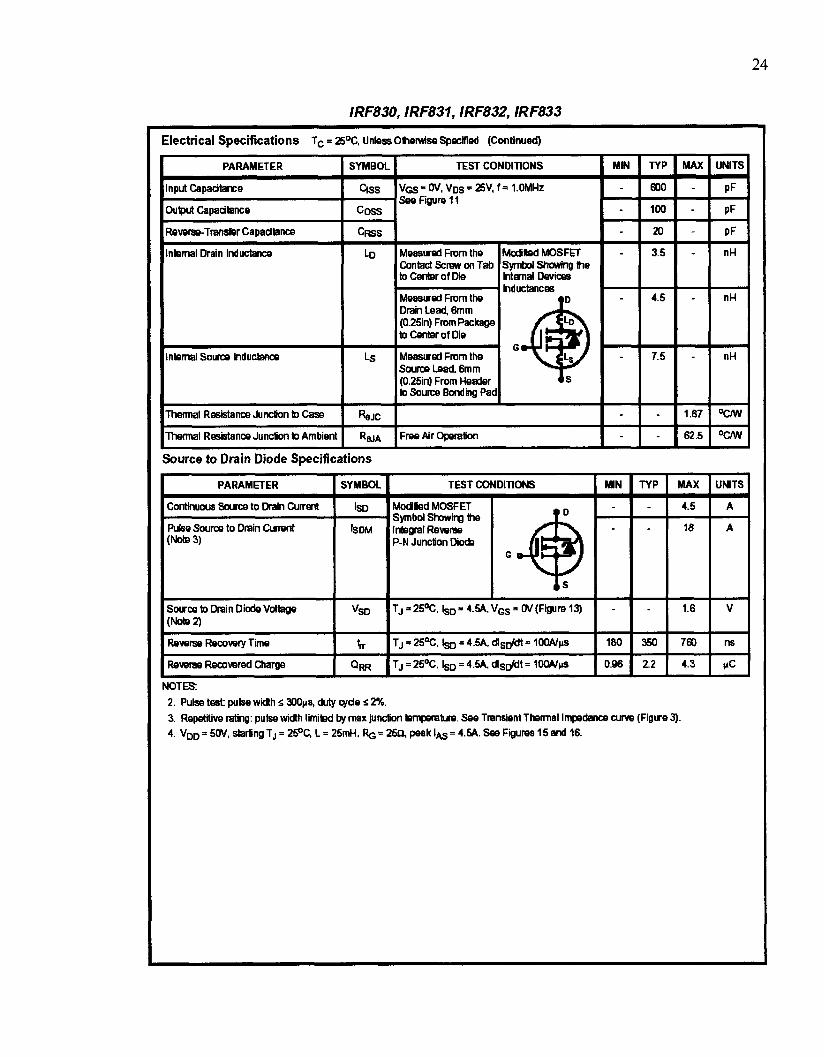
Electrical Specifications Tc = EoC, Unless Olhomiso Specified (Continued)
I PARAMETER I SYMBOL I TEST CONDITIONS
Input Capacitance
Ou$ul C a p a d b e
V a = W, VDS = Z V , f = 1.OMHz
CRSS Reverse-Transfer CaDadWm
coss See Figure 11
l lnbmal Drain Inductance Measured F m the Modifad MOSFET Contad Screw on Tab I Svrnbol Showina U?e to Cerbr of Die
Measured From tho Drain Lead, 6mm (0.25in) F m Package to Cenler of Die
Inbemat Source inductance Measured Fmrn the L.s
to Source Bonding Pac @.25m) From Header Soum Lead, 6mm
ThennalResistanceJundiontoCas 5 J C
G @ Thenal Resstance Junction to Ambient
Source to Drain Diode Specifications
I PARAMETER I SYMBOL
Reverse Recovefy Time h Reverse Recovered Charge QRR
TEST CONDITIONS I Y N
Modl[ed MOSFET Symbol Shwrirg the
P-N Junction Dioda G
- 4.5
- 7.5
- 1.67
62 5 -
NOTES: 2. Pulse tsst: pulsa width g 300ps, duty qde 2%. 3. Repetitive rating: pulse width limitad by rnax junction bamperabre. See Transient Themal Impedance cum (Figure 3). 4. VD, = 5W, starling TJ = 2PC, L = 25mH. RG = 2!X& peak Im = 4.M. See Figures 15 and 16.
MAX
4.5
UNITS
A 18
A
1.6 V
760
pc 4.3
m
25
I N4933, I N4934, I N4935, I N4936,l N4937
IN4935 and IN4937 are Preferred Devices
Axial-Lead Fast-Recovery Rectifiers
Axial-lead. fast-recovery rectifiers are designed for special applications such as dc power supplies, inverters. converters, ultnsonic systems, choppers, low RF interference and free wheeling diodes. A complete line of fast recovery rectifiers having typical recovery time o f I50 nanoseconds providing high efficiency al frequencies to 250 kHz.
Mechanical Characteristics Case: Epoxy, Mottled Weight: 0.4 gntn (approximately) Finish: A11 Extenial Surfaces Corrosion Resistant and Tenninal
Lead and Moimting Surface l'empenhw.? for Soldering I'uqmses:
Shipped in plaslic bags. I O00 per bag. Available ' l a p and Reeled. 5000 per reel. by adding a "KL" suffix lo
Polarity: Cathode Indicated by Polarity Band Marking: IN49.3. 1N4934. IN4935. IN49-36. IN1937
Leads are Readily Solderable
220°C Max. for IO Seconds, 1 / 1 6 " from case
the part nuniber
MAXIMUM RATINGS I Please See the Table on !he Followina Pme I
W"" httpY/onsemi.com
FAST RECOVERY RECTIFIERS 1 .O AMPERE
50-600 VOLTS
CASE 59-03 AXIAL LEAD
pusnc
MARKING M A G W
4 9 3
AL = Assembly Location 1 N493x - Device ,Wmber x - 3. 4. 5 . 6 or 7 W -Year WW =Workweek
ORDERING INFORMATION
1 N4933
1 N4934 Axial Lead
1N4934RL Axial Lead
1N4935
1N4936RL
Axid Lead 1 N4936
Axial Lead lN4935RL
Axial Lead
Axial Lead 1N4937RL
Axial Lead 1 N4937
Axial Lead
1 0 0 0 unitmag
50001Tape 8 Reel ~~ ~
1000 UnitsBag
50001Tape 8 Reel
1 o00 UnitsEag
5000/Té@e 8 Reel
l o 0 0 Units-
1 SOOOITape 8 Reel
Q s r m i c m d u d o r ~ b hb.tr*.. LLC. M 0 1 I m
PuMication Order Number: March, 2001 -Rev. 5 1 N4933/D
IpMs*Iprs
26
1N4933, I N4934,1N4935,1N4936, IN4937
MAXIMUM RATINGS (Note 1 .)
Rating
Vdts 600 400 200 100 50 VRRM "Peak Repetitive Reverse Voltage
Unit 1N4937 1N4936 IN4935 IN4934 IN4933 Symbol
Workhg Peak Rwerse Voltage DC Blocking Voltége
VWM VR
"Non-Repetitive Peak Reverse Voltage Volts 650 45 O 250 150 75 VRSM RMS Reverse Voltage 420 280 140 70 35 VRIRMS)
I I I
"Average R e d M Fonnrard Current Amp 1 .o lo (Single phase. resistive load, TA = 75°C) (Note 2.)
'Non-Repetitive Peak Surge Current 30 ~FSM (Surge applied at rated load conc8tions)
Operating Jundion Temperature Range "C - 65 to +I50 TJ Starage Temperature Range - 65 to +150 Tag
THERMAL CHARACTERISTICS
I Characteristic I Symbol I Max I Unit
Thermal Resistance. Jundion to Ambient I (TvDical Printed Circuit Board Mwit inal "CNU
ELECTRICAL CHARACTERISTICS Characteristic
Volts 1.2 1 .o - VF Instantaneous Forward Voltage
Unit Max VP Min Symbol
(IF = 3.14 Amp, TJ = 125°C)
Forward Voltage Vdts 1 .I 1 .o - VF (IF = 1 .O Amp. TA = 25°C)
*Reverse Current (Rated dc Voltage) TA = 25°C PA 5.0 1 .o - IR TA 100°C 100 50 -
'REVERSE RECOVERY CHARACTERISTICS Characteristic
ns tfT Reverse Recovery Time
Unit Max VP Min Symbol
( I F = 1 .O Amp to VR = 30 Vdc) ( I ~ ~ = l 5 A m p , d i l d t = l O A / l l s )
200 150 - 300 1 75 -
Reverse Recovery Current Amp 2.0 1 .o - IWREC) (IF = 1 .O Amp to VR = 30 Vdc)
1. Ratings at 25°C ambient temperature unless otherwise specifled. 2. Derate by 20% for capacitive loads. 'Indicates JEDEC Registered Data for IN4933 Series.

27
N a t i o n a l S e m i c o n d u c t o r
I LM79XX Series 3-Terminal Negative Regulators
General Description The LM79xX series of %terminal reguletors is availaMe with
These devices need onfy one external compo"-e com- pensation capacitor at me output. me LM79xX series is packaged in the T0-220 pawer package and is capable of supplying 1.5A of output cucrent. These regulators employ internal current limitby safe area protection and thermal shuMown f o r protection against v'r- tually all overbad conditions.
vdage to be eesly boosted above me preset value with a resistor divider. The l a w quiescent current drain of
fixed Output vol- of -5V. -8V, -12V. and -15V.
Law ground pin alnent of me LM79xx series alorws outpld
Connection Diagrams Te220 Pscleg. bz
GROUND
N W f 7 3 d O - (1
FrontVkw
Older Number UnSasCr, LM791ZCT or u17915CT Sea NS padcsp Number TOae
these devices w&h a specified maximum change with I h e and l o a d ensures good reguWon in the vol- boosted moda For applications requihg other voltages, see LM137 data sheet
Features m T h e m r a l , short cicuit and safe ama protection
High rime rejection
m 4% tolerance on preW oytput voltaga 8 l.!% OUtpld Cund
Typical Applications
4 7 . ; Fbrd Roguhtor
2.234
INnJT LYPOXXCI OUlP01
wnmd~-3 *Required I mgllator is separated from Hter capacitor by more than 3". For value giu- capacitor must be adid tantalum 25 pF aluminum electrolytic may be substituted.
tR-ed for stability. For value g i v a n , capacbr must be solid tantalum. 25 pF aluminum electrolytic may be substi- Med. Values giuen may be maeased without hit For output capacitance in excess of 100 pF, a high w r r d dbde f r o m input to output (1 N4001, etc.) d l protect me mgllator from momentary input shorts.

28
29
www.fairchildsemi.com
MC78XXILM78XX %terminal 1A positive voltage regulator
Features Description Output Current up to I A I l le MC78XNLM78XX series of three-temlinal positive Output Voltages o f 5.6.8.9. IO. 1 I . 12. 15. 18. 24 ' regulators are available i n theT0-220,Q-P.AK pachlge and Ihernlal Overload Pmtection with several fixed output voltages making them usefill i n a Short Circuit Protection wide mnge of applications. Each type employs internal cur-
* Output Transistor Safe Operating area Protection rent limiting. thernlal shut-down and safe olxrating area pro- tection. making it essentially indesinctible. I f adequate heat sinking is provided. they can deliver over IA output current. Although designed prilnarily as fixed voltage regulators. these devices can be used with extemal components to obtain adjustable voltages and currents.
I TO-220
1. Input 2. GND 3. Output
Internal Block Digrarn
Rev. 5.0
92000 Fairchild Semiconducbr International

30
MC78XXIlM78XX
Absolute Maximum Ratings I Parameter I Symbol I Value I Unit 1
Input Voltage (for Vo = 5V to 18V) V 35 VI (for Vo = 24V) VI
OC O - +I25 TOPR Operating Temperature Range (MC78XXCTILM78XXCTIMC78XXCDT)
O C M l 65 R0JA Thermal Resistance Junction-Air
OCNV 5 R e ~ c Thermal Resistance Junction-Cases
V 40
I Storage Temperature Range I TSTG I -65 - +I50 I O C I
Electrical Characteristics (MC78051LM7805) (Refer to test circuit .PC < TJ < 125OC. Io = 500mA. VI = IOV. CI= 0.33~1:. CO= O. lpE unless otherwise specified)
MC780YLM7805 Min. I TYP. I Max.
Parameter Conditions Symbol m Unit
TJ =+25 OC
VI = 8V to 20V
5 . 0 ~ 4 lo < 1 .OA, P o 15W 5.2 5.0 4.8
Output Voltage vo VI = 7V to 20v 4.75
4.0 vo = N to 25v
5.25 5.0
50 1.6 VI = 8V to 12V 100
V
Line Regulation T~=+25 O C AVO mV
lo = 5.0mA tol.5A
50 4 750mA
100 9 - Load Regulation
Quiescent Current
rnV lo =250rnA to TJ=+25 AVO
rnA 8 5.0 TJ =+25 OC I Q
Quiescent Current Change lo = 5rnA to 1 .OA
1.3 0.3 0.5 0.03 -
'IQ VI= 7V to 25V mA
Output Voltage Drift
w 42 f = 10Hz to IOOKHz, TA=+25'C VN Output Noise Voltage
mVl°C - -0.8 - lo= 5mA AVOIAT
Ripple Rejection I RR I f = 120Hz Vo = 8V to 18V
Dropout Voltage
A - 2.2 TJ =+25 OC IPK Peak Current
rnA - 230 - VI = 35V, TA =+25 O C ISC Short Circuit Current
mR 15 f = 1KHz R o Output Resistance
V 2 lo = IA, TJ =+25OC vo
Load and line regulation are specified at constant junction temperature. Changes in VO due to heating effects must be taken into account separately. Pulse testing with low duty is used.
National Semiconductor
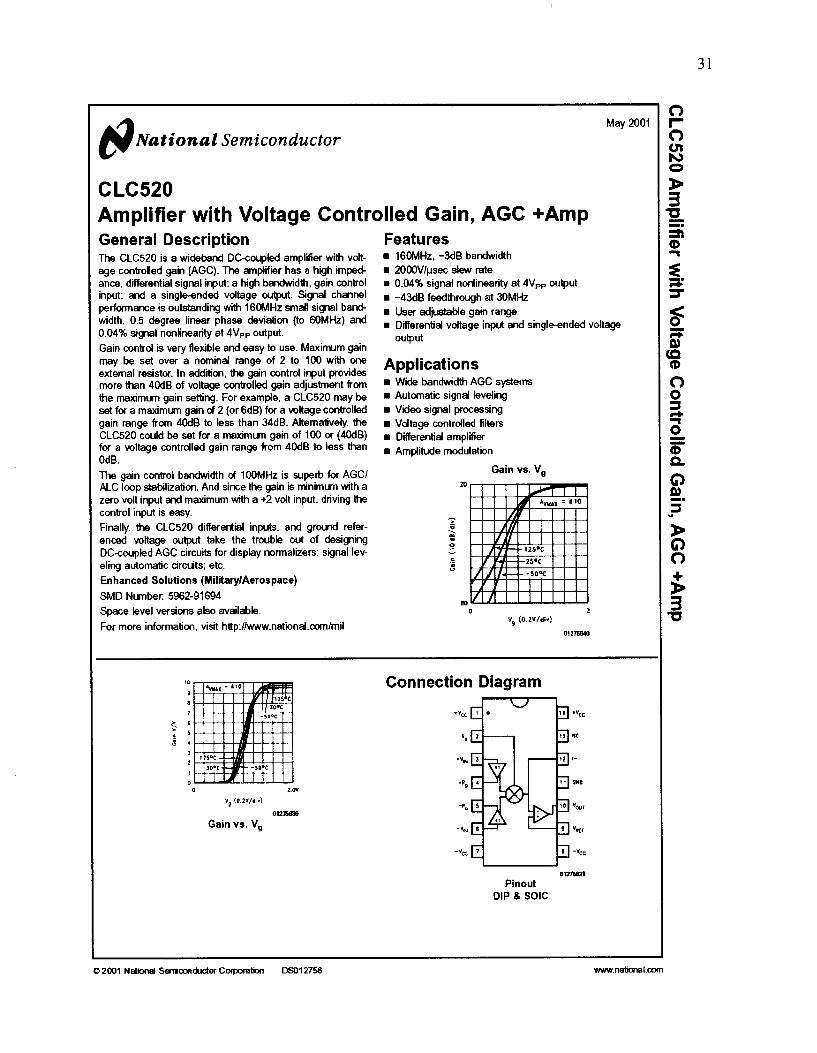
CLC520 Amplifier with Voltage Controlled Gain, AGC +Amp General Description The CLC520 is a wideband DCcoupled amplifier with volt- age controlled gain (AGC). The mpllier has a hgh imped- ance, differential signal input: a high bandwidth, gain control hput; and a single-ended voltage output. S i p 1 channel performance is outstanding with 16ob+k smdl s i p 1 band- width. 0.5 degree linear phase deviation (to GOMHz) and 0.04% s i p 1 nonfinearity at 4Vpp output. Gain contrd is very flexible and easy to use. Maximum gain may be set over a nominal range of 2 to 100 with one extenml resistor. In addition. the gain contrd input provides more than 4OdB of v o l t a g e controlled gain adjustment from the maximum gain setting. For example, a CLC520 may be set for a maximum gain d 2 (or 6dB) for a wltage controlled gain range from 4OdB to less than 34dB. Alternatively. the CLC520 could be set for a maxirnun gain of 100 or (4OdB) for a voltage contrdled gain range from 4OdB to less than OdB. The gain control bandwidth d l00MHz is superb for AGCl ALC loop stabilization. And since the gain is mininum with a zero vdt input and maximum with a +2 vdt input. driving the control input is easy. Finally. the CLC520 differential inputs. and ground refer- enced voltage output take the trouble out of designing DC-cwpled AGC circuits for display normalizers: signal lev- eling automatic a r c h ; etc. Enhanced Solutions (MilitatylAerospace) SMD Nunber. 5962-91694 Space level versions also available. For more information. visit http:/hrvww.national.comhnil
May 2001
Features
m 2000V/psec slew rate m 160" , -3dB bandwidth
m 0.04% signal nonlinearity at 4V, output m -43dB feedthrough at 30MHz m User adplstable gain range m Differentid voltage i n m and singleended voltage
output
Applications m Wide bandwidth AGC systems m Automatic signd leveling m Video signal processing m Vdtage contrded filters m Differentid amplifier m Amplitude modulation
Gain vs. Ve
IO
S
8 7
6
5 . S
2 I
O O
Yg I0.2rld I1
Gain vs. Ve
1.w
01216gY)
Connection Diagram
0121682)
Pinout DIP 8 SOlC
6omA fV,
1 ov fV,
fVcc
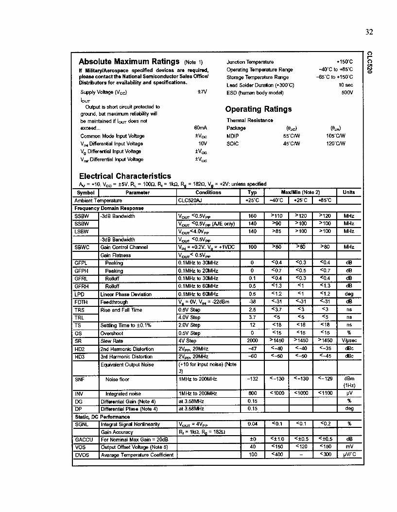
Absolute Maximum Ratings (Note I) Junction Temperature +150C If Militav/Aerospace specified devices are required, Operating Temperature Range -4o'C to 45°C please contact the National Semiconductor Sales Office/ Storage Temperature Range -65'C to +150C Distributors for availability and specifications. Lead Solder Duration (+3OOC) 10 sec supply Voltase VCC) f7v ESD (human body model) 500V IOllT
Output is short circuit protected to grwxl , but maximum reliability w i l l be maintained if low does not Thermal Resistance exceed ... Package @ J 3 @ J J
Common Mode Input Voltage MDIP 5 5 a W 105'CIW V,, Differential Input Voltage SOlC 4 5 c M I 120" V, Differential Input Voltage V, Differential Input Voltage
Operating Ratings
Electrical Characteristics A,, = +lo, Vc, = f5V. R, = lOOn, R, = I&, Q = 1824 Va = +2V; unless spe&ed
Symbol I Parameter Conditions I TYP I M a x " (Note 2) I Units Ambient Temperature I CLC52opJ I +25'C I -4O'C I +25C I 45°C I Frequency Domain Response
Static, DC Performance SGNL lntegal Signal Nonlinearity v,, = 4VPP 0.04 cO.1 '0.1 <0.2 %
GACCU For Nominal Max Gain = 20dB fO <+1.0 Cf0.5 <+OS dB VOS Output Offset Voltage (Note 5) 40 <150 <I20 '150 mV
DVOS Average Temperature Coefficient 100 '400 - '300 pVI'C
Gain Accuracy Rf= I&, Rg= 1 8 m
32
P 8 h) O

33
Electrical Characteristics (Continued)

34
Application Information
1 2 p O l l m a R
FIGURE 1 . CLC520 Simplified Schematic
Simplified Circuit Description A simplied schematic for the CLC520 is given in figure 1. +VI, and -VI, are buffered with dosed-loop voltage follow- ers inducing a signal current in R, proportional to (+VIN)-(-VIN), the differential input voltage. This curent con- trols a current source which sq>plies two we# matched tran- sistors, Q l and Q2. The current flowing through Q2 is converted to the final output voltage using R, and output amplifier, U1. By chang- ing the fraction of the signal curent I whih flows through Q2 the gain is chsnged. This is done by changing the voltage applied differentially to the bases of Q1 and Q2. For ex- ample, with Ve = O, Q1 is on and Q2 is off. With zero signal current of flowing through Q2 into R,. the CLC520 is set to minimum gain. Conversely, with Ve = 2V, Q1 is off and all of the signal current I flows through Q2 to R, producing maxi- mum gain. With Ve set to 1.1V. the bases of Q1 and Q2 are set to approximately the same voltage, causing ther collec- tor currents to equally divide the signal current I , and estab- lish the gain at one half Ute maximm gain. Typical application circuit figure 2 illustrates a voltagecontrolled gain bbck offering broadband performance in a 5On system envirorment. The input signd is applied to Pin 3 of the CLC520 and terminating resistor R2. Gain contrd signals are applied to pin 2. The net gain control port input impedance is SOR, set by the parallel combination of R1 and the 75oR input impedance of pin 2 of the CLC520. R, is set to the standard value, lko, and & sets the maximum voltage gain to 1OVN. Output impedance is set by R, to 5On so with Son sowce and load termina- tions. the gain is approximately 14dB.
FIGURE 2. CLCS20 Typical Application Circuit
Capacitors Cl-C6 provide broadband power supply bypass- ing. C2 and C5 should be tantalum capacitors. All other capacitors should be high quality ceramic capacitors (CK-05 or equivalent). Adjusting offset offset can be broken into two parts; an input-referred term and an output-referred term. The input-referred offset shows up as a variation in output voltage as V, is changed. This can be trimmed using the c ia i t in fgure 3 by placing a low frequency square wave (V,, = O to 2V, into V, with VI, = OV, the input referred V, term shaws up as a small square wave riding a DC value. Adjust R, to null the V, square wave term to zero. After adjusting the input-referred offset, adjust R2 (with VF( = O, V, = O) until VWT is zero. Finally. for inverting applications VI, may be applied to pin 6 and the offset adjustment to pin 3. This offset trim does n o t improve output offset temperature coefficient.
FIGURE 3. CLC520 Offset Adjustment Circuitly (other external elements not shown)
Selecting component values Most applications of the CLC520 adjust the gain to maximize the V,, s i p l . When referred back to the input, this means
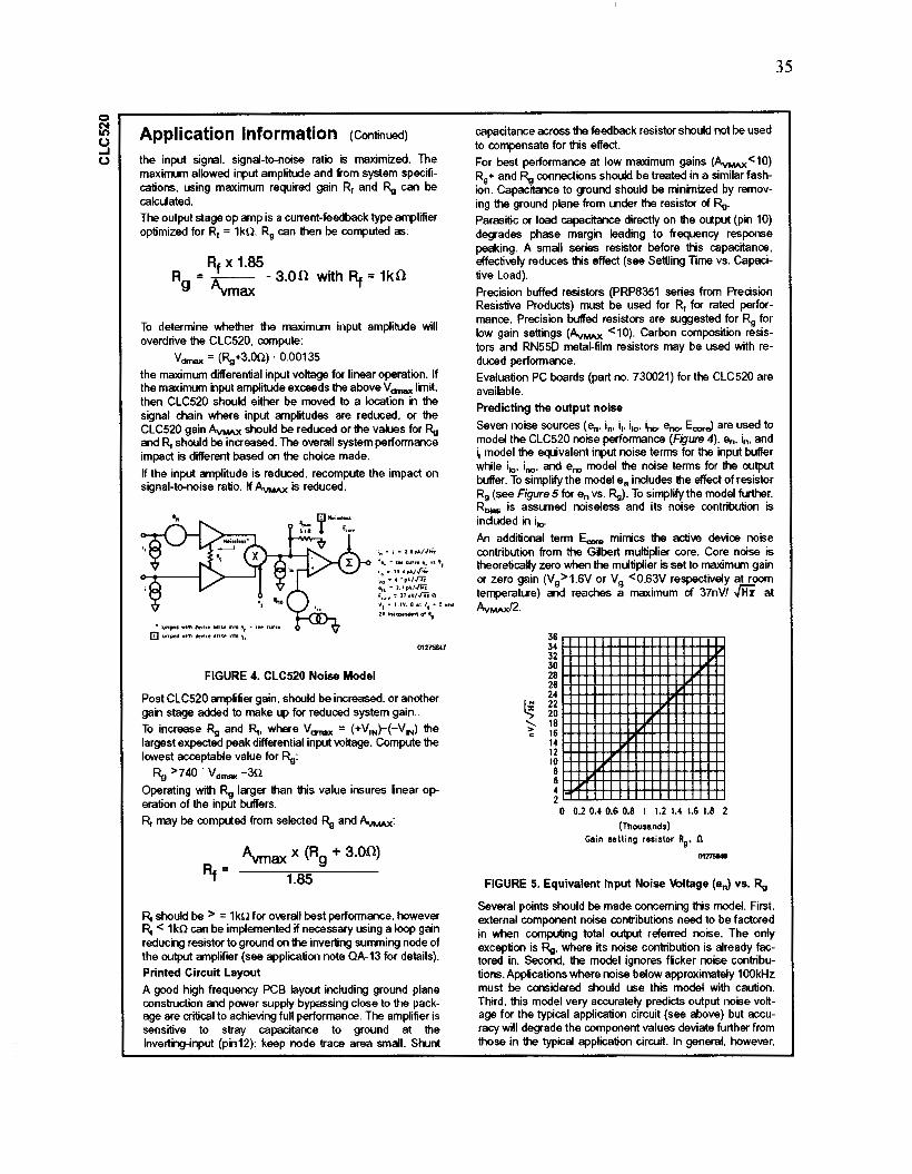
35
Application Information (continued)
the input signal. sgnd-to-noise ratio is maximized. The maximum allowed input amplitude and from system specifi- cations, using maximum required gain R, and R, can be &dated. The output stage op amp is a current-feedback type amplifier optimized for R, = 1kQ. R, can then be computed as:
q x 1.85
g %max R = - - 3.0n With 9 = 1kQ
To determine whether the maximum input amplitude will overdrive the CLC520, compute:
the maximum differential input voltage for linear operation. If the maximum input amplitude exceeds the above V,, limit. then CLC520 should either be moved to a location in the signal chain where input amplitudes are reduced, or the CLC520 gain A- should be reduced or the values for and R, should be inaeased. The overall system performance impact is different based on the choice made. If the input amplitude is reduced. recompute the impact on signal-to-noise ratio. If Av" Is reduced,
V,, = (%+3.oiL) . 0.00135
0127E&7
FIGURE 4. CLC520 Noise Model
Post CLC520 ampbfier gain, should be increased. or another gam stage added to make up for reduced system gain.. To increase R, and R,, where VmX = (+VIN)-(-Vw) the largest expected peak differential input voltage. Compute the lowest acceptable value for $:
Operating with R, larger than this value insures linear o p eration of the input buffers. R, may be complrted from selected R, and b:
R&! '740 " v,, -a
R( should be > = 1 kR for overdl best performance. however R, < 1kR can be implemented if necessary using a loop gain reducing resistor to ground on the inverting summing node of the output amplifer (see application note QA-13 for details). Printed Circuit Layout A good hgh frequency PCB layout including ground plane construction and paver supply bypassing close to the pack- age are critical to achieving full performance. The amplifier is sensitive to stray capacitance to ground at the Invertinginput (pin12); keep node trace area smdl. Shunt
capacitance across the feedback resistor should not be used to compensate for this effect. For best performance at low maximum gains (&<lo) Rg+ and & connections should be treated in a similar fash- ion. Capacitance to gound should be mininized by remov- ing the ground plane from under the resistor of %. Parasitic or load capachce directly on the output (pin IO) degrades phase margin leading to frequency response w i n g . A smdl series resistor before this capacitance. effectively reduces this effect (see Settling Time vs. Capaci- tive Load). Precision buffed resistors (PRP8351 series from Precision Resistive Products) must be used for R, for rated perfor- mance. Precision buffed resistors are suggested for R, for low gain settings (AvMLIx <lo). Carbon composition resis- tors and RN55D metal-film resistors may be used with re- duced performance. Evaluation PC boards (part no. 730021) for the CLC520 are available. Predicting the output noise Seven noise sources (e,,. in. i,. i,. e,, E-3 are used to model the CLC520 noise performance (Figwe 4). e,. in, and i model the equivalent input noise terms for the input buffer while ilo, ino. and e, model the noise terms for the output buffer. To simplify the model e, includes the effect of resistor R, (see Figure 5 for e, vs. Rg). To simplify the model Mher, R,, is assumed noiseless and its noise contribution is induded in i,. An additional term E, mimics the active device noise contribution from the Glbert multiplier core. Core noise is theoretically zero when the multiplier is set to maximum gain or zero gain (Vg>1.6V or V, e0.63V respectively at r m temperatwe) and reaches a maximum of 37n~1 X at AVMAXQ.
36 u 32 30 28
24 26
22 20 18 16 I4 12 10 8 6 4 2
O 0.2 0.4 0.6 0.8 1 1.2 1.4 1.6 1.8 2 (Thousands)
Gain setling resistor Rg. I-¿
"
FIGURE 5. Equivalent Input Noise Wtage (en) vs. % Several points should be made concerning this del. First, external component noise contributions need to be factored in when computing total output referred noise. The only exception is F+,, where its noise contribution is already fac- tored in. Second, the model ignores flicker noise contribu- tions. Applications where noise below approximately lOOkHz must be considered should use this model with caution. Third. this model very accurately predicts output noise vok- age for the typical application circuit (see above) but accu- racy w i l l degade the component values deviate further from those in the typical application circuit. In general, however.
" .

Application Information (continued)
the model s h a d predict the equivalent output noise above the flicker noise region to within a few dB of a d d perfor- mance over the normal range of A,,,.,Ax and component values.
.*^ ."""""_.
E: = ( i b . l k Q 2 + aT(1 kR) + [e, (1 + 5kn )I2 lkfl
C, does not amtribute to the output buffer noise because the output buffer non-inverting input is gwnded. The core noise is already output referred and is 37nVI .& atVg=l . l (A-E!)andapproad-teszeroasAgoestoOor A,, Summing the noise power for each term gves the total output noise pcwer. The total output noise voltage is given by:
01216110
FIGURE 6. Typical Circuit
m m 1 1
FIGURE 7. Noise Model for Typical Circuit
Calculating CLC520 output noise in a typical circuit To cdculate the noise in a CLC520 application, the noise terms given for the amplifer as well as the noise term of the external components must be included. To clarrfy the tech- r i p s used, output noise in a typical circuit will be calcu- lated. (Figure 6) The noise model is depicted in Figure 7. The diagran as- sumes spot noise source with Vr,/& and Amps,,,,$ & wits. The Thevenin equivalent of the source and input ter- mination is used; 25Q in series with a noise voltage source. F$ is assumed noiseless since its effect is included in e,. The internal 5kzz resistor at the CLC520 core output is also assumed noiseless since its effect is included in i,, The noise contribution from Rr is modeled as a noise source. The easiest way to analyze the output noise of this cicuit is to divide the noise paver into three p i e c e s ; -input buffer noise calculation. output buffer noise and core noise. The input buffer varies with the gain. The output buffer term is constant. The core noise term is zero at both maximum and minimum gain and reaches peak at Av,.&2. Since we assume all noise terms are uncorrelated, the equivalent input noise voltage -red is given by:
E: = MTB + ( 1 p 2 + e:
i, does not contribute to the output buffer noise because the input buffer inverting input is grounded. e, is taken from Figure 5. The equivalent output buffer noise is given by:
Where A,, is the input to output voltage gain, which varies with Ve. C accounts for the variation m core noise contribution as V, is adjusted. C= l when gain Av is A-/2. C is zero at Av" and A, = O and varies between O and 1 for dl other values. Using these equations. total calculated output noise for the arcuit was 2 0 n ~ 6 at minimum gain, 4913~1 fi at mid-gain, and 53nW fi at maximum gain.
FIGURE 8. Automatic Gain Control (AGC) Loop
AGC circuits Figure 8 shows a typical AGC circuit. The CLC520 is fol- lowed up with a CLC401 for higher overall gain. The output of the CLC401 is rectified and fed to an inverting integrator us& a CLC420 (wideband voltage feedback op amp). When the output voltage. V,,,. is too large the integator output voltage ramps down reducing the net gain of the CLC520 and V,,,. If the output woltage is too small, the integrator ramps up increasing the net @n and the output voltage. Actual output level is setwith R1. To prevent shifts in M: output voltage with DC changes in irput signal level, trim pot R2 is provided. AGC circuits are always limited in the range of input s ig~ls over which constant output level can be maintained. In this circuit, we would expect that reason- able AGC action could be maintained over the gain adjust- ment range of the CLC520 (at least 40dB). In practice, rectifier dynamic range limits reduce this slightly. Evaluation Board Evduation PC boards (part number 730029 for through-hole and 730023 for SOIC) for the CLC520 are available.
36
o r
h) O

37
BLIOGRAF~A
l . DOUGLAS A. CHRISTENSEN, Ultrasonic Bioinstrumentation, Editorial John Willey & Sons, 1988.
2. HERNÁNDEZ, M. E, VALDÉS C. R, ASPIROZ L. J, CADENA M. M. Universidad Autónoma Metropolitana, la ed, 1995.
3. WELLS, P. N. T. Biomedical Ultrasonics, editorial, Academic Press, 1977.
4. FISH, PETER, Physics And Instrumentation Of Diagnostic Medical Ultrasound, Editorial John Willey & Sons, 1990.
5. SEDRA, SMITH, Circuitos Microelectrónicos, 4" ed., Editorial Oxford 1999.
6 . MCDICKEN, W. N. Diagnostic Ultrasonics, principles & use of instruments. 3a edition, Jonh Willey & Sons, 1991.
Páginas WEB:
www.motorola.com www.national.com www.fairchild.com http:://onsemi.com