centro de investigaci³n y de estudios avanzados del instituto
TRANSCRIPT

Centro de Investigacion y de Estudios Avanzadosdel Instituto Politecnico Nacional
Unidad Zacatenco
Departamento de Ingenierıa ElectricaSeccion de Computacion
Implementacion Eficiente de Algoritmos Criptograficosen Dispositivos de Hardware Reconfigurable †
Tesis que presenta:Nazar Abbas Saqib
Para obtener el grado de:Doctor en Ciencias
En la especialidad de:Ingenierıa Electrica
Opcion:Computacion
Directores de tesis:Dr. Arturo Dıaz-Perez
Dr. Francisco Rodrıguez-Henriquez
Ciudad de Mexico, Mexico. 3 de Septiembre de 2004.
† Este trabajo fue parcialmente financiado mediante el proyecto CONACyT 31892-A: Al-goritmos y arquitecturas de computadoras con dispositivos reconfigurables.


Centro de Investigacion y de Estudios Avanzadosdel Instituto Politecnico Nacional
Campus Zacatenco
Computer Science SectionElectrical Engineering Department
Efficient Implementation of Cryptographic Algorithmson Reconfigurable Hardware Devices †
ByNazar Abbas Saqib
in partial fulfillment of therequirements for the degree of
Doctor of Science
Specialization inElectrical Engineering
OptionComputer Sciences
Advisors:Dr. Arturo Dıaz-Perez
Dr. Francisco Rodrıguez-Henriquez
Mexico City, Mexico. September 3, 2004.
† This work was partially supported by CONACyT, project No. 31892-A: Computer algo-rithms and architectures with reconfigurable devices.


To my wife, Afshan,for her devotions, sincerity, and solidarity for me.
To my daughter, Fizza (7 years) and Ahmer (5 years),whose only presence give me a new sense to my existence.
To my parents, brothers and sister,for their moral, financial, and everlasting support.
iii


Acknowledgements
I thank to Ministry of Education, Islamabad, Pakistan for the award of CulturalScholarship for pursuing doctorate in computer sciences at Mexico, a beautiful coun-try in North America.
I thank to Mexican Government for a warm welcome and a regular financingduring my doctorate. I would wish to thank all officials of Foreign Office Secretariat,Ministry of Foreign Affairs for their kind treatment and cooperation during my stayin Mexico.
I would acknowledge my advisor, Dr. Arturo Dıaz-Perez for his knowledge, hisexperience, and his guidance for this thesis work. I am thankful to him for arrangingfinancial support in last months of my studies.
I would acknowledge my advisor, Dr. Francisco Rodrıguez-Henriquez for his hardwork and useful ideas for improving this dissertation work. I shall ever rememberlong discussions with him during days and nights for the clear conception and pre-sentation of ideas.
I am personally thankful to my examiners for the revision of my thesis andfor their valuable suggestions. I would like to thank Prof. Dr. Cetin Kaya Koc(Oregon State University, USA), Dr. Claudia Feregrino Uribe (INAOE, Mexcio),Dr. Guillermo Morales-Luna (CINVESTAV-IPN), Dr. Adriano de Luca Pennacchia(CINVESTAV-IPN) and my advisors who are also member of my examination com-mittee.
I would like to thank all professors, officials, and colleagues of my departmentfor their kind cooperation. I cannot forget Sofia Reza and Flor Cordova for theirfriendly talks and guidance for academic matters. I thank all officials in academicservices and library officials for their nice treatment.
v


RESUMEN
Conforme nos movemos hacia una sociedad de informacion, la seguridad se haconvertido en un asunto crucial en areas como la industria, los negocios y la ad-ministracion. Las tecnicas basicas que se requieren para proteger la informacionpertenecen al campo de la criptografıa. La criptografıa aplicada a la seguridad esuna herramienta importante para asegurar confidencialidad (en la transmision y al-macenamiento de la informacion), integridad (no hay cambio que pueda no ser detec-tado), identificacion de fuente (el que envıa puede ser identificado), y no repudiacion(el que envıa no puede negar que envio un mensaje).
Los algoritmos criptograficos estan clasificados en dos categorıas: algoritmos dellave secreta y algoritmos de llave publica. Los algoritmos de llave secreta o simetricautilizan una llave secreta para cifrar o descifrar los mensajes. Algunos ejemplos deeste tipo de algoritmos son: DES, AES, Serpent, MARS y IDEA. En los algorit-mos de llave publica o asimetrica, las llaves se organizan en pares: llave publicay llave privada. Cualquiera puede utilizar la llave publica para cifrar un mensaje,sin embargo, solo quien posee la llave privada puede descifrar este mensaje. RSA yCriptografıa de Curvas Elıpticas (ECC por sus siglas en ingles) son esquemas crip-tograficos populares de llave publica. Los algoritmos de llave secreta son rapidosy pueden ser usados para cifrar grandes cantidades de datos. Por otra parte, losalgoritmos de llave publica son computacionalmente mas demandantes que los algo-ritmos simetricos pero evitan la necesidad que exista previamente un secreto entredos objetos que quieren comunicarse.
Los algoritmos criptograficos pueden ser implementados en plataformas de soft-ware y hardware. Las soluciones criptograficas basadas en software, pueden serusadas para aplicaciones de seguridad donde el trafico no es muy demandante y lavelocidad de encriptacion no es muy alta. Por otro lado, los metodos por hardwareofrecen soluciones veloces para aplicaciones donde el trafico de datos es mas intensoy la gran cantidad de datos requiere una encriptacion en tiempo real. Los circuitosVLSI, y los dispositivos FPGAs (Field Programmable Gate Arrays) son dos alterna-tivas para implementar algoritmos criptograficos en hardware. Los FPGAs ofrecen
vii

grandes beneficios para la implementacion de algoritmos criptograficos al compara-rlos con las soluciones VLSI por su alta flexibilidad. Debido a que los FPGAs tienenla propiedad de ser reconfigurables, las llaves se pueden cambiar rapidamente. Masaun, las primitivas basicas de la mayorıa de algoritmos criptograficos pueden sereficientemente implementadas en FPGAs.
El objetivo principal de esta tesis, es obtener implementaciones de algoritmoscriptograficos basadas en dispositivos reconfigurables como los FPGAs que tenganun alto desempeno sin tener que utilizar altos requerimientos de hardware. Estoes, el objetivo es encontrar un balance adecuado entre el espacio requerido por loscircuitos y la rapidez con que se pueden realizar las operaciones de ciframiento ydesciframiento. Para cumplir el objetivo de esta tesis se han elegido tres algoritmosde acuerdo a su importancia en aplicaciones de seguridad: Data Encryption Standard(DES) y Advanced Encryption Standard (AES) como algoritmos de llave simetrica,y Criptografıa de Curva Elıptica como algoritmo de llave asimetrica.
En primer lugar, se presenta la aritmetica sobre campos finitos GF(2m) dado queconstituye la base teorica para el desarrollo de los algoritmos criptograficos elegidosen este trabajo de tesis. Mas adelante, se abordaron metas especıficas para cadaalgoritmo.
Se desarrollaron guıas generales para implementar cifradores de bloque de llavesimetrica en plataformas reconfigurables. Se presenta la estructura general y losprincipios del diseno para cifradores de bloque y se identifican las primitivas basicasen este tipo de algoritmos. Se presentan algunas tecnicas utiles de diseno paraobtener implementaciones eficientes en dispositivos reconfigurables. Para aplicartales guıas y tecnicas se utilizo a DES como caso de estudio y se obtuvo una imple-mentacion rapida y compacta para este algoritmo.
Por otra parte, se exploraron varias alternativas arquitecturales para la im-plementacion de AES en dispositivos reconfigurables. Tales alternativas se pre-sentan como opciones convenientes para diversas aplicaciones de seguridad. Lasarquitecturas diversas desarrolladas para AES fueron optimizadas para obtener altodesempeno, bajo costo o soluciones altamente portables. La eficiencia de los disenosse obtuvo mediante la aplicacion de tecnicas optimizadas de diseno y aplicandoalgunas transformaciones a los algoritmos originalmente planteados.
Finalmente, se presenta una arquitectura generica para realizar la multiplicacionescalar en curvas elıpticas, la operacion mas importante de ECC. Tal arquitectura fueoptimizada para dispositivos reconfigurables (FPGAs) tomando ventaja del maximonivel de paralelismo que se puede explotar en la multiplicacion escalar y medianteun uso eficiente de loa recursos de hardware. Combinando las operaciones de laaritmetica de campos finitos en GF(2m) y de la aritmetica de curvas elıpticas, seformaron bloques basicos para realizar la multiplicacion escalar en curvas elıpticas.
La caracterıstica principal entre todos los disenos desarrollados para hardwarereconfigurable es el uso de tecnicas paralelas para realizar las operaciones basicasde los algoritmos y, de esta manera, reducir el retraso de la ruta crıtica del circuito.El consumo bajo de recursos se obtuvo identificando las operaciones comunes en

diferentes pasos y reutilizando los bloques basicos. Por otra parte, se busco hacerun mapeo adecuado a la estructura del dispositivo reconfigurable seleccionado paraobtener disenos optimizados para FPGAs. Los resultados mostraron que se obtu-vieron disenos para algoritmos criptograficos con un alto desempeno mediante unuso eficiente de los recursos de hardware los cuales son comparables con implementa-ciones reconfigurables similares que estan reportadas en la literatura a la fecha.

ABSTRACT
As we move into an information society, information security has become a crucialissue in industry, business, and administration. The techniques needed to protectinformation data belong to the field of cryptography. It is an important tool inassuring confidentiality (in transmission or storage of information), integrity (nochange can be made undetectably), source identification (the sender can be identifiedand all other than that sender can be excluded), and non-repudiation (the sendershould not be able to deny sending the message).
Cryptographic algorithms fall into two categories: secret and public key algo-rithms. Secret or symmetric key algorithms use a secret key for encrypting or de-crypting a message. DES, AES, Serpent, MARS, and IDEA are few examples ofsymmetric algorithms. Public or symmetric key algorithms involve a pair of keys:a public key and a private key. Anyone can use a public-key to encrypt a message,however, only a private key holder can decrypt that message. RSA and EllipticCurve Cryptography (ECC) are popular public key cryptographic schemes. Secretkey algorithms are computationally faster and can be used for encrypting largedata. Public-key algorithms are computationally more intensive than symmetric al-gorithms.
Cryptographic algorithms can be implemented in software and hardware plat-forms. Cryptographic solutions using software methods can be used for those se-curity applications where data traffic is not too large and low encryption rate istolerable. On the other hand, hardware methods offer high-speed solutions makingthem highly suitable for applications where data traffic is fast and large data is re-quired to be encrypted in real time. VLSI (also known as ASIC), and FPGAs (FieldProgrammable Gate Arrays) are two alternatives for implementing cryptographicalgorithms in hardware. FPGAs offer several benefits for cryptographic algorithmimplementations over VLSI as they offer high flexibility. Due to its reconfigurableproperty, keys can be changed rapidly. Moreover, basic primitives in most crypto-graphic algorithms can efficiently be implemented in FPGAs.
The main goal of this thesis is to achieve high-speed implementations of cryp-tographic algorithms on reconfigurable hardware devices without posing high re-
xi

quirements for hardware resources. That is, to achieve a right balance betweenrequired space (hardware area) for circuits and high-speed for performing encryp-tion/decryption operations. To complete this goal, three algorithms were chosen fortheir importance in security applications: Data Encryption Standard (DES), Ad-vanced Encryption Standard (AES) from symmetric key and Elliptic Curve Cryp-tography from public key cryptography.
First, basic concepts of finite field arithmetic in GF(2m) are presented construct-ing a theoretical base for understanding of selected cryptographic algorithms in thisthesis work. Then, specific goals have been set for each algorithm.
A general guideline for implementing block ciphers in reconfigurable platform isprovided. General structure and design principles for block ciphers are discussed.Basic primitives in block ciphers are identified and some useful design techniqueswere devised for efficient implementations on reconfigurable devices. For applyingsaid guideline and techniques, DES was taken as a case of study producing a fastand compact reconfigurable architecture for this algorithm.
On the other side, multiple architectural options for AES reconfigurable imple-mentations are explored as an effort to determine the suitable candidate for diversesecurity applications. Distinct AES architectures are optimized for high speed, lowcost and highly portable solutions to cryptographic applications. High design per-formances were achieved by applying optimizing techniques for designing and bymodifying standard transformations of the algorithms.
Finally, a generic architecture for implementation of elliptic curve scalar multipli-cation (a most important operation in ECC) is presented which is further optimizedfor reconfigurable hardware devices. Key feature in ECC implementation is to exploitmaximum parallelism making an efficient use of hardware resources. This approachis adopted for finite field arithmetic in GF(2m) and elliptic curve arithmetic, whichform basic building blocks for elliptic curve scalar multiplication.
The key feature among all reconfigurable architectures is the use of paralleltechniques for performing basic operations in cryptographic algorithms and in thisway, reducing delays occurred in critical path of the circuit. Low hardware areautilization was obtained by identifying common operation in different steps and byreusing basic building blocks. On the other hand, an accurate matching to the struc-ture of the selected device was made producing optimized designs for FPGAs. Ourresults show high performance architectures for cryptographic algorithms throughan efficient use of hardware resources as compared to existing similar reconfigurableimplementations reported in the literature to-date.

Table of Contents
I Introduction 1I.1 Introduction . . . . . . . . . . . . . . . . . . . . . . . . . . . . . . . 1
I.1.1 Secret key cryptography . . . . . . . . . . . . . . . . . . . . . 2I.1.2 Public key cryptography . . . . . . . . . . . . . . . . . . . . 3
I.2 Fundamental operations for cryptographic algorithms . . . . . . . . 4I.3 Potential cryptographic applications . . . . . . . . . . . . . . . . . . 5I.4 Alternatives for implementing cryptographic algorithms . . . . . . . 7
I.4.1 Reconfigurable computing . . . . . . . . . . . . . . . . . . . . 8I.4.2 Advantages/disadvantages of reconfigurable computing . . . . 10
I.5 Research goals . . . . . . . . . . . . . . . . . . . . . . . . . . . . . . 11I.6 Methodology . . . . . . . . . . . . . . . . . . . . . . . . . . . . . . . 12
I.6.1 Parallelism at algorithm level . . . . . . . . . . . . . . . . . . 13I.6.2 Parallelism at design level . . . . . . . . . . . . . . . . . . . 13I.6.3 Design strategies . . . . . . . . . . . . . . . . . . . . . . . . . 13I.6.4 Design tools . . . . . . . . . . . . . . . . . . . . . . . . . . . 15
I.7 Design statistics of an FPGA architecture . . . . . . . . . . . . . . . 15I.7.1 Architectural description of the target device . . . . . . . . . 15I.7.2 Metrics to measure performance . . . . . . . . . . . . . . . . 17
I.8 Summary of contributions . . . . . . . . . . . . . . . . . . . . . . . . 17I.9 Dissertation organization . . . . . . . . . . . . . . . . . . . . . . . . 21
II Mathematical Background 23II.1 Finite fields . . . . . . . . . . . . . . . . . . . . . . . . . . . . . . . . 23
II.1.1 Rings . . . . . . . . . . . . . . . . . . . . . . . . . . . . . . . 23II.1.2 Fields . . . . . . . . . . . . . . . . . . . . . . . . . . . . . . . 24II.1.3 Finite fields . . . . . . . . . . . . . . . . . . . . . . . . . . . . 24II.1.4 Polynomials over a field . . . . . . . . . . . . . . . . . . . . . 24II.1.5 Operations on polynomials . . . . . . . . . . . . . . . . . . . 25II.1.6 Polynomials and bytes . . . . . . . . . . . . . . . . . . . . . 25
II.2 Elliptic curves . . . . . . . . . . . . . . . . . . . . . . . . . . . . . . 26II.2.1 Definition . . . . . . . . . . . . . . . . . . . . . . . . . . . . . 27II.2.2 Elliptic curve operations . . . . . . . . . . . . . . . . . . . . 27II.2.3 Elliptic curve scalar multiplication . . . . . . . . . . . . . . . 30
xiii

II.3 Elliptic curves over F2m . . . . . . . . . . . . . . . . . . . . . . . . . 31II.3.1 Point addition . . . . . . . . . . . . . . . . . . . . . . . . . . 31II.3.2 Point doubling . . . . . . . . . . . . . . . . . . . . . . . . . . 32II.3.3 Order of an elliptic curve . . . . . . . . . . . . . . . . . . . . 32II.3.4 Elliptic curve groups and the discrete logarithm problem . . 32II.3.5 An Example . . . . . . . . . . . . . . . . . . . . . . . . . . . 33
II.4 Elliptic curve cryptography . . . . . . . . . . . . . . . . . . . . . . . 35II.4.1 Elliptic curve cryptosystem parameters . . . . . . . . . . . . 35II.4.2 Key pair generation . . . . . . . . . . . . . . . . . . . . . . . 36II.4.3 Key exchange . . . . . . . . . . . . . . . . . . . . . . . . . . 36II.4.4 Digital signature scheme . . . . . . . . . . . . . . . . . . . . 37
II.5 Symmetric vs asymmetric cryptography . . . . . . . . . . . . . . . . 39
IIIGeneral Guidelines for Implementing Block Ciphers in FPGAs 41III.1 Introduction . . . . . . . . . . . . . . . . . . . . . . . . . . . . . . . . 41III.2 Block ciphers . . . . . . . . . . . . . . . . . . . . . . . . . . . . . . . 42
III.2.1 General structure of a block cipher . . . . . . . . . . . . . . . 43III.2.2 Design principles for a block cipher . . . . . . . . . . . . . . . 44III.2.3 Useful properties for implementing block ciphers in FPGAs . 46
III.3 Data Encryption Standard . . . . . . . . . . . . . . . . . . . . . . . 50III.3.1 The initial permutation (IP−1) . . . . . . . . . . . . . . . . . 51III.3.2 Structure of the function fk . . . . . . . . . . . . . . . . . . . 52III.3.3 Key schedule . . . . . . . . . . . . . . . . . . . . . . . . . . . 54
III.4 FPGA implementation of DES algorithm . . . . . . . . . . . . . . . 55III.4.1 Design steps . . . . . . . . . . . . . . . . . . . . . . . . . . . 55III.4.2 Design techniques . . . . . . . . . . . . . . . . . . . . . . . . 57III.4.3 DES implementation on FPGAs . . . . . . . . . . . . . . . . 59III.4.4 Design testing and verification . . . . . . . . . . . . . . . . . 60III.4.5 Performance results and comparison . . . . . . . . . . . . . . 62
III.5 Conclusions . . . . . . . . . . . . . . . . . . . . . . . . . . . . . . . . 63
IVArchitectural Designs For Advanced Encryption Standard 65IV.1 Introduction . . . . . . . . . . . . . . . . . . . . . . . . . . . . . . . . 65IV.2 The Rijndael algorithm . . . . . . . . . . . . . . . . . . . . . . . . . 66
IV.2.1 Difference between AES and Rijndael . . . . . . . . . . . . . 66IV.2.2 Structure of the AES algorithm . . . . . . . . . . . . . . . . . 67IV.2.3 The round transformation . . . . . . . . . . . . . . . . . . . . 68IV.2.4 Key schedule . . . . . . . . . . . . . . . . . . . . . . . . . . . 71
IV.3 Novel techniques for efficient implementation of AES round transfor-mation on FPGAs . . . . . . . . . . . . . . . . . . . . . . . . . . . . 72IV.3.1 S-Box/inverse S-Box implementations on FPGAs . . . . . . . 73IV.3.2 MC/IMC implementations on FPGA . . . . . . . . . . . . . . 75IV.3.3 Key schedule optimization . . . . . . . . . . . . . . . . . . . . 77
IV.4 AES implementations on FPGAs . . . . . . . . . . . . . . . . . . . . 78

IV.4.1 Key schedule algorithm implementations . . . . . . . . . . . . 80IV.4.2 AES encryptor cores - iterative and pipeline approaches . . . 83IV.4.3 AES encryptor/decryptor cores- using look-up table and com-
posite field approaches for S-Box . . . . . . . . . . . . . . . . 85IV.4.4 AES encryptor/decryptor, encryptor, and decryptor cores based
on modified MC/IMC . . . . . . . . . . . . . . . . . . . . . . 88IV.5 Performance comparison . . . . . . . . . . . . . . . . . . . . . . . . . 90
IV.5.1 Previous work . . . . . . . . . . . . . . . . . . . . . . . . . . . 90IV.5.2 Results comparison . . . . . . . . . . . . . . . . . . . . . . . . 91
IV.6 Conclusions . . . . . . . . . . . . . . . . . . . . . . . . . . . . . . . . 92
V Elliptic Curve Cryptography 95V.1 Introduction . . . . . . . . . . . . . . . . . . . . . . . . . . . . . . . . 95V.2 GF (2m) Finite field arithmetic . . . . . . . . . . . . . . . . . . . . . 96
V.2.1 Binary Karatsuba-Ofman multipliers . . . . . . . . . . . . . . 97V.2.2 Squaring . . . . . . . . . . . . . . . . . . . . . . . . . . . . . 103V.2.3 Reduction . . . . . . . . . . . . . . . . . . . . . . . . . . . . 103V.2.4 Inversion . . . . . . . . . . . . . . . . . . . . . . . . . . . . . 105
V.3 Elliptic curve scalar multiplication . . . . . . . . . . . . . . . . . . . 109V.3.1 Hessian form . . . . . . . . . . . . . . . . . . . . . . . . . . . 109V.3.2 Weierstrass Non-Singular form and Montgomery Point Multi-
plication Algorithm . . . . . . . . . . . . . . . . . . . . . . . 111V.3.3 Parallel strategies for scalar point multiplication . . . . . . . 114
V.4 Generic architecture for scalar point multiplication . . . . . . . . . . 116V.5 Implementing scalar multiplication on reconfigurable hardware . . . 116
V.5.1 Scalar multiplication in Hessian form . . . . . . . . . . . . . . 118V.5.2 Montgomery point multiplication . . . . . . . . . . . . . . . 119V.5.3 Implementation summary . . . . . . . . . . . . . . . . . . . . 119
V.6 Performance comparison . . . . . . . . . . . . . . . . . . . . . . . . . 121V.7 Conclusions . . . . . . . . . . . . . . . . . . . . . . . . . . . . . . . . 122
VIConclusions 125
Index 137


List of Tables
I.1 Primitives of cryptographic algorithms (symmetric ciphers) . . . . . 5I.2 A few potential cryptographic applications . . . . . . . . . . . . . . 6I.3 Comparison between Software, VLSI, and FPGA platforms. . . . . 8
II.1 Elements of the field F24 using irreducible polynomial p(x) = x4 +x + 1 . . . . . . . . . . . . . . . . . . . . . . . . . . . . . . . . . . . 34
II.2 Scalar multiplication for the point P of Equation II.13 . . . . . . . 35
III.1 Key features for some famous block ciphers . . . . . . . . . . . . . . 45III.2 Initial Permutation for 64-bit input block . . . . . . . . . . . . . . . 52III.3 E-bit selection . . . . . . . . . . . . . . . . . . . . . . . . . . . . . . 52III.4 DES S-boxes . . . . . . . . . . . . . . . . . . . . . . . . . . . . . . . 53III.5 Permutation P . . . . . . . . . . . . . . . . . . . . . . . . . . . . . . 54III.6 Inverse permutation . . . . . . . . . . . . . . . . . . . . . . . . . . . 54III.7 Permuted Choice One PC-1 . . . . . . . . . . . . . . . . . . . . . . 55III.8 Number of key bits shifted per round . . . . . . . . . . . . . . . . . 55III.9 Permutated Choice Two (PC-2) . . . . . . . . . . . . . . . . . . . . 55III.10 Test vectors . . . . . . . . . . . . . . . . . . . . . . . . . . . . . . . 60III.11 Recent DES reconfigurable hardware implementations . . . . . . . . 62
IV.1 Selection of Rijndael rounds . . . . . . . . . . . . . . . . . . . . . . 67IV.2 A roadmap to implemented AES designs. . . . . . . . . . . . . . . . 80IV.3 Specifications of AES FPGA implementations. . . . . . . . . . . . . 92
V.1 Space and time complexities for several m = 2k-bit hybrid Karatsuba-Ofman multipliers. . . . . . . . . . . . . . . . . . . . . . . . . . . . 100
V.2 Algorithm of Fig. V.8: βi Coefficient Generation . . . . . . . . . . . 107V.3 GF (2m) Elliptic Curve Point Multiplication Computational Costs . 114V.4 Point addition in Hessian form . . . . . . . . . . . . . . . . . . . . . 118V.5 Point doubling in Hessian form . . . . . . . . . . . . . . . . . . . . 118V.6 kP computation, if test-bit is ‘1’ . . . . . . . . . . . . . . . . . . . . 119V.7 kP computation, if test-bit is ‘0’ . . . . . . . . . . . . . . . . . . . . 120V.8 Design Implementation Summary . . . . . . . . . . . . . . . . . . . 120V.9 GF(2m) Elliptic Curve Point Multiplication Hardware Performance
Comparison . . . . . . . . . . . . . . . . . . . . . . . . . . . . . . . 122
xvii


List of Figures
I.1 Secret key cryptography . . . . . . . . . . . . . . . . . . . . . . . . 3I.2 Public key cryptography . . . . . . . . . . . . . . . . . . . . . . . . 4I.3 Basic architecture of an FPGA . . . . . . . . . . . . . . . . . . . . 9I.4 CLB configuration modes . . . . . . . . . . . . . . . . . . . . . . . . 9I.5 Basic architectures for (a) iterative looping (b) loop unrolling . . . 14I.6 Round-pipelining for (a) one round (b) n rounds . . . . . . . . . . 14I.7 VirtexE architecture overview. . . . . . . . . . . . . . . . . . . . . . 15I.8 VirtexE Logic Cell (LC). . . . . . . . . . . . . . . . . . . . . . . . . 16I.9 2-Slices VirtexE Configuration Logic Block (CLB). . . . . . . . . . 16
II.1 Elliptic curve equation y2 = x3 + ax + b for different a and b . . . . 27II.2 Adding two distinct points on an Elliptic curve (Q �= −P ). . . . . . 28II.3 Adding two points P and Q when Q = −P . . . . . . . . . . . . . 28II.4 Doubling a point P on an Elliptic curve. . . . . . . . . . . . . . . . 29II.5 Doubling P (x, y) when y = 0 . . . . . . . . . . . . . . . . . . . . . . 29II.6 Elliptic curve scalar multiplication kP , for k = 6 and for the elliptic
curve y2 = x3 − 3x + 3 . . . . . . . . . . . . . . . . . . . . . . . . . 30II.7 Points for the elliptic curve y2 + xy = x3 + g4x2 + 1 over GF(24) . 34II.8 Diffie-Hellman protocol for key exchange . . . . . . . . . . . . . . . 37II.9 Variant of Diffie-Hellamn for Elliptic Curves. . . . . . . . . . . . . . 37II.10 A general digital signature scheme . . . . . . . . . . . . . . . . . . . 38
III.1 General structure for a block cipher . . . . . . . . . . . . . . . . . . 43III.2 Same resources for 2,3,4-in/1-out Boolean logic in FPGAs . . . . . 46III.3 3 approaches for the implementation of S-Box in FPGAs. . . . . . . 47III.4 Permutation operation in FPGAs. . . . . . . . . . . . . . . . . . . . 47III.5 Shift operation in FPGAs. . . . . . . . . . . . . . . . . . . . . . . . 48III.6 Iterative design strategy. . . . . . . . . . . . . . . . . . . . . . . . . 48III.7 Pipeline design strategy. . . . . . . . . . . . . . . . . . . . . . . . . 49III.8 Sub-pipeline design strategy. . . . . . . . . . . . . . . . . . . . . . . 49III.9 DES Algorithm . . . . . . . . . . . . . . . . . . . . . . . . . . . . . 51III.10 Design flow . . . . . . . . . . . . . . . . . . . . . . . . . . . . . . . 56III.11 2-bit multiplixer using (a) Tristate Buffer. (b) LUT . . . . . . . . . 58III.12 DES implementation on FPGA . . . . . . . . . . . . . . . . . . . . 60
xix

III.13 Functional simulation . . . . . . . . . . . . . . . . . . . . . . . . . . 61III.14 Timing verification . . . . . . . . . . . . . . . . . . . . . . . . . . . 61
IV.1 Basic structure of Rijndael algorithm. . . . . . . . . . . . . . . . . . 67IV.2 Basic algorithm flow. . . . . . . . . . . . . . . . . . . . . . . . . . . 67IV.3 BS operates at each individual byte of the state matrix . . . . . . . 68IV.4 ShiftRows operates at rows of the state matrix . . . . . . . . . . . . 70IV.5 MixColumns operates at columns of the state matrix . . . . . . . . 70IV.6 ARK operates at bits of the state matrix . . . . . . . . . . . . . . . 71IV.7 S-Box and Inv. S-Box using same look-up table . . . . . . . . . . . 73IV.8 Basic organization of a block cipher . . . . . . . . . . . . . . . . . . 79IV.9 KGEN architecture . . . . . . . . . . . . . . . . . . . . . . . . . . . 81IV.10 Key schedule for an encryptor core in iterative mode . . . . . . . . 81IV.11 Key schedule for a fully pipeline encryptor core . . . . . . . . . . . 82IV.12 Key schedule for a fully pipeline encryptor/decryptor core . . . . . 82IV.13 Key schedule for a fully pipeline encryptor/decryptor core with
modified IMC . . . . . . . . . . . . . . . . . . . . . . . . . . . . . . 83IV.14 Iterative approach for AES encryptor core . . . . . . . . . . . . . . 83IV.15 Fully pipeline AES encryptor core . . . . . . . . . . . . . . . . . . . 84IV.16 S-Box and Inv S-Box using (a) different MI (b) same MI . . . . . . 85IV.17 Data path for encryption/decryption . . . . . . . . . . . . . . . . . 86IV.18 Block diagrm for 3-stage MI manipulation . . . . . . . . . . . . . . 87IV.19 Three-stage to compute multiplicative inverse in composite fields. . 87IV.20 GF (22)2 and GF (22) multipliers. . . . . . . . . . . . . . . . . . . . 87IV.21 Gate level implementation for x2 and λx. . . . . . . . . . . . . . . . 87IV.22 AES algorithm encryptor/decryptor implementation . . . . . . . . 88IV.23 The data path for encryptor core implementation . . . . . . . . . . 89IV.24 The data path for decryptor core implementation . . . . . . . . . . 89
V.1 Hierarchical Model for Elliptic Curve Cryptography . . . . . . . . . 96V.2 m = 2kn-bit Karatsuba-Ofman multiplier. . . . . . . . . . . . . . . 99V.3 Binary Karatsuba-Ofman strategy . . . . . . . . . . . . . . . . . . . 101V.4 m-bit binary Karatsuba-Ofman multiplier. . . . . . . . . . . . . . . 101V.5 Karatsuba Multiplier GF (2191) . . . . . . . . . . . . . . . . . . . . 102V.6 Squaring Circuit . . . . . . . . . . . . . . . . . . . . . . . . . . . . . 103V.7 Reduction Diagram . . . . . . . . . . . . . . . . . . . . . . . . . . . 105V.8 An Algorithm for multiplicative inversion using addition chains . . 107V.9 Squarer GF(2193) (a) for x21
(b) for x2nimplementation . . . . . . 108
V.10 Doubling & Add algorithm for Scalar Multiplication: MSB-First . . 110V.11 Doubling & Add algorithm for Scalar Multiplication: LSB-First . . 110V.12 Montgomery point doubling . . . . . . . . . . . . . . . . . . . . . . 112V.13 Montgomery point addition . . . . . . . . . . . . . . . . . . . . . . 113V.14 Montgomery point multiplication . . . . . . . . . . . . . . . . . . . 114V.15 Standard Projective to affine coordinate . . . . . . . . . . . . . . . 115

V.16 Basic organization of elliptic curve scalar implementation . . . . . . 116V.17 Implementation of Scalar Multiplication on FPGA platforms . . . . 117


Acronyms
AES Advanced Encryption StandardAF Affine TransformationANSI American National Standard InstituteAPI Application Programming InterfaceARK Add Round KeyASIC Application Specific Integrated CircuitATM Automated Teller MachineBRAMs Block RamsBS Byte SubstitutionCLB Configurable Logic BlockCPU Central Processing UnitDES Data Encryption StandardDSP Digital Signal ProcessingECC Elliptic Curve CryptographyECDSA Elliptic Curve Digital Signature AlgorithmECDLP Elliptic Curve Discrete Logarithmic ProblemETSI European Telecommunications Standards InstituteFLT Fermat’s Little TheoremFPGAs Field Programmable Gate ArraysGSM Global System for Mobile CommunicationsHDLs Hardware Description LanguagesIAF Inverse Affine TransformationIARK Inverse Add Round KeyIBS Inverse Byte SubstitutionIL Iterative LoopingIMC Inverse Mix ColumnIOBs Input/Output BlocksIPSec Internet Protocol SecurityISO International Organization for StandardizationISR Inverse ShiftRowITMIA Itoh-Tsujii Multiplicative Inverse AlgorithmITU International Telecommunication UnionLAN Local Area NetworkLC Logic Cell
xxiii

LUT Look-Up TableMAN Metropolitan Area NetworkMC MixColumnMI Multiplicative InverseModM Modification for MixColumnNIST National Institute of Standard TechnologyPDAs Personal Digital AssistantsSoc System-on-ChipSR Shift RowVDSL Very high speed Digital Scriber LinesVHDL Very high speed integrated circuit Hardware Description LanguageVLSI Very Large Scale Integrated circuitsWAP Wireless Application Protocol

Chapter I
Introduction
This chapter presents a complete outline for this thesis. It introduces the basicconcepts of cryptography, fundamental operations in cryptographic algorithms andsome important cryptographic applications in the industry. Alternatives for the im-plementation of cryptographic algorithms on various software and hardware plat-forms are discussed. This chapter explains also the research goals for this thesis, thechosen methodology to achieve those goals, and a summary of our contributions onthis thesis work. The dissertation presentation is provided at the end.
I.1 Introduction
In this information age, the need for protecting information is more pronouncedthan ever. Secure communication for the sensitive information is not only compelledto military or government institutions but also to the business sector and privateindividuals. Already the exchange of sensitive information, such as bank transac-tions, credit card numbers over the Internet and telecommunication services are nowcommon practices. As the world becomes more connected, the dependency on theelectronic services has been amplified. For protecting data in computer and commu-nication systems from unauthorized disclosure and modification, non-interceptablemeans for data storage and transmission must be adopted. A cryptographic ciphersystem is one such possible system, which can hide the actual contents of every mes-sage by transforming (enciphering) it before transmission or storage. The techniquesneeded to protect data belong to the field of cryptography.
Cryptography is the study of mathematical techniques related to aspects of in-formation security such as confidentiality, data integrity, entity authentication, anddata origin authentication [56], which can be defined as follows:
• Confidentiality: It is a service used to keep the content of information fromall but those authorized to have it. When two or more parties are involved
1

I. Introduction
in a communication, the purpose of confidentiality is to guarantee that onlythose parties can understand the data exchanged. Confidentiality is enforcedby encryption.
• Data integrity: It is a service which addresses the unauthorized alterationof data. This property refers to data that has not been changed, destroyed, orlost in an unauthorized or accidental manner.
• Authentication: It is a service related to identification. This function appliesto both entities and information itself. Two parties entering into a communi-cation should identify each other. Information delivered over a channel shouldbe authenticated as to origin, date of origin, data content, time sent, etc. Forthese reasons this aspect of cryptography is usually subdivided into two ma-jor classes: entity authentication and data origin authentication. Data originauthentication implicitly provides data integrity.
• Non-repudiation: It is a service which prevents an entity from denying pre-vious commitments or actions. For example, one entity may authorize thepurchase of property by another entity and later deny such authorization wasgranted. A procedure involving a trusted third party is needed to resolve thedispute.
In cryptographic terminology, the message is called plaintext. Encoding the con-tents of the message in such a way that hides its contents from outsiders is calledencryption. The encrypted message is called the ciphertext. The process of retrievingthe plaintext from the ciphertext is called decryption. Encryption and decryptionusually make use of a key, and the coding method use this key for both encryptionand decryption. Once the plaintext is coded using that key then the decryption canbe performed only by knowing the proper key.
Cryptography falls into two important categories: secret and public key cryp-tography. Both categories play their vital role in recent cryptographic applications.For several crucial applications, a combination of both the secret and public keymethods is indispensable.
I.1.1 Secret key cryptography
Secret or symmetric key cryptography makes use of the same key for encryptionand decryption (or the decryption key is easily derived from the encryption key) asshown in Figure I.1.
Both encryption and decryption keys (or sometimes same keys) are kept secretand must be known at both ends to perform encryption or decryption. Symmetricalgorithms are fast and are used for encrypting/decrypting high volume data. All ofthe classical (pre-1970) cryptosystems are symmetric. The most popular symmetriccryptosystem is DES (Data Encryption Standard) which is widely used as TripleDES(a variation of DES) in the world. On October 2000, a new symmetric cryptographic
2

I.1. INTRODUCTION
Figure I.1. Secret key cryptography
algorithm ‘Rijndael’ was chosen as a new Advanced Encryption Standard (AES) [24]by NIST (National Institute of Standards and Technology) [65]. Due to its enhancedsecurity level, it is replacing DES and TripleDES in a wide range of applications.Symmetric algorithms can be divided into stream ciphers and block ciphers.
• Stream ciphers: A stream cipher is a type of symmetric encryption algo-rithms in which the input data is encrypted one bit (sometimes one byte) at atime. They are sometimes called state ciphers since the encryption of a bit isdependent on the current state. Some examples of stream ciphers are SEAL,TWOPRIME, WAKE, RC4, A5 etc.
• Block ciphers: A block cipher takes as an input a fixed-length block (plain-text) and transform it into another block of the same length (ciphertext) underthe action of a user-provided secret key. Decryption is performed by apply-ing the reverse transformation to the ciphertext block using the same secretkey. Modern block ciphers typically use a block length of 128 bits. The officialblock length for Rijndael is 128 bits however the algorithm can process blocksizes 192 and 256 bits. Other famous block ciphers are Serpent, RC6, MARS,IDEA, Twofish etc.
I.1.2 Public key cryptography
Asymmetric algorithms use a different key for encryption and decryption, and thedecryption key cannot be easily derived from the encryption key. Asymmetric algo-rithms use two keys known as public and private keys as shown in the Figure I.2.
The public key is available to everyone at the sending end. However a privateor secret key is known only to the recipient of the message. An important elementto the public key system is that the public and private keys are related in sucha way that only the public key can be used to encrypt messages and only thecorresponding private key can be used to decrypt them. The most popular public-key algorithms are RSA (based on factoring large numbers), ElGamal (based on
3

I. Introduction
Figure I.2. Public key cryptography
discrete log problem) and McEliece (based on error correcting codes). Elliptic curvecryptography is now popular due to the fact that it offers the same security levelas offered by other contemporary algorithms at a shorter key length. It is based onelliptic curve addition operation.
I.2 Fundamental operations for cryptographic algorithms
Symmetric or secret key cryptographic algorithms are based on well-understoodmathematical and cryptographic principles. The most common primitives encoun-tered in various cryptographic algorithms are permutation, substitution, rotation,bit-wise XOR, circular shift etc. This is one of the reasons for their fast encryptionspeed. On the other hand, asymmetric or public key cryptographic algorithms arebased on mathematical problems difficult to solve. The most common primitivesin various such type of algorithms include modular addition/subtraction, modu-lar multiplication, variable length rotations etc. Those primitives give algorithmicstrength but they are hard to implement: occupy more space and consume moretime. Therefore those algorithms are not used to encrypt large data files and areapplied to other important cryptographic applications like key exchange, signature,verification etc. A detail survey has been conducted by [21] to identify the basic op-erations involved in several cryptographic algorithms. That survey has been slightlyupdated as shown in Table I.1.
From Table I.1, it is clear that most cryptographic algorithms mainly includebit-wise operations like XOR, AND/OR etc. These operations provide simple logicin general on all the platforms. However they are well suited for their implementa-tion on hardware platforms. Long word length for the cryptographic algorithms isanother characteristic, which is recommended by various international standards toattain sufficient security against brute force attacks. Brute force attacks are based onexhaustive search for all possible key combinations to determine the original key. Asa simple example, a 4-bit word can provide a maximum of 24 = 16 combinations. The
4

I.3. POTENTIAL CRYPTOGRAPHIC APPLICATIONS
Modular addition or Blowfish, CAST, FEAL,GOST, IDEA, WAKEsubtraction RC5, RC6, TEA, SAFER K-64, Twofish, RC4
SEAL, TWOPRIMEBitwise XOR Blowfish, CAST, DEAL, TWOPRIME, FEAL, A5
IDEA, GOST, RC4, RC5, SAFER, SEAL, TwofishDES, WAKE, LOKI97, LOKI91, Rijndael, MISTYTEA, MMB, RC6, K-64
Bitwise AND/OR MISTYVariable-length rotations CAST, Madryga, RC5, RC6Fixed-length rotations DEAL, DES, CAST, FEAL, GOST, Serpent, RC6
TwofishModular multiplication CAST, IDEA, RC6, MMB, Rijndael,Substitution Blowfish, DEAL, DES, LOKI91, LOKI97, Twofish
RijndaelPermutation DEAL, DES, ICE, LOKI91, LOKI97Non-circular shifts Serpent, TEA
Table I.1. Primitives of cryptographic algorithms (symmetric ciphers)
recommended word length for the modern block ciphers is no less than 80-bits [65].The new Advance Encryption Standard (Rijndael) can support a word length of128, 192 and 256 bits. For public key cryptographic algorithms like Elliptic curvecryptography, the minimum key length is 160 bits according to the recommendationby the international standards [14, 73]. For RSA a 1024-bit key length is normallyused. The long key/world length of cryptographic algorithms restrict parallel flowof the data on 8, 16, 32-bit general-purpose processors resulting on high time delaysfor the execution of crypto algorithms. This is not the case for hardware implemen-tations. For example, in FPGAs, more than 1000 input/output pins are availablefor their use either input or output allowing high parallelism of data. To confuse therelationship between input and output, cryptographic algorithms perform a numberof iterations on the same input data block for one encryption. DES performs 16iterations or rounds and AES support 10, 12, and 14 rounds depending on the wordlength. In software, all iterations are performed sequentially while in hardware, allrounds can be implemented in a parallel way ensuing significant improvements intimings. Those features in cryptographic algorithms well suit for their implementa-tions on hardware platform resulting high-speed architectures for them.
I.3 Potential cryptographic applications
Many multinational firms now sell security products using cryptographic algorithms.Those products are in use by military or government organizations and they playa vital role in secure communications between individuals, small and large busi-
5

I. Introduction
ness groups. A wide range of applications including networking, e-commerce, andtelecommunication, must be protected against security risks due to heavy lossesof useful information. It is a great risk now to send valuable information on inse-cure/open channels. Big industrial organizations including Microsoft, IBM, Motorolaand Hewlett Packard have been integrating security modules in their products. A fewexamples of the security products in use by the public sector are Secure telephones:CipherTAC 2000 by Motorola [63], CSD 4100 by TCC [96], Video conferencing:Sony PCS-1, INTROFIGC-II [93], Polycom VSX 3000, V500 [1], Cellular phone:Nokia 6225, 6600 [2], Ericcson T310, T230, T610 [3]. Various international orga-nizations have been working in developing standards for determining security andspeed of those products. Examples include standards for video conferencing: H310,H323, H324 by ITU [4], for mobile communications: GSM by ETSI [5], for wirelessLANs: 802.11a, 802.11b by IEEE LAN/MAN Committee [6]. Numerous useful ac-tivities for the strength of security using cryptographic algorithms can be observedin the world. Fast and strong cryptographic algorithms have been developed. Theselection of the new Advance Encryption Standard (AES) ‘Rijndael’ and the inclu-sion of Elliptic curve cryptography (ECC) in international standards provide suchexamples.
Potential applications for cryptographic algorithms can be classified into twocategories [64].
1. Processing of large amount of data at real time potentially in a high speednetwork. Examples include telephone conversation, telemetry data, video con-ferencing, streaming audio or encoded video transmissions and so forth.
2. Processing of very small amount of data at real time in a moderately high-speed network transmitted unpredictably. Examples include e-commerce orm-commerce transactions, credit card number transmission, choice of spe-cific item to order, order placement with signature, bank account informationextraction, making e-payment, and micro-browser-based (WAP-style) HTMLpage browsing and so forth.
A short list of the candidate applications corresponding to category 1 are pre-sented in Table I.2. These are so called ‘highly efficient’ application requiring highdata rates. Table I.2 presents both the downstream and upstream data transferranges on VDSL (Very high speed Digital Subscriber Line) [7, 12]. The downstreamdefines transmission of line terminal toward network terminal (from customer to net-work premise) and upstream in the reverse direction, that is, from network terminalto line terminal (from network to customer premise).
Table I.2 can help to mark a line between high speed (highly efficient) andlow speed (slow or relatively less speed) applications. The data rates for highlyefficient applications ranges from 384Kbps to 24Mbits for upstream and 64Kbpsto 3Mbps for the downstream traffic. From Table I.2, the applications requiring aspeed factor of less than 400Kbps can be grouped as low speed applications. Thoseapplications require either stand-alone software implementations of cryptographic
6

I.4. ALTERNATIVES FOR IMPLEMENTING CRYPTOGRAPHICALGORITHMS
Application Upstream DownstreamDistance learning 384Kbps-1.5Mbps 384Kbps-1.5MbpsTelecommuting 1.5Mbps-3.0Mbps 1.5Mbps-3MbpsMultiple digital TV 6.0Mbps-24.0Mbps 64Kbps-640KbpsInternet Access 400Kbps-1.4Mbps 128Kbps-640KbpsWeb hosting 400Kbps-1.5Mbps 400Kbps-1.5MbpsVideo conferencing 384Kbps-1.5Mbps 384Kbps-1.5MbpsVideo on demand 6.0Mbps-18Mbps 64Kbps-128KbpsInteractive video 1.5Mbps-6.0Mbps 128Kbps-1.5MbpsTelemedicine 6.0Mbps 384Kbps-1.5MbpsHigh-definition TV 16Mbps 64Kbps
Table I.2. A few potential cryptographic applications
algorithms or using software methods on embedded processors. High speed or highlyefficient applications therefore reside in the range from 400Kbps onward. Softwaremethods on general-purpose processors cannot achieve such a high frequency gainsfor cryptographic algorithms. High speeds above 400Kbps can easily be achievedon hardware platforms. The implementations of cryptographic algorithms on both,the classical (ASICs) and reconfigurable (FPGAs) types of hardware platforms canachieve a throughput factor in the order of Gbits/s.
I.4 Alternatives for implementing cryptographic algorithms
The implementation approaches for cryptographic algorithms are based on the ques-tion: what needs to be secured? Low speed or moderately high speed network wherevery small amount of bit traffic is to be processed unpredictable and in real time,can be implemented in software. Usually this is done by developing software pack-ages for Pentium class PCs. Cryptographic products in software by Certicom [20]for the protection of e-mail (movianMail) and data storage for mobile devices (mo-vianCrypt) are such examples. For small sized applications like wireless devices, theimplementation can be made in the device’s main CPU, usually via some single-on-chip (SoC) variation around an ARM (ARM1026EJ-S, ARM926EJ-S, etc fromARM Limited) or MIINTROFIG (MIINTROFIG64, MIINTROFIG32, etc. from MI-INTROFIG Technologies, Inc.) processor. If the information needs to be encryptedby 3DES or by Rijndael, it can be done in software using embedded processors. Theencryption routine will be used in a small part of the whole day; it will not affectthe economics and speed of the design.
High-speed network where large amount of data traffic is to be processed in un-predictable and in real time are not supposed to be a good candidate for softwareimplementations as data is coming at significant line speeds and must be treated inreal time. Examples of such situation include telephone conversation, video confer-
7

I. Introduction
encing, streaming audio or encoded video transmissions and so forth. VLSI solutionsmight be a suitable choice if the architecture prevent buffer overflow performing fullprocessing before the next incoming piece of data is presented at the input. VLSIimplementations on the other hand take considerable time from high-level specifi-cations to final prototype resulting high fabrication cost although cost per unit islow.
The big challenge is in the design domain where the data flow rate is significant,the available time to get the job done is short, and the available computationalresources are limited. Software on general-purpose processors (CPU or DSP) wouldnot solve the problem. If software is not the solution the alternative is hardware.Hardware solutions on VLSI can accommodate high data rates but they take longdevelopment cycle for the application. Any change or modification in the design is adifficult or even impossible task. The design size becomes a bottleneck when it doesnot fit for small sized applications like handheld devices. However, a hardware plat-form, which overcomes the difficulties of VLSI solutions and accommodates highdata flow in considerable short time, is reconfigurable hardware. Reconfigurabledevices like FPGAs (Field Programmable Gate Arrays) provide fast solutions inshort time with high degree of flexibility and low cost. Table I.3 presents a quickcomparison of reconfigurable logic to software and VLSI based solutions. Software
Software VLSI FPGAsSize small (depends) big smallCost low high cost low costSpeed low Very high highMemory fine fine fineFlexibility highly flexible no flexibility highly flexibleTime-to-market short very high shortPower consumption depends low not too lowTesting/Verification easy difficult easyRun-time configuration none none yes
Table I.3. Comparison between Software, VLSI, and FPGA platforms.
implementations are low cost, easy to debug, take short time cycle but are slow.VLSI implementations are very fast but their application development cycle is toolarge and also they are not flexible. Reconfigurable devices are fast, highly flexi-ble, easy to debug and take small developing cycle offering cost effective solutions.In the rest of this subsection a short introduction to reconfigurable computing ispresented followed by its advantages/disadvantages for implementing cryptographicalgorithms.
8

I.4. ALTERNATIVES FOR IMPLEMENTING CRYPTOGRAPHICALGORITHMS
I.4.1 Reconfigurable computing
Reconfigurable computing (custom computing) denotes the use of reconfigurablehardware to speed-up execution of software. Field programmable gate arrays (FP-GAs) are considered reconfigurable devices as they can be configured at run time.In other words, the design of the hardware may change in response to the demandsplaced upon the system while it is running. Faster programming times permit dy-namic design swapping: a single FPGA performs a series of tasks in rapid succession,reconfiguring itself between each one. Such designs operate on a time sharing modeand swap between successive configurations so rapidly that it appears as FPGA isperforming all its functions at once.
An FPGA is an integrated circuit that belongs to a class of programmable de-vices and consists of thousands of building blocks, known as Configuration LogicBlocks(CLB) connected through programmable interconnections as shown in Fig. I.3.These CLBs can be reconfigured by the designers themselves resulting a function-ally new digital circuit. A CLB can be configured into two modes: logic mode and
Figure I.3. Basic architecture of an FPGA
memory mode. As shown in Fig. I.4, in logic mode, each of these elementary unitsconsists of a combinational logic block and a one bit register. Those combinationallogic blocks can be reprogrammed to any combinational logic function like XORs,ANDs, etc. In memory mode, combinational logic is replaced with two small pieceof memory blocks. Normally, each CLB contains two small functional units (slices)but strictly speaking its exact architecture depends upon the family of FPGA de-vices. Modern FPGAs offer four slices packed into one CLB. The functionality andquantity of a CLB are defined by the manufacturer specifications. There exist var-ious families and manufacturers of FPGA’s devices, the most famous are Virtex,Spartan (Xilinx), FLEX, APEX (Altera), ACT (Actel), pASIC (QuickLogic), LCA
9

I. Introduction
Figure I.4. CLB configuration modes
(Logic Cell Array) and ORCA (Lucent). In recent years, huge developments havebeen shown in FPGA technology. Modern FPGAs operate at more than 400 MHzinternal clock with a gate complexity of over than 8 Million gates in a single chipFPGA (Virtex-II). The improvements in technology are not only limited to increasenumber of logic gates but also to the addition of many functional blocks like fastaccess memories, multipliers and even some FPGA’s families include PowerPCs in-tegrated with the single chip. The Virtex-II family of devices for example, includeup to four IBM processors @125MHz, up to 8 Mbits embedded memory, and up to168 (18× 18) multipliers.
I.4.2 Advantages/disadvantages of reconfigurable computing
Using reconfigurable hardware for cryptographic algorithms is beneficial in severalways:
• Most of the cryptographic algorithms especially symmetric ciphers containbit-wise logic operations well suited to FPGA CLB structure.
• In Section I.2, it was mentioned the iterative nature of most cryptographicalgorithms. An iterative looping design (IL) implements only one round andn iterations of the algorithm are carried out by feeding back previous roundresults. For a high speed network, instead of implementing one round, n roundsof the algorithm are replicated and registers are provided between the roundsto control the flow of data, called loop unrolling or pipeline (PP) approach.Reconfigurable FPGA logic is useful for both design strategies due to its highspeed and high-density features.
• Substitution is the fundamental operation in most block ciphers like DES orRijndael which make use of lot of memory resources. Using pipeline designstrategies, the memory requirements become significant. Fortunately modernFPGA families like Virtex series device are equipped with more than 280 built-in memory blocks 4K each, called BlockRams (BRAM). A dual port BRAM
10

I.5. RESEARCH GOALS
can be configured into two single port BRAMs with independent and fast dataaccess, that is, read or write operations can be executed independently at eachport. Only the simultaneous write operation at the same location is prohibited.
• At the same time, in several contexts, designers use reconfigurable FPGA logicto implement in the same hardware both the public key algorithm for the gen-eration and secure exchange of key and the private key algorithm traditionallyused in the bulk encryption of the underlying traffic.
• The usage of different cryptographic algorithms for various applications facesseveral compatibility issues. A dynamic configuration for any cryptographicalgorithm on FPGA is a practical solution to this problem.
• FPGA devices are ideal for debugging of a design, specially if the synthe-sized hardware description can be mapped by the design team from an FPGAdomain to ASIC.
• The ease of integration into larger platform and the straightforward modifica-tion in the architecture are worthwhile advantages over FPGA platform, es-pecially in government communications where versatility, flexibility and func-tionality in many cases are of primary importance, as opposed to cost or powerconsumption.
Reconfigurable logic offers numerous useful advantages, however use of FPGAdevices in inexpensive consumer-oriented devices like wireless PDAs and handsetsseems to be difficult at this moment. The physical size, high power consumption andexpansive price tag are some of the distressing elements. Some recent models howevercan easily be integrated into very high seed communication systems. FPGA devicesobviously can be contemplated on large wireless systems, big (transportable or not)transmitters and receivers, repeaters, spectrum scanning devices, and intelligentequipment.
I.5 Research goals
The choice of reconfigurable logic as a target platform for the implementations ofcryptographic algorithms appears to be a practical solution for small sized andhigh-speed applications. One of the reasons could be the well suitability of the basicoperations in cryptographic algorithms on FPGA structure. It was therefore plannedto look for the possibilities of high-speed cryptographic solutions on reconfigurablehardware platform. Theoretically, it looks feasible. This thesis however investigatespractical issues of cryptographic solutions. High-speed solutions on cryptographicapplications where speed factor is indispensable and the cost is of secondary concern.Acceptable cryptographic solutions to those applications where high speed is desiredbut cost is also an important factor. Low cost cryptographic solutions where speedfactor is not so strict. Both efficient and cost effective solutions of cryptographic al-gorithms are desired on reconfigurable logic platform. The term ‘efficient’ is normally
11

I. Introduction
referred to ‘high speed’ solutions. In this thesis however it is not only meant a highspeed but also a low area (hardware resources) solution. The problem is thereforeto find high speed and low area implementations of cryptographic algorithms usingreconfigurable logic devices. That implies careful considerations to cryptographicalgorithms whether they are from secret or public key domain, which often will leadto suggest/modify the standard transformations of those algorithms. That also im-plies a deep knowledge of the target device: device structure, device resources, anddevice suitability to the given task. The design techniques and the understanding ofthe design tools are also included in the implications imposed by efficient solutions.An optimized cryptographic solution will be the one for which every step from itshigh level specifications to physical prototype is carefully examined.
Efficient implementations of cryptographic algorithms on reconfigurable hard-ware was the main goal of this research. A set of three of the most important cryp-tographic algorithms from both symmetric and asymmetric cryptography had beenselected for their implementation on reconfigurable logic devices. Those algorithmsare Data Encryption Standard (DES), Advance Encryption Standard (AES) fromsymmetric ciphers and Elliptic Curve Cryptography (ECC) from asymmetric cryp-tosystems. Several considerations were made to achieve high speed and economical(using minimum hardware resources) implementations of those algorithms on recon-figurable logic platform. One of them was to exploit high bit-level parallelism whereand whenever it was possible. Similarly, good designing techniques well mapped tothe structure of the target devices and the features of the design tools for optimizingthe circuit for speed and area, were also addressed in this thesis. Some specific tasksfor the three chosen cryptographic algorithms are described below.
DES was the first algorithm studied in this thesis. The basic primitives involvedin block ciphers specifically for DES were analyzed for their implementations onreconfigurable logic platform. A high-speed one round FPGA implementation ofDES was carried out exploiting high bit-level parallelism. The experiments weremade for optimizing an FPGA architecture with respect to both hardware areaand speed. Expertise in design tools and techniques were the other benefits forimplementing other cryptographic algorithms on reconfigurable devices.
A more detailed study was planned regarding AES due to its importance for thecurrent security needs in the industrial and non-industrial units. Each step of the al-gorithm was investigated looking for improvements in the standard transformationsof the algorithm and for an optimal mapping to the target device. Both, iterativeand pipeline approaches for encryption were used for AES FPGA implementation.The encryptor/decryptor cores using both the look-up table method and on-fly ar-chitecture schemes were optimized for the FPGA implementation of AES. It wasattempted to reduce the critical paths for encryption/decryption by sharing com-mon resources or optimizing the standard transformations of the algorithm. Severalhigh speed and economical AES encryptor and encryptor/decryptor cores were thecontributions for this thesis.
ECC is a public key cryptographic scheme, which is widely accepted by aca-
12

I.6. METHODOLOGY
demic and industrial organizations for its shorter key length as compared to otherscontemporary algorithms providing the same security level. A three-layer model forECC implementation is normally adopted. First layer deals with the implementa-tions of finite field arithmetic in GF(2m): squaring, multiplication, and reductionin GF(2m). Second layer makes use of those building blocks to implement ellipticcurve arithmetic in GF(2m): point addition and point doubling. The third layer im-plements elliptic curve scalar multiplication which is achieved by adding n copiesof the same point P on the curve. Both the point addition and doubling operationsfrom the second layer serve as building blocks for the third layer. In this thesis,ECC implementation on reconfigurable logic platform was addressed using paral-lel techniques for all the three layers. Efficient building blocks were obtained forfinite field arithmetic in GF(2m) on FPGAs. Some parallel strategies were devisedfor the best use of those building blocks to execute point addition and doublingoperations. A generic architecture for the elliptic curve scalar multiplication wasproposed and implemented on FPGA platform. Achieved results improve previousFPGA implementations of elliptic curve scalar multiplications.
I.6 Methodology
Achieving high-speed implementations for cryptographic algorithms is an excitingjob requiring deep considerations at every stage of the design. Our methodologyfor this investigation is therefore not only based on the best implementing tech-niques on reconfigurable platform but also in contributing on the theoretical sideby improving the standard transformations of cryptographic algorithms. The keyidea in this methodology is to adopt parallel approaches while designing or workingon the algorithms occupying minimum possible hardware resources for the designs.Important considerations in our methodology to achieve high speed and low areaarchitecture for cryptographic algorithms are:
I.6.1 Parallelism at algorithm level
Secret-key ciphers provide standard transformation for encryption/decryption. Oneof the crucial points in our methodology is to search for those operations, which canbe executed in a parallel way. There is a possibility to modify the standard trans-formation of the algorithms. It is also possible to manipulate the standard trans-formations using different methods. The manipulation of AES S-Box [24] in GF(2)4
instead of GF(2)8 is one example. In public-key ciphers most common operationsare squaring, doubling, multiplication or inversion. Those arithmetic operations arenormally not bound to a particular algorithm. A general or fast algorithm could beadopted or modified by the designer.
I.6.2 Parallelism at design level
The design of a cryptographic algorithm could be more efficient when it is optimizedto a special platform (VLSI or FPGA) or a special device (Virtex, Spartan devices,
13

I. Introduction
etc.). Number of design tools in the market now offers multiple platform selection(VLSI or FPGA). The circuit designed using any method (hardware descriptionlanguage, etc.) can be mapped to VLSI or FPGAs (Synopsis 7.0). However thedesign optimization to a particular platform either VLSI or FPGA might producegood results. For example, each Virtex CLB consists of two functional units with4-input/1-output configuration as shown in Fig. I.4. That shows an optimal useof CLB slices if the design logic is well mapped to 4-input/1-output configurationmode. The expression Z = A⊕B⊕C⊕D consists of four inputs A, B, C, D and oneoutput, Z. The same expression can be manipulated by combination of two inputsi-e X = A ⊕ B, Y = X ⊕ C, and Z = Y ⊕ D. The output is the same for bothof them, however, first expression well maps to CLB structure and occupies justhalf slice as compared to second expression, which utilizes one and half slices. Thesepeculiarities have no importance in VLSI as 2,3, or 4-input/1 output gates do notoccupy equal resources.
I.6.3 Design strategies
Various design strategies are used for the implementation of a typical secret-keycipher. An iterative looping design (IL), implements only one round and n itera-tions of the algorithm are carried out by feeding back previous round results asshown in Figure I.5a. It utilizes less area but consumes more clock cycles resultingon a relatively low speed encryption. Architecture with loop unrolling is shown inFigure I.5b. In a loop unrolling or pipeline design (PP), rounds are replicated andregisters are provided between the rounds to control the flow of data. The designoffers high speed but area requirements are too high. Figure I.6a shows an inner-
Figure I.5. Basic architectures for (a) iterative looping (b) loop unrolling
round pipelining architecture where extra registers are provided at different stagesof the same round in such a way that several blocks of data can be processed bythe circuit at the same time. High speed circuit results at the cost of more hard-ware resources in the form of registers. Outer-round pipelining is created by loop
14

I.7. DESIGN STATISTICS OF AN FPGA ARCHITECTURE
unrolling by adding extra registers at different stages of the same round as shownin Figure I.6b. It enables to directly trade circuit speed with the circuit area.
Figure I.6. Round-pipelining for (a) one round (b) n rounds
It was already pointed out that high-speed and economical circuits (less area)would be targeted to this investigation. Both the iterative and pipeline architectureswould be optimized for the implementation of secret-key ciphers. Public key algo-rithms exhibit different nature. They do not have rounds however they maintain ahierarchical setup. It is possible to exploit parallelism at the different stages of thehierarchal model.
I.6.4 Design tools
An intelligent use of the design tools is considered useful in our methodology forbetter performances. The design tools (Xilinx Foundation Series, Synopsis, etc.)provide several useful features for the improvements of the design. Better placementof the components or better routing of the tracks can obviously be helpful in cuttingnet delays in the circuit. This is the reason that some of the design tools in the marketclaim to provide more efficient circuits.
I.7 Design statistics of an FPGA architecture
Although the basic structure of FPGAs is the same, FPGA manufacturers providediverse features for their devices. Those features include 1, 2 or 4 slices within aCLB, built-in additional logic or memory modules. It will be therefore useful tounderstand the architectural description of the target device. In this thesis, Virtexseries devices are mainly used. The architectural description is therefore providedfor Virtex family of devices. That will help in defining the basic parameters used fordescribing the performance of an FPGA architecture.
15

I. Introduction
I.7.1 Architectural description of the target device
FPGAs comprise two major configurable elements: configurable logic blocks (CLBs)and input/output blocks (IOBs). CLBs provide the functional elements for constructing
Figure I.7. VirtexE architecture overview.
Logic and IOBs provide the interface between the package pins and the CLBs. FP-GAs come from different vendors but the basic CLB structure remains the same.High density FPGAs contains large number of CLBs and IOBs. Some families ofFPGA devices offer additional logic such as built-in multipliers and memory modulesand even some of them include power microprocessors. We used Virtex-E devices forour FPGA implementations in this thesis. A brief discussion is therefore providedexplaining the internal structure for Virtex-E family of devices. It would be helpfulfor the understanding of design statistics for an FPGA architecture.
An overview of VirtexE architecture is shown in Figure I.7. As shown in Fig-ure I.7, VirtexE FPGAs occupy a separate space for BRAMs in addition to thespace occupied by CLBs and IOBs. BRAMs (Block Selected RAMs) are built-inmemory modules in Virtex Series devices. Virtex series devices contain more than280 BRAMs, each of 4096 bits.
The basic building block of the Virtex-E CLB is the logic cell (LC). An LCincludes a 4-input function generator, carry logic, and a storage element (flip-flop)as shown in Figure I.8.
Figure I.8. VirtexE Logic Cell (LC).
16

I.7. DESIGN STATISTICS OF AN FPGA ARCHITECTURE
Figure I.9. 2-Slices VirtexE Configuration Logic Block (CLB).
Each Virtex-E CLB contains four LCs, organized in two similar slices. Virtex-Efunction generators are implemented as 4-input look-up tables (LUTs). In additionto operating as a function generator, each LUT can provide a 16 x 1-bit synchronousRAM. Furthermore, the two LUTs within a slice can be combined to create a 16 x2-bit or 32 x 1-bit synchronous RAM, or a 16 x 1-bit dual-port synchronous RAM.Figure I.9 shows the structure for a single VirtexE CLB.
Figure I.9 can help in understanding design statistics of an FPGA architecture.Each VirtexE CLB contains 2 slices and each slice contains 2 LUTs, 2 Flip-Flops,and some carry logic. As an example, Virtex XCV400e-8-bg560 contains 4800 slices,9600 LUTs, and 9600 Flip-Flops in addition to 404 IOBs. It should be noted thatslices are often termed as, CLB slices and Flip-Flops as, slice Flip-Flops. Sometimes,the specifications of an FPGA architecture are directly shown in terms of LUTs. Tocalculate number of slices from LUTs, is complicated as design tools can map adesign occupying LUTs from different slices. Ideally, if all the LUTs of all the sliceswere occupied by a design, the number of LUTs would be exactly double of thenumber of slices.
I.7.2 Metrics to measure performance
Both area and throughput factors provide a measure for comparing different designs.Their definitions are supplied to understand implementation results presented in thenext sections.
1. Area: The space occupied by the design is expressed in terms of CLB slices.Some FPGAs contains other resources like BRAMs, multipliers, etc. If these
17

I. Introduction
resources are used in the design, it is important to mention those resourcesbecause those are dedicated resources and do not occupy CLB slices. In casethey are not mentioned, it is difficult to justify the savings on space occupiedby a given design. The numbers of inputs/outputs are also mentioned in somecases. The design is said to be economical if less space is occupied by it.
2. Throughput: Throughput is an important factor to measure timing perfor-mances of the design. Throughput of the design is obtained by multiplying theallowed frequency for the design with the number of bits processed per cycle.For cryptographic algorithms, throughput is defined as:
Throughput = Allowed Frequency×Number of BitsNumber of rounds (bits/s)
The higher the throughput of a design is the better its efficiency.
3. Throughput/Area: It is the ratio of the above two figures of merits andshows how efficient the design is with respect to both area and throughput.The ratio is high in case of high throughput and less space.
I.8 Summary of contributions
This dissertation investigates the hardware (on reconfigurable logic devices) imple-mentations of three important cryptographic algorithms: DES and AES (from secretkey cryptography) and ECC (public key cryptography). Those are highly optimizedimplementations with respect to both area and time. However this thesis is not lim-ited to the implementation work only but it contributes in the theoretical side tooby introducing modifications in the standard transformations of the said algorithms.The thesis work therefore sums up optimizations for cryptographic algorithms dueto both theoretical and practical considerations. As a result high speed and econom-ical implementations were obtained. In the rest of this Section, the contributions ofthis investigation are explained with respect to chosen cryptographic algorithms.
• DES Algorithm
DES served a case of study for implementing block ciphers on reconfigurableplatform. The contributions of this work are as follows:
1. FPGA implementation of DES was made on Xilinx VirtexE device XCV400e-8-bg. It is a one round implementation, which exploits high bit-level par-allelism. The design occupies 165 (3%) CLB slices, 117 (1%) Slice Flip-Flops, and 129 (2%) IOBs. The system runs at a frequency of 68.5 MHzand achieves a throughput of 274 Mbits/s which is 10 times faster thanthe fastest one round FPGA implementation of DES reported in the lit-erature [103]. It is also an economical design occupying less than half ofthe FPGA resources as compared to [103].
18

I.8. SUMMARY OF CONTRIBUTIONS
2. The basic primitives in block ciphers specifically for DES were deeplystudied. Some possible options were provided for the efficient implemen-tation of those primitives on reconfigurable devices. The design proce-dure for an FPGA architecture and some useful design tips were givenfor the implementation of other block ciphers. The discussion made inDES chapter would provide a general guideline for the implementationof other block ciphers on reconfigurable platform.
• AES
Some efficient AES encryptor and encryptor/decryptor cores on FPGAs formpart of this thesis contribution. Those FPGA implementations were optimizedwith respect to both area and time by introducing some modifications in thestandard transformation of AES and by using better design techniques forFPGAs. A short description of our contributions about AES are presentedbelow:
1. AES Encryptor Core-Sequential Approach: It is one round singlechip FPGA implementation of AES on VirtexE XCV812 device. It takes10 clock cycles for 10 AES rounds to complete one encryption (blocklength = 128 bits). Also there is a 0 round which is simply an additionof the plain text and the user-key. The design occupies 2744 (28%) CLBslices and 385 (95%) IOBs. The system runs at 20.192 MHz and data isprocessed at the rate of 258.5 Mbits/s. The core implements an iterativelooping approach by using the standard resources of an FPGA.
2. AES Encryptor Core-Pipeline Approach: It is a pipeline architec-ture implementing all AES rounds on a single chip FPGA. The designtargets VirtexE XCV812 device occupying 2136 CLB slices, 100 BlockRAMs, and 385 (95%) IOBs. There is no initial delay as round keys aregenerated in parallel making possible the encryption process from thefirst clock cycle. The main characteristics of this design is a look up tablemethod for AES S-Box where the pre-computed values of the S-Box werestored in the built-in memory modules of FPGA. The encryptor corestructure occupies 2136 CLB slices (22%) and achieves a throughput of5.2 Gbits/s at the rate of 40.575 MHz. Both AES encryptor cores usingiterative looping (from the last step) and pipeline approach show a trade-off between hardware area and time. The former occupies less hardwareresources consuming more time for one encryption. The later is a fastarchitecture but the cost has been paid in terms of hardware resources.Both AES encryptor cores produced promising results and were publishedin [83, 82].
3. AES Decryptor Core: Encryption and decryption processes in AES arenot symmetrical. A separate decryptor core is therefore implemented onFPGA to investigate the time differences for encryption and decryption.
19

I. Introduction
It is a single chip FPGA implementation using a pipeline architecture.There is an initial delay of 11 clock cycles, as the round keys for decryptionare required to be stored in the reverse order before the decryption starts.The design is implemented on VirtexE XCV812 device occupying 3216CLB slices(34%), 100 BRAMs (35%), and 385 IOBs (95%). The decryptorcore achieves a throughput of 4.95 Gbits/s at the rate of 38.67 MHz. Theachieved throughput for the decryptor core is still less than the encryptorcore (5.2 Gbits/s) from the previous step and it consumes more FPGAresources. In fact, it has been tried to minimize the decryption time byintroducing some modifications in the standard transformations of thealgorithm. The goal was achieved, as both the encryption and decryptiontimings are now very close. This work was published in [80].
4. 1st AES Encryptor/Decryptor Core: This is a single chip FPGAimplementation of an encryptor/decryptor core using VirtexE XCV2600device. The architecture explores various options for optimizing AES S-Box for its implementation on FPGAs. AES S-Box can be implementedusing look-up table method where the pre-computed values are storedin the memories. Some FPGA families like Virtex series devices con-tain more than 280 memory modules each one of 4K bits. Those arefast memories and can be used to speed up S-Box (substitution) opera-tion. However most of FPGA families do not posses such a large numberof memory modules. An alternative could be on-fly architecture schemewhere the values for the S-Box are manipulated in each clock cycle. Bothapproaches for AES S-Box were implemented. Also it has been observedthat there exist some common operations for an encryptor/decryptorcore. Those operations were implemented once and were shared for bothencryption and decryption. The encryptor/decryptor core using look uptable method is fast and achieves a throughput factor of 3840 Mbits/s byconsuming 5677 (22.3%) CLB slices and 80 (43%) Block RAMs. The en-cryptor/decryptor core using on-fly architecture scheme is relatively slowas it achieves throughput of 3136 Mbits/s and occupies 12270 (48%) CLBslices but no Block RAMs. The achieved results for both architecturesimproves similar FPGA implementations of AES and were published in[84].
5. 2nd AES Encrytpor/Decryptor Core: This is an encryptor/decryptorcore which uses the look-up table method for the AES S-Box and thenfocus on optimizing an other important operation known as MixCol-umn/Inverse MixColumn (see Chapter 3). Normally both the MixColumnfor encryption and Inverse MixColumn for decryption are implementedseparately consuming more FPGA resources and producing long criticalpaths. We introduced a modification for this architecture, which uses theMixColumn step for both encryption/decryption and only a small trans-formation is applied after MixColumn for decryption. That consumed less
20

I.8. SUMMARY OF CONTRIBUTIONS
FPGA resources and helped in reducing the critical paths for the circuit.This AES encryptor/decryptor core occupies 80 BRAMs (43%), 386 I/OBlocks (48%) and 5677 slices (22.3%) by implementing on Xilinx Vir-texE FPGA devices (XCV812BEG). It uses a system clock of 34.2 MHzand the data is processed at the rate of 4121 Mbits/sec. This is a fullypipeline architecture optimized for both time and space that performs athigh speed and consumes less space. It was published in [75].
• ECC: Reconfigurable implementations of ECC conclude the third part ofthis thesis. It has been explained earlier in Section I.5 that most importantoperation in ECC is elliptic curve scalar multiplication or point multiplication,which was implemented using a three-layer model: finite field arithmetic inGF(2m), elliptic curve arithmetic in GF(2m), and point multiplication. Theefficiency of point multiplication therefore directly depends on the efficiencyof the bottom two layers. In this thesis, all three layers have been addressed.
1. Finite Field Arithmetic GF(2m). Finite field arithmetic in GF(2m) inthis thesis includes multiplication, squaring, inversion, and then reduc-tion in GF(2m). Multiplication in GF(2m) is a costly operation which hasbeen implemented on FPGAs using binary Karatsuba-Ofman approach(a variant of Karatsuba Multiplier). Some economical and efficient meth-ods were devised for the FPGA implementation of squaring in GF(2m)and for reduction. Inversion mainly includes a sequence of multiplicationoperations, which was performed by using same building block for themultiplier using binary Karatsuba-Ofman approach. The results of thosehigh speed implementations plus the estimations for the second and thirdlayers were published in [76].
2. Elliptic Curve Scalar Multiplication-Hessian form: As it was ear-lier explained in Section I.5, elliptic curve scalar multiplications is themost dominant operation in elliptic curve cryptography. For the secondand third layers, several parallel approaches were considered. An efficientarchitecture for point multiplication using Hessian form of elliptic curvewas implemented. The group law (point addition & doubling) for theHessian form of elliptic curve allows maximum parallelism subject to theavailability of hardware resources. Two Karatsuba multipliers in GF(2191)were used for the implementation of Hessian form of elliptic curve on FP-GAs. The architecture was implemented on VirtexE XCV2600 which con-sumed 18314 (56%) CLB slices and 24 (11%) BRAMs and computes scalarmultiplication in 114.71µS. Achieved results improve time factor for pointmultiplication over the existing ECC FPGA implementations and werepublished in [87]. An improved version of this work has been alreadyaccepted as a book chapter published by Nova Science New York [86].
3. Elliptic Curve Scalar Multiplication-Montgomery Algorithm:Implementation for the point multiplication is based on Montgomery
21

I. Introduction
algorithm which was further modified in [50]. The algorithm offer lessfield operations as compared to the Hessian form of elliptic curves. Ageneric architecture for the implementation of point multiplication waspresented which was further used for the implementation of Montgomerypoint multiplication on FPGAs. The FPGA implementation of this algo-rithms was made on VirtexE XCV2600 which computes point multiplica-tion (GF(2191)) in just 56.44µS. It costs 18314 (56%) CLB slices and 24(11%) BRAMs. This work was published in [81]. An improved versionof this work is already accepted for its publication in [88].
I.9 Dissertation organization
This dissertation starts with some mathematical concepts, which are necessary forthe understanding of the basic operations involved in cryptographic algorithms. Inthe next chapters, it is presented a short introduction to the chosen cryptographicalgorithms and our investigations about them. The result comparisons and conclu-sion remarks are presented at the end of each Chapter. Concluding remarks for thewhole dissertation work were presented in the last Chapter. A short summary foreach chapter is presented below.
In Chapter 1, some important mathematical concepts are presented. Those con-cepts are particularly helpful for the understanding of cryptographic operations forAES and ECC. Mathematical steps for some selected applications of ECC are alsodescribed at the end of this Chapter.
In Chapter 2, a general guideline for implementing symmetric block ciphers isdescribed. Basic primitives involved in block ciphers are listed and design tips areprovided for their efficient implementations on reconfigurable platform. DES is pre-sented as a case of study. A compact and fast DES implementation on reconfigurableplatform is explained.
In Chapter 3, we explore multiple architectures for AES. Some novel techniquesfor the implementation of AES are described. Several efficient AES encryptor andencryptor/decryptor cores based on those novel techniques are presented on reconfig-urable platforms. The benefits/drawbacks of all AES cores are examined. Achievedresults are compared with previous state-of-the-art implementations of AES on FP-GAs.
In Chapter 4, several issues for implementing Elliptic Curve Cryptography (ECC)are discussed. Theoretical description and FPGA implementation of finite field arith-metic in GF(2m) are provided. Some algorithms for elliptic curve arithmetic (pointaddition & point doubling) are described and discussions are made for their fastimplementations on FPGAs. Parallel strategies for elliptic curve scalar multiplica-tion and some efficient parallel architectures for the implementation of elliptic curvescalar multiplication are described.
22

I.9. DISSERTATION ORGANIZATION
In Chapter 5, Conclusion remarks for the whole dissertation are drawn.
23


Chapter II
Mathematical Background
This chapter presents a brief introduction to the theory of finite fields necessary to befamiliar with the basic operations involved in the specifications of Rijndael algorithm(new Advance Encryption Standard (AES)). The reader is then introduced to someof the most important mathematical concepts, fundamental for the understandingof elliptic curve public-key cryptosystems. For a more detailed treatment of theseaspects, the reader is referred to Number theory books like [100, 53, 22, 78], and toelliptic Curve mathematical books like [57, 47, 56]. The material presented in thischapter was written based on [24, 20, 77].
II.1 Finite fields
We start with some basic definitions and then arithmetic operations for the finitefields are explained.
II.1.1 Rings
A ring R is a set whose objects can be added and multiplied, satisfying the followingconditions:
• Under addition, R is an additive (Abelian) group.
• For all x; y; z ∈ R we have, x(y + z) = xy + xz; (y + z)x = yx + zx :
• For all x; y ∈ R, we have (xy)z = x(yz).
• There exists an element e ∈ R such that ex = xe = x for all x ∈ R.
The integer numbers, the rational numbers, the real numbers and the complex num-bers are all rings. An element x of a ring is said to be invertible if x has a multi-plicative inverse in R, that is, if there is a unique u ∈ R such that: xu = ux = 1. 1is called the unit element of the ring.
25

II. Finite Fields in Cryptography
II.1.2 Fields
A Field is a ring in which the multiplication is commutative and every elementexcept 0 has a multiplicative inverse. We can define the Field F with respect to theaddition and the multiplication if:
• F is a commutative group with respect to the addition.
• F\{0} is a commutative group with respect to the multiplication.
• The distributive laws mentioned for rings hold.
II.1.3 Finite fields
A finite field or Galois field denoted by GF(q = pn), is a field with characteristicp, and a number q of elements. Such a finite field exists for every prime p andpositive integer n, and contains a subfield having p elements. This subfield is calledground field of the original field. For every non-zero element α ∈ GF(q), the identityαq−1 = 1 holds.
In cryptography two cases are mostly used: q = p, with p a prime and q = 2m.The former case, GF(p), is denoted as prime field, whereas the latter, GF(2m), isknown as finite field of characteristic two or simply binary extension field. Binaryextension field is also denoted as F2m . Elements of F2m are m-bit strings. The rulesfor arithmetic in F2m can be determined by either polynomial representation or byoptimal normal basis representation. Since F2m operates on bit strings, computerscan perform arithmetic in this field very efficiently. The arithmetic performed inour work is based on binary extension fields using polynomials basis. A short de-scription of polynomial basis and their arithmetic operations is provided in the nextsubsection.
II.1.4 Polynomials over a field
A polynomial over a field F is an expression of the form
b(x) = bn−1xn−1 + bn−2x
n−2 + ...... + b2x2 + b1x + b0 (II.1)
where,
• x is called indeterminate of the polynomial, n is a non-negative integer, andbn−1, ..., b0 (bi ∈ F) are fixed scalars, called the coefficients of the polynomialb.
• The highest occurring power of x (n− 1, if the coefficient an−1 is not zero) iscalled the degree of b.
26

II.1. FINITE FIELDS
II.1.5 Operations on polynomials
We define two operations addition and multiplication here.
Addition. Let c(x) be the sum of two polynomials a(x) and b(x) then additionof polynomials consists of adding the coefficients with equal power of x, where theaddition of the coefficients occur in the underlying field F:
c(x) = a(x) + b(x)⇔ ci = ai + bi, 0 ≤ i < n (II.2)
• In addition, neutral element 0 is the polynomial with all coefficients equal to0.
• The inverse element is found by replacing each coefficient with its inverse inF.
• The degree of c(x) is at most the maximum degree of a(x) and b(x).
• The addition and subtraction are the same if F=GF(2).
Example:Let F be the field GF(2), the sum of polynomials denoted by 57 and 83 is thepolynomial denoted by D4, since:
(x6 + x4 + x2 + x + 1)⊕ (x7 + x + 1)= x7 + x6 + x4 + x2 + (1⊕ 1)x + (1⊕ 1)= x7 + x6 + x4 + x2
In binary notation we have: 01010111 ⊕ 10000011 = 11010100. Clearly, the ad-dition can be implemented with the bitwise XOR instruction.
Multiplication. If m(x) is the reduction polynomial, then multiplication of twopolynomials a(x) and b(x) is the algebric product of the polynomials modulo thepolynomial m(x):
c(x) = a(x).b(x)⇔ c(x) = a(x)× b(x) (mod m(x)) (II.3)
Multiplication of polynomials is associative, commutative and distributive with re-spect to addition.
II.1.6 Polynomials and bytes
A byte can be considered as a polynomial with coefficients in GF(2):
b7b6b5b4b3b2b1b0 → b(x)b(x) = b7x
7 + b6x6 + b5x
5 + b4x4 + b3x
3 + b2x2 + b1x + b0
27

II. Finite Fields in Cryptography
The set of all byte values corresponds to the set of all polynomials with degree lessthan eight.
Addition: Addition of bytes can be defined as addition of corresponding poly-nomials.
Multiplication: In order to define byte multiplication, we need to select a reduc-tion polynomial m(x). Let us use the following irreducible polynomial as reductionpolynomial:
m(x) = x8 + x4 + x3 + x + 1 (II.4)
Since this reduction polynomial is irreducible, we have constructed a representationfor the field GF(28). Hence we can say that the bytes are considered as elements ofGF(28). Operations on bytes are defined as operations in GF(28).
Example:In our representation for GF(28), the product of the elements 57 (hex) and 83 (hex)is the element C1 (hex), since:
(x6 + x4 + x2 + x + 1)× (x7 + x + 1)= (x13 + x11 + x9 + x8 + x7)⊕ (x7 + x5 + x3 + x2 + 1)
⊕(x6 + x4 + x2 + x + 1)= x13 + x11 + x9 + x8 + x6 + x5 + x4 + x3 + 1
and
(x13 + x11 + x9 + x8 + x6 + x5 + x4 + x3 + 1)≡ x7 + x6 + 1 (mod x8 + x4 + x3 + x + 1)
II.2 Elliptic curves
The theory of elliptic curves has been studied extensively in number theory andalgebra for the past 150 years. It has been developed a rich and deep theoreticalbackground initially tailored for purely aesthetic reasons. Elliptic curve cryptosys-tems were first time proposed by N. Koblitz [48] and V. Miller [60]. Since then avast amount of literature has been accumulated on this topic. Recently elliptic curvecryptosystems are widely accepted for security applications like key generation, sig-nature and verification.
Elliptic curves can be defined over real numbers, complex numbers and any otherfield. To explain the geometric properties for elliptic curves they are examined firstover real numbers. However, elliptic curves over finite fields are the only relevant
28

II.2. ELLIPTIC CURVES
ones from the cryptographic point of view. More specifically binary representationof elliptic curves will be discussed here which is directly related to our work.
In the rest of this section, basic definitions and common operations of ellipticcurves will be explained.
y2 = x3 + x + 9 y2 = x3 − 9x + 9 y2 = x3 + 2x + 6
Figure II.1. Elliptic curve equation y2 = x3 + ax + b for different a and b
II.2.1 Definition
Elliptic curves over real numbers are defined as the set of points (x, y) which satisfythe elliptic curve equation of the form:
y2 = x3 + ax + b (II.5)
where a and b are real numbers. Each choice of a and b produces a different ellipticcurve as shown in Figure II.1. The elliptic curve in Equation II.5 forms a group if4a3 + 27b2 �= 0. An elliptic curve group over real numbers consists of the points onthe corresponding elliptic curve, together with a special point O called the point atinfinity.
II.2.2 Elliptic curve operations
Elliptic curve groups are additive groups; that is, their basic function is addition.To visualize the addition of two points on the curve, a geometric representation ispresented here. It is to be recalled that the negative of a point P = (x, y) is itsreflection in the x-axis: the point −P is (x,−y). Also if the point P is on the curve,the point −P is also on the curve.
In the rest of this subsection the addition operation for two distinct points onthe curve are explained. Some special cases for the addition of two points on thecurve are also described.
29

II. Finite Fields in Cryptography
• Adding distinct P and Q: Let P and Q be two distinct points on an ellipticcurve, and P �= −Q. The addition law in an elliptic curve group is P +Q = R.For the addition of the points P and Q, a line is drawn through the twopoints that will intersect the curve at another point, call −R. The point −Ris reflected in the x-axis to get a point R which is the required point. Ageometrical representation of adding two distinct points on the elliptic curveis shown in Figure II.2.
Figure II.2. Adding two distinct points on an Elliptic curve (Q �= −P ).
Figure II.3. Adding two points P and Q when Q = −P
• Adding P and −P : The method for adding two distinct points P and Qcannot be adopted for the addition of the points P and −P because the line
30

II.2. ELLIPTIC CURVES
through P and −P is a vertical line which does not intersect the elliptic curveat a third point as shown in Figure II.3. This is the reason why the ellipticcurve group includes the point at infinity O. By definition, P + (−P ) = O. Asa result of this equation, P + O = P in the elliptic curve group. The point atinfinity O is called the additive identity of the elliptic curve group. All ellipticcurves have an additive identity.
Figure II.4. Doubling a point P on an Elliptic curve.
• Doubling P (x, y) when y �= 0:
Figure II.5. Doubling P (x, y) when y = 0
The law for doubling a point on an elliptic curve group is defined by: P +P =2P = R. To add a point P (x, y) to itself, a tangent line to the curve is drawn
31

II. Finite Fields in Cryptography
at the point P . If y �= 0, then the tangent line intersects the elliptic curve atexactly one other point −R as shown in Figure II.4. The point −R is reflectedin the x-axis to R which is the required point. This operation is called doublingthe point P .
• Doubling P (x, y) when y = 0: If for a point P (x, y), y = 0, then it doesnot intersect the elliptic curve at any other point because the tangent line tothe elliptic curve at P is vertical. By definition, 2P = O for such a point P .If one wanted to find 3P in this situation, one can add 2P + P . This becomesP + O = P . Thus 3P = P , 4P = O, 5P = P , 6P = O, 7P = P , etc.
II.2.3 Elliptic curve scalar multiplication
There is no multiplication operation in elliptic curve groups. However, the scalarproduct nP can be obtained by adding n copies of the same point P by usingthe addition and doubling formulae as were explained in the last section. Thus theproduct nP = P + P + .....P obtained in this way is referred to elliptic curve scalarmultiplication. Figure II.6 shows the scalar multiplication process for obtaining 6copies of the point P . However for the security of elliptic curve cryptosystems, higherand prime values of k are used. The values range from 160-521 bits provides enoughsecurity for elliptic curve cryptosystems against known attacks.
II.3 Elliptic curves over F2m
The equation for the elliptic curve with the underlying field F2m is slightly adjustedfor binary representation because of its characteristic 2 as shown in Equation II.6.It is formed by choosing the elements a and b within F2m with b �= 0.
y2 + xy = x3 + ax2 + b (II.6)
The elliptic curve includes all points (x, y) which satisfy the elliptic curve equa-tion over F2m (where x and y ∈ F2m). An elliptic curve group over F2m consists ofthe points on the corresponding elliptic curve, together with a point at infinity, O.
The points on an Elliptic curve can be represented using either two or threecoordinates. In affine-coordinate representation, a finite point on E(Fq) is specifiedby two coordinates x; y ∈ Fq satisfying Equation II.6. The point at infinity has noaffine coordinates. We can make use of the concept of a projective plane over thefield Fq [59]. In this way, one can represent a number using three rather than twocoordinates. Then, given a point P with affine-coordinate representation x; y; thereexists a corresponding projective-coordinate representation X; Y and Z such that,
P (x; y) = P (X;Y ;Z)
The formulae for converting from affine coordinates to projective coordinates andvice versa are given as:
32

II.3. ELLIPTIC CURVES OVER F2M
(a) P (b) 2P (c) 3P
(d) 4P (e) 5P (f) 6P
Figure II.6. Elliptic curve scalar multiplication kP , for k = 6 and for the ellipticcurve y2 = x3 − 3x + 3
Affine-to-Projective: X = x; Y = y; Z=1Projective-to-Affine: x = X/Z2; y = Y/Z3
The algebraic formulae for the group law in an underlying field are different foraffine and projective coordinates. In the next subsections the group law over F2m isexplained using affine coordinates representation. The group laws for the differentprojective coordinates representations can be seen at [40].
33

II. Finite Fields in Cryptography
II.3.1 Point addition
The negative of a point P = (x, y) is −P = (x, x + y). When P and Q are distinctsuch that P �= Q, then R(x3, y3) = P (x1, y1) + Q(x2, y2) where:
m = (y2+y1)(x2+x1)
x3 = m2 + m + x1 + x2 + ay3 = m(x1 + x3) + x3 + y1
(II.7)
As with elliptic curve groups over real numbers, P + (−P ) = O, the point atinfinity. Furthermore, P + O = P for all points P in the elliptic curve group.
II.3.2 Point doubling
Let P (x1, y1) is the point on the curve. If x1 = 0, then 2P = O. If x1 �= 0 thenR = 2P , and R(x2, y2) is:
m = x1 + y1
x1
x2 = m2 + m + ay2 = (x1)2 + (m + 1)× x2
(II.8)
Recall that a is one of the parameters chosen with the elliptic curve and that mis the slope of the line through P and Q.
II.3.3 Order of an elliptic curve
Recall that all the points in Fq that satisfy the Equation II.6 plus the point at infin-ity O forms the elliptic curve group and is denoted as E(Fq). Each group consists offinite number of elements. Even if every possible pair (x; y) were on the curve, therewould be only q2 possibilities. As a matter of fact, the curve E(Fq) could have atmost 2q+1 points because we have one point at infinity and 2q pairs (x; y) (for eachx we have two values of y). The total number of points in the curve, including thepoint O, is called the order of the curve. The order is written #E(Fq). A renownedresult discovered by Hasse gives the lower and the upper bounds for this number.
Theorem[57]: Let #E(Fq) be the number of points in E(Fq). Then,
q + 1− 2√
q ≤ #E(Fq) ≤ q + 1 + 2√
q (II.9)
The interval [q + 1− 2√
q, q + 1 + 2√
q] is called the Hasse interval. An alternateform of this theorem is as: if E is defined over Fq, then #E(Fq) ≤ q + 1 − t wheret ≤ 2
√q; t is the called the trace of E over Fq. Since 2
√q is small relative to q, we
have #E(Fq) ≈ q.The order of an element in elliptic curves can also be described as follows: The
order of a point P on E(Fq) is the smallest integer k such that kP = O. The order ofany point always exists and divides the order of the curve #E(Fq). This guaranteesthat if r and l are integers, then rP = lP if and only if r ≡ l (mod k).
34
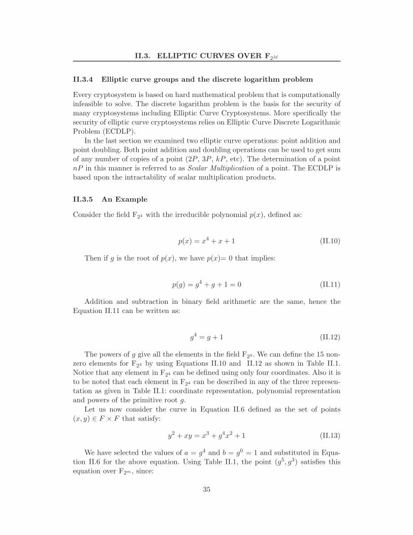
II.3. ELLIPTIC CURVES OVER F2M
II.3.4 Elliptic curve groups and the discrete logarithm problem
Every cryptosystem is based on hard mathematical problem that is computationallyinfeasible to solve. The discrete logarithm problem is the basis for the security ofmany cryptosystems including Elliptic Curve Cryptosystems. More specifically thesecurity of elliptic curve cryptosystems relies on Elliptic Curve Discrete LogarithmicProblem (ECDLP).
In the last section we examined two elliptic curve operations: point addition andpoint doubling. Both point addition and doubling operations can be used to get sumof any number of copies of a point (2P , 3P , kP , etc). The determination of a pointnP in this manner is referred to as Scalar Multiplication of a point. The ECDLP isbased upon the intractability of scalar multiplication products.
II.3.5 An Example
Consider the field F24 with the irreducible polynomial p(x), defined as:
p(x) = x4 + x + 1 (II.10)
Then if g is the root of p(x), we have p(x)= 0 that implies:
p(g) = g4 + g + 1 = 0 (II.11)
Addition and subtraction in binary field arithmetic are the same, hence theEquation II.11 can be written as:
g4 = g + 1 (II.12)
The powers of g give all the elements in the field F24 . We can define the 15 non-zero elements for F24 by using Equations II.10 and II.12 as shown in Table II.1.Notice that any element in F24 can be defined using only four coordinates. Also it isto be noted that each element in F24 can be described in any of the three represen-tation as given in Table II.1: coordinate representation, polynomial representationand powers of the primitive root g.
Let us now consider the curve in Equation II.6 defined as the set of points(x, y) ∈ F × F that satisfy:
y2 + xy = x3 + g4x2 + 1 (II.13)
We have selected the values of a = g4 and b = g0 = 1 and substituted in Equa-tion II.6 for the above equation. Using Table II.1, the point (g5, g3) satisfies thisequation over F2m , since:
35

II. Finite Fields in Cryptography
Elements in F24 Polynomial Coordinatesg0 0 (0000)g1 g (0010)g2 g2 (0100)g3 g3 (1000)g4 g + 1 (0011)g5 g2 + g (0110)g6 g3 + g2 (1100)g7 g3 + g + 1 (1011)g8 g2 + 1 (0101)g9 g3 + g (1010)g10 g2 + g + 1 (0111)g11 g3 + g2 + g (1110)g12 g3 + g2 + g + 1 (1111)g13 g3 + g2 + 1 (1101)g14 g3 + 1 (1001)g15 1 (0001)
Table II.1. Elements of the field F24 using irreducible polynomial p(x) = x4 +x+1
(g3)2 + (g3)(g5) = (g5)3 + g4(g3)2 + 1g6 + g8 = g15 + g10 + 1
(1100) + (0101) = (0001) + (1001) + (0001)(1001) = (1001)
There exists a total of fifteen points that satisfy this equation. The graphical repre-sentation of those points is shown in Figure II.7. The points are:
(1, g13), (g3, g13), (g5, g11), (g6, g14), (g9, g13), (g10, g8)(g12, g12), (1, g6), (g3, g8), (g5, g3), (g6, g8), (g9, g10),(g10, g), (g12, 0), (0, 1)
Let us now add any two points on the curve: say P = (1, g13) and Q = (g12, 0).Then by using the point addition formulae from Equation II.7 and the Table II.1,
36
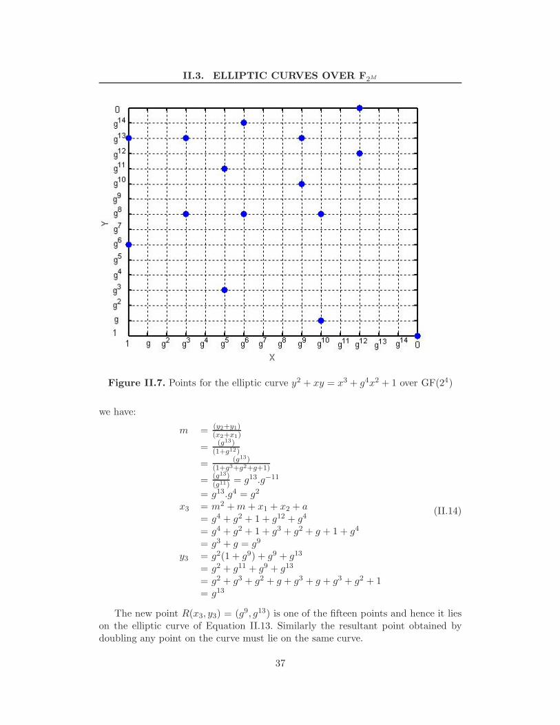
II.3. ELLIPTIC CURVES OVER F2M
Figure II.7. Points for the elliptic curve y2 + xy = x3 + g4x2 + 1 over GF(24)
we have:
m = (y2+y1)(x2+x1)
= (g13)(1+g12)
= (g13)(1+g3+g2+g+1)
= (g13)(g11)
= g13.g−11
= g13.g4 = g2
x3 = m2 + m + x1 + x2 + a= g4 + g2 + 1 + g12 + g4
= g4 + g2 + 1 + g3 + g2 + g + 1 + g4
= g3 + g = g9
y3 = g2(1 + g9) + g9 + g13
= g2 + g11 + g9 + g13
= g2 + g3 + g2 + g + g3 + g + g3 + g2 + 1= g13
(II.14)
The new point R(x3, y3) = (g9, g13) is one of the fifteen points and hence it lieson the elliptic curve of Equation II.13. Similarly the resultant point obtained bydoubling any point on the curve must lie on the same curve.
37

II. Finite Fields in Cryptography
P 2P 3P 4P 5P 6P(g3,g8) (g5,g3) (g9,g10) (1,g13) (g6,g8) (g10,g)
Table II.2. Scalar multiplication for the point P of Equation II.13
It has been mentioned earlier that there is no multiplication operation in Ellipticcurve groups. Instead the product kP is obtained by adding k copies of the samepoint P by using the addition and doubling formulas. This was called as elliptic curvescalar multiplication. An example of getting 6P for the same curve in Equation II.13and by using Table II.1 is shown in Table II.2.
II.4 Elliptic curve cryptography
In the previous sections, we described elliptic curves, their curve operations anddefined elliptic curve scalar multiplication as well as elliptic curve discrete logarith-mic problem. With this mathematical background we can now build a public-keycryptosystem based on the theory of elliptic curves. These cryptosystems are mainlyapplicable for establishing secret keys for further use in symmetrical key cryptosys-tems and the creation of digital signature as well as their digital verification. In theremaining part of this chapter, we will briefly discuss some of the most Relevantaspects in the construction and design of elliptic curve cryptosystems.
II.4.1 Elliptic curve cryptosystem parameters
Suppose that we select the elliptic curve E(Fq) as defined in the Equation II.6 andthat the underlying finite field Fq, its coefficients a, b and the order #E(Fq) of theselected curve are given. Let us select the base point P ∈ E(Fq) with a prime order kthen the private/public key pair can be defined by computing elliptic curve discretelogarithm W = sP where,
• The private key s is integer modulo k.
• The corresponding public key W is a point on the curve E(Fq).
The calculations for the public key W are directly based on the elliptic curvediscrete logarithm problem. It is therefore said that the security of this cryptosystemrelies in the difficulty of discrete logarithm problem.
II.4.2 Key pair generation
Let P is the point on the elliptic curve E(Fq) of prime order k then for the com-putation of a private/public key pair we choose first a random integer d ∈ [1, k − 1]which is a private key. After that, a public key Q is computed as:
Q = (xQ, yQ) = dP (II.15)
38

II.4. ELLIPTIC CURVE CRYPTOGRAPHY
II.4.3 Key exchange
In secret key cryptography, it is necessary that both parties at the sending andreceiving ends agree on a secret key for the transfer of messages. Fortunately keyagreement protocols exist which help in establishing a key by exchanging informationbetween two parties. It turns out that key protocols are best done using asymmetric(public key) cryptography. We present a famous protocol due to Diffie-Hellman,which provides the key establishment of a key with two message transfers. Thenit is explained how the same process can be executed using elliptic curve discretelogarithmic algorithms (ECDSA).
Diffie-Hellman key exchange: Diffie-Hellman key exchange was invented in 1976during collaboration between Whitfield Diffie, Martin Hellman and Ralph Merkleand was the first practical method for establishing a shared secret over an unpro-tected communications channel. Let A and B are already agree on a group G (mostcommonly used group G is the group of integers modulo p) and an element g in G(g mod p). Then the protocol is as follows (Figure II.8):
• A picks a random natural number a and sends ga to B.
• B picks a random number b and sends gb to A.
• A computes K=(gb)a.
• B computes K=(ga)b.
g and p are the public keys and K is the private key for the session which fromthis moment will be used for the communication between A and B. The protocol isconsidered secure if G and g are chosen properly: the eavesdropper has difficulty tocompute the element gab, because it is needed to solve the Diffie-Hellman problemrelated to discrete logarithms in order to deduce a from ga or b from gb.
Figure II.8. Diffie-Hellman protocol for key exchange
39

II. Finite Fields in Cryptography
Elliptic Curve Diffie-Hellman Key Exchange: Let A and B agree on an ellipticcurve E over a large finite field F and a point P on that curve. Then following are thesteps to exchange a secret key by using elliptic curve discrete logarithmic algorithmas shown in Figure II.9.• A and B each privately choose large random integers, denoted r1 and r2.
• Using elliptic curve point-addition, A computes r1P on E and sends it to B.B computes r2P on E and sends it to A.
• Both A and B can now compute the point r1r2P : A by multiplying the receivedvalue of r2P by his/her secret number r1, and B vice-versa.
A and B agree that the x coordinate of this point will be their shared secretvalue.
Figure II.9. Variant of Diffie-Hellamn for Elliptic Curves.
II.4.4 Digital signature scheme
Digital signatures confer three qualities on an electronic document. These are dataintegrity, authentication and non-repudiation. Successful verification of a digital sig-nature ensures the recipient that the ‘document received’ is identical to the ‘docu-ment sent’ (data integrity) and confirms the identity of the sender (authentication).It also prevents any subsequent denial by the sender that the document originatedwith them (non-repudiation).
In cryptography, digital signature schemes relay on public key encryption wheredata is signed by encrypting with private key of the sender and verified by decryptingit with the public key. A general digital signature scheme is shown in Figure II.10.
As shown in Figure II.10 a hash function (a hash function h maps bitstrings ofarbitrary finite length to strings of fixed length, say n bits. MD5 and SHA-1 are twoexamples of hash functions) is applied to the message to add an extra informationto the document which is then signed by encrypting it with the private key of thesender: the signature part of the message. The signature is annexed to the originalmessage and sent to the destination. On the receiving end, both parts: the message
40

II.4. ELLIPTIC CURVE CRYPTOGRAPHY
Figure II.10. A general digital signature scheme
and the signature are separated. The same hash function is applied to the receivedmessage to get λ1 and the signature is verified by performing the decryption usingthe public key of the signer obtaining λ2. If λ1 = λ2, then is said that message hasnot changed during transmission and the origin of the message is also confirmed.
Digital signature with ECDSA: Elliptic Curve Digital Signature Algorithm(ECDSA) is the elliptic curve analogue of the Digital Signature Algorithm (DSA).It was accepted in 1999 as an ANSI standard, and was accepted in 2000 as IEEE andNIST standards. Unlike the ordinary discrete logarithm problem and the integer fac-torization problem, no subexponential-time algorithm is known for the elliptic curvediscrete logarithm problem. For this reason, the strength-per-key-bit is substantiallygreater in an algorithm that uses elliptic curves.
The following is the procedure to digitally sign a message with ECDSA. Only aprivate key holder can perform digital signature.
1. Let M be the message then a compressed version of M is obtained using Hashfunction, e = H(M).
2. A random integer n ∈ [1, k − 1] is selected which is secret and valid for thespecific message only.
3. A point on the curve is obtained using n, (x1, y1) = nP .
4. Using the field element x1 from the last step, generate,
r = x1 (mod k) (II.16)
and
s = n−1(e + dr) (mod k) (II.17)
41

II. Finite Fields in Cryptography
The signature for this message is the pair (r, s). It is to be noted that thesignature depends on the private key and the message. This implies that no onecan substitute a different message for the same signature.
Verification: On the receiving end, the recipient can verify the signature using thereceived signature’ s values and the public key Q of the singer. Let us call the receivedpair (r′, s′). The signature has been verified if the received pair (r′, s′) is equal tothe pair (r, s). The following is the procedure for the signature’ s verification.
1. Verify that r′ and s′ are between [1, k − 1], if not, the signature is rejected.
2. Using hash function, compute e′ = H(M ′).
3. Compute
c = (s′)−1 (mod k)u = (e′)c (mod k) (II.18)v = (r′)c (mod k)
4. Compute the point (x, y) = uP + vQ. If this point is the point at infinity, thesignature is rejected.
5. Compute w = x (mod k).
6. If r′ = w, the signature is valid and the process of verification ends.
II.5 Symmetric vs asymmetric cryptography
In the last section, it has been explained the various applications (signature, verifica-tion, key exchange) of elliptic curve cryptography which is an asymmetric or publickey version of cryptography. The other variants of the same protocols using otherasymmetric ciphers like RSA have been used in the industry since long time. Thosealgorithms are based on complicated mathematical problems, which are infeasible tosolve in a considerable time period. On the other hand, symmetric ciphers are basedon well understandable mathematical problems, which contribute to the algorithmicstrength and can efficiently be implemented on both software and hardware plat-forms. That especial characteristic of symmetric ciphers makes them suitable for theencryption of large amount of data at high speed. Both the symmetric and asymmet-ric cryptography therefore have their unique applications in worldwide industries.In fact, for a large number of applications where symmetric cryptography plays avital role for rapid encryption, asymmetric encryption works at the same time todecide the session keys and to provide other features like authentication. In short,both symmetric and asymmetric cryptosystems have their specific applications andalso they are used together for the safe communications on insecure networks. Thisthesis therefore addresses rapid implementations of cryptographic algorithms fromboth symmetric and asymmetric cryptography.
42

Chapter III
General Guidelines for
Implementing Block Ciphers in
FPGAs
This chapter provides general guidelines for the implementation of block ciphersin reconfigurable logic platform. The general structure and the design principles forblock ciphers are discussed. Basic primitives in block ciphers are identified and someuseful design techniques are devised for efficient implementations on reconfigurabledevices. The chapter presents Data Encryption Standard (DES) as a case of study. Areconfigurable implementation of DES has been carried out using the same guidelinesin this chapter achieving a throughput of 274 Mbits/s occupying just 165 CLB slicesfor DES one round implementation.
III.1 Introduction
Block ciphers are based on well-understood mathematical problems using non-linearfunctions and linear modular algebra [56].
Most of the block ciphers have regular structure: same building block is repeatedmultiple times. Generally, block ciphers are of symmetric nature: the encryption anddecryption only differ in the way of using the key so that the same device can beused for both encryption and decryption.
Implementation of block ciphers mainly use bit-level operations and table look-ups. Bit-wise operators (XORs, AND/OR, etc.), substitutions, logical shifts andpermutations are quite common operations. Such operations are well suited for fastexecution in reconfigurable hardware platform (FPGAs). Furthermore, currentlyabundant memory resources in FPGAs enhance encryption speed for the operations
43

III. General Guidelines for Implementing Block Ciphers in FPGAs
like substitution. Highly parallel architectures can be designed in reconfigurablehardware achieving higher performance compared to software implementations.
In this chapter, we analyze basic characteristics of block ciphers and we exploreabout general strategies for implementing them in reconfigurable logic platform. Wesearch for the most frequent operations involved in block ciphers and we developstrategies for their implementations in reconfigurable devices. It is also explainedhow the bit level parallelism is exploited for block ciphers using either iterativeor pipeline approaches. We present a case of study for Data Encryption Standard(DES), which can be extended to the other similar cryptosystems.
DES is the most popular example in the field of block ciphers [26, 32], which wasdeveloped by IBM in the mid-seventies. The DES algorithm is organized in repetitiverounds composed of several bit-level operations such as logical operations, permu-tations, substitutions, shift operations, etc. Although those features are naturallysuited for efficient implementations on reconfigurable devices FPGAs, DES imple-mentations can be found on all platforms: software [26, 32, 46, 19, 18], VLSI [29, 28,102] and reconfigurable hardware using FPGA devices [49, 103, 45, 13, 55, 102, 71].In this Chapter, we present an efficient and compact DES architecture especiallydesigned for reconfigurable hardware platforms.
The rest of this Chapter is organized as follows: Section III.2 describes the gen-eral structure and design principles for block ciphers. Some useful properties for theimplementation of block ciphers in reconfigurable platform are also discussed in thisSection. An introduction to Data Encryption Standard (DES) is presented in Sec-tion III.3. A description of encryption and key scheduling processes using DES is alsoprovided in this Section. In Section III.4, design procedure and the design techniquesfor an FPGA architecture are described first, followed by DES implementation inFPGAs. Finally, conclusions are made in Section III.5.
III.2 Block ciphers
In cryptography, a block cipher is a type of symmetric key cipher which operateson groups of bits of a fixed length, called blocks. Block sizes are typically 64 or 128bits, though some block ciphers have a variable block size. DES is a typical exampleof block ciphers, which operates on 64-bit block. Modern block ciphers operate onblock length of 128 bits or more. Rijndael (new Advanced Encryption Standard)allows block lengths of 128, 192, or 256 bits. A block cipher makes use of a key forboth encryption and decryption. The key length not necessary to matches the blocksize of the input data. In 3DES (a variant of DES), a 64-bit block length is allowedusing a key of 192-bit (three keys of 64-bit each) for encryption and decryption.Rijndael allows the various combinations of 128, 192, and 256 bits. Block length ofless than 80 bits is not recommended for current security applications [65].
In the rest of this Section, general structure and the design principles for theblock ciphers are explained. Basic primitives in block ciphers are discussed. Finally,the implementation considerations are made in general for the hardware platformsspecifically for reconfigurable type of hardware.
44

III.2. BLOCK CIPHERS
III.2.1 General structure of a block cipher
As shown in Figure III.1, there are three main building blocks for a block cipher:block cipher encryption, block cipher decryption, and key schedule. The input isplaintext for a block cipher encryption and the output is ciphertext. Block cipherdecryption takes ciphertext as input and converts back to plaintexts. A number ofrounds are performed for a single encryption/decryption of a block. Each round usesa round key which is derived from cipher key through a process called key scheduling.Key schedule is occupied for both block cipher encryption and decryption. Thegeneral structure of a block cipher involves three main building blocks:
Figure III.1. General structure for a block cipher
1. Block cipher encryption: Most of the block ciphers are Fiestel [94] ciphers.Fiestel ciphers divide input into two halves and then two halves of the datapass through n rounds of processing. In the final round, the two halves arecombined to produce the ciphertext block. All rounds have the same structure.Each round uses a round key, which is derived from the cipher key. In generalall the round keys are different from each other and from the cipher key. Mostof the block ciphers partial or completely follow the same Fiestel structure.DES is a perfect Fiestel cipher. Modern block ciphers also repeat n roundsof the algorithm but they do not divide the input block into two halves. Allthe rounds of the algorithm are generally similar. The round transformationnormally includes the basic operations of substitution and permutation, whichapply non-linear transformations to strength the algorithm against the currentcryptanalytic attacks.
2. Block cipher decryption: Fiestel ciphers use the same structure for bothencryption and decryption. Modern block ciphers however maintain symmetricnature of the algorithm but use different critical path for decryption, that is,
45

III. General Guidelines for Implementing Block Ciphers in FPGAs
for each operation there is a reverse operation but the number of operationsremains the same.
3. Key schedule: The round keys are derived from the user key through aprocess called key scheduling. Generally, block ciphers occupy the same stepsfor the derivation of round keys for both encryption and decryption or theround keys for encryption can be used for decryption in reverse order.
III.2.2 Design principles for a block cipher
As knowledge of cryptanalysis has been evolved and as the need for both softwareand hardware encryption has emerged, advances have been shown in the design-ing new block ciphers to comply with the current security requirements. In thissubsection, we analyze some key features in designing of a block cipher.
1. Key size: If the block cipher is designed to be highly resistant against bruteforce attack, then its strength is determined by its key length: the longerthe key, the longer its takes against brute force search. Modern block ciphersemploy key lengths of 128 bits or more. A key length of less than 80 bits isnot sufficient for the current security requirements [65].
2. Variable key length: The encryption speed may be reduced by increasing keylength. Modern block ciphers offer variable key lengths to tradeoff the securityand encryption speed. Blowfish, CAST, Mars, Rijndael provide a variable keylength.
3. Mixed operations: The complication against cryptanalysis arise with theuse of more than one arithmetic and/or Boolean operator in a block cipher.This approach provides non-linearity as an alternative to S-boxes and also tointroduce non-linearity in S-Boxes. S-boxes substitute or transform input bitsinto output bits. Almost all modern block ciphers use mixed operators.
4. Variable number of rounds: Increasing the number of rounds increases thecryptanalytic strength, but also increases encryption/decryption time. Modernblock ciphers provide variable number of rounds to allow the user to make atradeoff between security and execution speed. Considering number of roundsfor a block cipher, the strength of an algorithm is interlinked with the otherdesign parameters. For example, AES with 10 rounds provides higher securitylevel as compared to DES with 16 rounds.
5. Variable plaintext/ciphertext block length: A longer block length yieldsgreater cryptographic strength. Also, a variable block length can provide ameasure of convenience, allowing the algorithm to be tailored to the applica-tion. RC5 adopts this strategy.
46

III.2. BLOCK CIPHERS
DES Blowfish IDEA AES MARS RC6 Serpent TwoFishPropertiesBlock 64 64 64 128- 128 128 128 128length 256Key 64 32- 128 128- 128- 128- 256 128-length 448 256 448 256 192No. of 16 16 8 10- 32 20 32 16rounds 14Software
√ √ √ √ √ √ √Hardware
√ √ √ √ √ √ √Symmetric
√ × × × × √Bit-wise
√ √ √ √ √ √ √ √operationsPermutation
√ × × × × √ √S-Box
√ √ × √ √ × √ √Shift or
√ √ √ √ √ √ √rotationFast Key
√ × √ √ √ √ √ √setup
Table III.1. Key features for some famous block ciphers
6. Fast key setup: In Blowfish, a lengthy key schedule algorithm was used. Thegeneration of round keys takes much longer than a single encryption/decryption.As a result, an effort to brute force attacks is greatly magnified. However,fast key setup is strongly required where the keys are required to be changedrapidly. For example, the encryption of Internet protocol (IP) packets in In-ternet Protocol Security, the overhead due to key setup may become quiterelevant. Modern block ciphers offer simple and fast key schedule algorithm.The key schedule algorithm in Rijndael is such an example.
7. Software/Hardware implementations: Modern block ciphers are designedto be implemented for both the software and hardware platforms. That impliesthe use of those arithmetic and logical operations likely to be implemented onboth the platforms offering high encryption speed. It is in fact a need for thecurrent security applications.
8. Simple arithmetic/logical operations: Perhaps, this characteristic can beseen in most block ciphers. Modern block ciphers also maintain this feature asthey include simple bit-wise operations. The algorithms are simple but strongenough against known crypto attacks.
Table III.1 describes key features for some famous block ciphers including fivefinalists (AES, MARS, RC6, Serpent, Twofish) for the competition of new AdvancedEncryption Standard. It can be seen that modern block ciphers use high block
47

III. General Guidelines for Implementing Block Ciphers in FPGAs
lengths of 128 bits or more. Similarly they provide high key lengths up till 448 bits.Both block and key lengths in block ciphers are often variable to trade the securityand speed for the chosen algorithm. Number of rounds ranges from 8 to 32, theyare fixed for some block ciphers but they can vary depending on the chosen blockand key lengths. Most block ciphers can efficiently be implemented in software andhardware platforms. All block ciphers generally include bit-wise (XOR, AND) andshift or rotate operations. Excluding few block ciphers, most of them use S-boxes forsubstitution. Fast key set-up is an important feature among modern block ciphers.They are not symmetric, that is, same building blocks used for encryption cannotbe used for decryption. Normally, each step for encryption has its own inverse fordecryption.
III.2.3 Useful properties for implementing block ciphers in FPGAs
Hardware implementations are intrinsically more physically secure: key access andalgorithm modification is considerably harder and some properties of symmetric-keycryptographic algorithms well match their implementation on reconfigurable deviceslike FPGAs.
1. Bit-wise operations: Almost all the block ciphers include bit-level opera-tions: XOR, AND, OR, etc. The abundance of bit-level operations in crypto-graphic algorithms makes their execution faster on FPGAs and additionallythey occupy relatively less hardware resources. The basic unit in FPGAs is alogic cell (LC) which provides a 4-input/1-ouput configuration for many fam-ilies of FPGA devices. This useful feature of FPGAs allow to build 2,3, or 4input and 1 output Boolean logic using the same hardware resources as shownin Figure III.2.
Figure III.2. Same resources for 2,3,4-in/1-out Boolean logic in FPGAs
2. Substitution: Substitution is an important operation in symmetric block ci-phers to add maximum non-linearity. Substitution is usually built as a look-uptable called S-Box. The strength of DES is mainly considered due to its sub-stitution boxes (S-Boxes). AES S-Box is used for both encryption/decryption
48

III.2. BLOCK CIPHERS
and key schedule algorithms. FPGAs offer three solutions for the implemen-tation of substitution operation as shown in Figure III.3. a) The logic cell(LC) of an FPGA can be configured into memory mode. In fact, a functiongenerator (FG) in an LC is implemented as a 4-input Look Up Table (LUT)(see Section I.7.1). A 4-in/1-out LUT provides 4 × 1 memory. Large numberof LUTs can be combined into a big memory. This is a fast approach becausethe pre-computed values for the S-Box can be stored saving the computationaltime for S-Box manipulation. b) The Boolean logic for substitution operationcan be implemented by configuring LCs in logic mode. It would be slow due tolarge routing overheads among a large number of LCs. 3) Some FPGA devicescontain built-in memory modules, BRAMs (Block RAMs). Those are fast ac-cess memories which do not make use of LCs and consequently with minorrouting overheads. This approach is similar but fast as compared to the op-tion (a). Only the Virtex series devices contain BRAMs. Virtex series devicescontain more than 280 BRAMs of 4K each [8].
Figure III.3. 3 approaches for the implementation of S-Box in FPGAs.
3. Permutation operation: Permutation is a common operation among blockciphers. Fortunately, there is no cost associated with it since it does not makeuse of FPGA resources and therefore consume no time for its executions.Permutation is just rewiring and the bits are rearranged (concatenated) ac-cording to the required order. Figure III.4 demonstrates a simple example ofpermutation operation for 6 bits only. The same strategy is extended for thepermutation operation over longer blocks.
4. Shift & Rotation operations: Shift is simpler than the permutation opera-tion. Shift operation is normally executed to achieve some particular data bitsor bytes, for example, retrieving 6-bit shorter blocks from 48-bit block to passthrough substitution operation in DES. In this case, shorter blocks are madeby dividing longer bus to a number of shorter buses as shown in Figure III.5a.
49

III. General Guidelines for Implementing Block Ciphers in FPGAs
Figure III.4. Permutation operation in FPGAs.
In some cases, the input data is shifted n bits and n zeroes are added, calledas zero padding. In FPGAS, zero padding for n bits is achieved by simplyconnecting n bits to the ground as shown in Figure III.5b. Most block ciphers(AES, RC6, DEAL, etc.) use rotation operation. It is similar to shift operationbut no zero padding is used. Instead, bits are moved according to a definedsetup. For example, for a 4-bit buffer, shifting left a0a1a2a3 by 1-bit is a1a2a30while rotating left by 1-bit is a1a2a3a0. Fixed rotation is trivial and there is nocost associated with it. Variable rotation is also used by some cryptographicalgorithms (RC5, RC6, CAST) however this is not a trivial operation.
Figure III.5. Shift operation in FPGAs.
5. Iterative design strategy: Block ciphers are of iterative nature, that is, niterations of the same algorithm are made for a single encryption/decryption.An iterative design strategy would be a straightforward approach which im-plements the algorithm and executes n iterations of it by consuming n clockcycles for a single encryption/decryption as shown in Figure III.6. Obviously,it is an economical approach with respect to the hardware area and the costhas to be paid in terms of design speed which gets reduced with a factor ofn. Such architectures would be useful for applications where hardware area islimited and speed is no more critical.
6. Pipeline design strategy: If reconfigurable platform is the choice for the
50

III.2. BLOCK CIPHERS
Figure III.6. Iterative design strategy.
implementation of a block cipher, a high speed architecture would result byimplementing n rounds of the algorithm as modern FPGAs are bigger enoughto accommodate massive circuits. This is called loop unrolling or pipelineapproach as shown in Figure III.7. Registers are provided between two con-secutive rounds, which operate with the same clock cycle. Once the pipeline isfilled, the output blocks therefore appear at each successive clock cycle. Thisis a fast approach but costly in terms of hardware area.
Figure III.7. Pipeline design strategy.
7. Sub-pipelining design strategy: FPGAs provide large number of flip-flops,which can be used to put several registers inside the different steps of a singleround for a pipeline design strategy. This improves the performance of pipelinearchitecture as those registers shift the internal results of a round while thefinal results are being transferred to the next round. It has been observed thatcareful use of those registers inside a round causes a significant increase indesign performance. Figure III.8 represents a sub-pipeline design strategy.
Figure III.8. Sub-pipeline design strategy.
51

III. General Guidelines for Implementing Block Ciphers in FPGAs
8. Managing block size: Modern block ciphers operate on data blocks of 128bits or more. Unlike software implementations on general-purpose micropro-cessors, FPGAs permit parallel execution of the whole data block providedthere is no data dependency in the algorithm. Our experience shows that themanual search for operations, which can be executed in parallel, is always use-ful. Moreover, FPGAs offer more than 1000 external pins to be programmablefor inputs or outputs. This is advantageous when the communication is neededwith several peripheral devices on the same board simultaneously.
9. Key scheduling: Fast key setup is one of the characteristics of modern blockciphers. The keys are required to be changed rapidly in some cryptographicapplications e.g. the encryption of Internet protocol (IP) packets in InternetProtocol Security (IPSec). It is possible to exploit the reconfigurable featureof the FPGAs to configure for various keys rapidly.
10. Key storage It is recommendable for cryptographic applications to make useof different secret keys for different sessions. FPGAs provide enough memoryresources to store various session keys. As the keys are stored inside an FPGA,it is therefore valid to say that FPGA implementations are physical secure.
III.3 Data Encryption Standard
On August, 1974, IBM submitted a candidate (under the name LUCIFER) for cryp-tographic algorithm in response to the 2nd call from National Bureau of Standards(NBS), now the National Institute of Standards & Technology (NIST)[65], to pro-tect data during transmission and storage. NBS launched an evaluation process withthe help of National Security Agency (NSA) and finally adopted a modification ofLUCIFER algorithm as the new Data Encryption Standard (DES) on July 15, 1977.The Data Encryption Standard [105], known as Data Encryption Algorithm (DEA)by the ANSI [105] and the DEA-1 by the ISO [43] remained a worldwide standardfor a long time until it was replaced by the new Advanced Encryption Standard(AES) on October 2000. However, it is expected that DES will remain in the publicdomain for a number of years. It provides a basis for comparison for new algorithmsand it is still used in IPSec protocols, ATM encryption, the secure socket layer (SSL)protocol and in TripleDES. A detail description of DES algorithm can be seen at[90, 56, 97]. A brief introduction about DES in this chapter is mainly based on [90].
DES uses a 64-bit block for the key; however, 8 of these bits are used for oddparity and are, therefore, not counted in the key length. The effective key lengthis then calculated as 56 bits, giving 256 possible keys. DES is a block cipher: Itencrypts/decrypts data in 64-bit blocks using a 64-bit key. DES is a symmetricalgorithm: The same algorithm and key are used for both encryption and decryption.DES is an iterative cipher: the basic building block (a substitution followed by apermutation) called a round is repeated 16 times. For each DES round, a sub-key is derived from the original key through a process called key scheduling. Key
52

III.3. DATA ENCRYPTION STANDARD
scheduling algorithm for encryption and decryption is the same however round keysfor decryption are used in reverse order. Figure III.9 demonstrate the basic algorithmflow for both the encryption and key schedule processes.
Figure III.9. DES Algorithm
Encryption begins with an initial permutation (IP), which scrambles the 64-bitplain-text in a fixed pattern. The result of the initial permutation is sent to two 32-bitregisters, called the right half register, R0 and left half register, L0. Those registershold the two halves of the intermediate results through succeeding 16 iterations of
53

III. General Guidelines for Implementing Block Ciphers in FPGAs
the function fk which is given by (n = 0 to 15):
Ln = Rn−1
Rn = Ln−1 + f(Rn−1,Kn)(III.1)
After 16 iterations, the contents of the right and left half registers are subjected toa final permutation IP−1, which is the inverse of the initial permutation. The outputof IP−1 is the 64-bit ciphertext. A detailed explanation of those three operations isprovided in the rest of this Subsection followed by the process of generating sub-keysfrom the original key.
III.3.1 The initial permutation (IP−1)
The initial permutation is the first operation applied to the input block beforeiteration 1. It transposes the input block as described in Table III.2. For example,the initial permutation moves bit 58 to bit position 1, bit 50 to bit position 2, bit42 to bit position 3, and so forth. The initial permutation has no effect on DESsecurity and its primary purpose is to make it easier to load plain-text into a DESchip in a byte-sized pieces. Implementing it in hardware is trivial but cumbersomein software.
58 50 42 34 26 18 10 260 52 44 36 28 20 12 462 54 46 38 30 22 14 664 56 48 40 32 24 16 857 49 41 33 25 17 9 159 51 43 35 27 19 11 361 53 45 37 29 21 13 563 55 47 39 31 23 15 7
Table III.2. Initial permutation for 64-bit input block
III.3.2 Structure of the function fk
The 64-bit output from the initial permutation is divided into two halves L0 of 32bits and R0 of 32 bits, as shown in Figure III.9. Both halves go through the 16iterations of the function fk (Eq. III.1) which is described as follows:
For the first iteration, R0 of 32 bits and 48-bit round key are the two inputs.We first expand R0 from 32 bits to 48 bits by using the expansion permutation(Permutation E).
54

III.3. DATA ENCRYPTION STANDARD
32 1 2 3 4 5 4 5 6 7 8 98 9 10 11 12 13 12 13 14 15 16 1716 17 18 19 20 21 20 21 22 23 24 2524 25 26 27 28 29 28 29 30 31 32 1
Table III.3. E-bit selection
The Expansion Permutation (Permutation E)
This operation expands right half 32-bit to 48 bits. Some bits are therefore repeatedand the order of the bits is also changed as shown in Table III.3.
Table III.3 shows the position relationship between inputs and outputs. Forexample, the bit in position 3 of input block moves to position 4 of the outputblock, and the bit in position 21 of the input block moves to position 30 and 32 ofthe output block. The repeated bits and their positions in output block can easilybe seen as they are outside the squares in boldface letter as shown Table III.3.
This operation has two purposes. First, it makes the size of right half registerequal to key size for XOR operation. Second, it provides longer result that can becompressed during substitution operation.
The output 48-bit is XORed with the 48-bit round key. We now have 48 bits, oreight groups of six bits. The six bits of eight groups are used as addresses in tablescalled, S-Boxes. Each group of six bits is substituted to a group of 4 bits.
The S-Box substitution
DES S-box is 64-entry table arranged into four rows and sixteen columns. The inputis 6-bit address and output of each S-box is 4-bit long. This way, the first and last bitsa0a5 of 6-bit address a0a1a2a3a4a5 represent the row number while the middle fourbits a1a2a3a4 denote the column number. Hence the S-box will substitute 101011,the entity located at row 4th (11) and column 6th (0101). To substitute 48-bit input,DES contains eight S-boxes each of size 64 × 4 = 256 bits occupying a total of 2kmemory as shown in Table III.4
The 32-bit S-Box output undergoes through another permutation, which is calledP-Box Permutation.
The P-Box permutation
This is called straight permutation or just permutation. The 32-bit output of theS-box substitution is permutated according to P-box as shown in Table III.5. Ta-ble III.5 shows the position to which each bit moves. For example, bit 21 moves tobit 4, while bit 4 moves to bit 31. No bits are used twice and no bits are ignored.
The output 32-bit after this permutation is XORed with the 32-bit of L0, achiev-ing R1. This is the end of first iteration. Let us remember that all the operationswere executed on the contents of 32-bit register R0 and we achieve R1. In the next
55

III. General Guidelines for Implementing Block Ciphers in FPGAs
ColumnRow 0 1 2 3 4 5 6 7 8 9 10 11 12 13 14 15 S-Box
0 14 4 13 1 2 15 11 8 3 10 6 12 5 9 0 71 0 15 7 4 14 2 13 1 10 6 12 11 9 5 3 8 S1
2 4 1 14 8 13 6 2 11 15 12 9 7 3 10 5 03 15 12 8 2 4 9 1 7 5 11 3 14 10 0 6 13
0 15 1 8 14 6 11 3 4 9 7 2 13 12 0 5 101 3 13 4 7 15 2 8 14 12 0 1 10 6 9 11 5 S2
2 0 14 7 11 10 4 13 1 5 8 12 6 9 3 2 153 13 8 10 1 3 15 4 2 11 6 7 12 0 5 14 9
0 10 0 9 14 6 3 15 5 1 13 12 7 11 4 2 81 13 7 0 9 3 4 6 10 2 8 5 14 12 11 15 1 S3
2 13 6 4 9 8 15 3 0 11 1 2 12 5 10 14 73 1 10 13 0 6 9 8 7 4 15 14 3 11 5 2 12
0 7 13 14 3 0 6 9 10 1 2 8 5 11 12 4 151 13 8 11 5 6 15 0 3 4 7 2 12 1 10 14 9 S4
2 10 6 9 0 12 11 7 13 15 1 3 14 5 2 8 43 3 15 0 6 10 1 13 8 9 4 5 11 12 7 2 14
0 2 12 4 1 7 10 11 6 8 5 3 15 13 0 14 91 14 11 2 12 4 7 13 1 5 0 15 10 3 9 8 6 S5
2 4 2 1 11 10 13 7 8 15 9 12 5 6 3 0 143 11 8 12 7 1 14 2 13 6 15 0 9 10 4 5 3
0 12 1 10 15 9 2 6 8 0 13 3 4 14 7 5 111 10 15 4 2 7 12 9 5 6 1 13 14 0 11 3 8 S6
2 9 14 15 5 2 8 12 3 7 0 4 10 1 13 11 63 4 3 2 12 9 5 15 10 11 14 1 7 6 0 8 13
0 4 11 2 14 15 0 8 13 3 12 9 7 5 10 6 11 13 0 11 7 4 9 1 10 14 3 5 12 2 15 8 6 S7
2 1 4 11 13 12 3 7 14 10 15 6 8 0 5 9 23 6 11 13 8 1 4 10 7 9 5 0 15 14 2 3 12
0 13 2 8 4 6 15 11 1 10 9 3 14 5 0 12 71 1 15 13 8 10 3 7 4 12 5 6 11 0 14 9 2 S8
2 7 11 4 1 9 12 14 2 0 6 10 13 15 3 5 83 2 1 14 7 4 10 8 13 15 12 9 0 3 5 6 11
Table III.4. DES S-boxes
16 7 20 21 29 12 28 17 1 15 23 26 5 18 31 102 8 24 14 32 27 3 9 19 13 30 6 22 11 4 25
Table III.5. Permutation P
iteration, we will have L2 = R1, which is the block we just calculated and then wemust calculate R2, repeating the same procedure as was used for R0 and so on for16 iterations. At the end of the 16th iterations we have the blocks L16 and R16. Theorder of these blocks is reversed and two blocks are concatenated into a 64-bit blockR16L16. A final permutation IP−1 is then applied.
The Final permutation
This permutation is exactly inverse of the initial permutation and is described inTable III.6. Referring to Fig. III.9, left and right halves are not changed after the
56

III.3. DATA ENCRYPTION STANDARD
last round of DES, instead the concatenated block R16L16 is used as input to thefinal permutation. Exchanging halves and shifting around the permutation wouldyield the same results. This way, the same algorithm can be used for both encryptionand decryption.
40 8 48 16 56 24 64 3239 7 47 15 55 23 63 3138 6 46 14 54 22 62 3037 5 45 13 53 21 61 2936 4 44 12 52 20 60 2835 3 43 11 51 19 59 2734 2 42 10 50 18 58 2633 1 41 9 49 17 57 25
Table III.6. Inverse permutation
This completes the encryption process for a single block. Decryption is simplythe inverse of encryption, following the same steps as above, but reversing the orderin which the sub-keys are applied.
III.3.3 Key schedule
The sub-keys for all the 16 rounds are derived from the original key as shown inFigure III.9. First the 64-bit DES key is reduced by ignoring every 8th bit governedby the Table III.7 (Permuted Choice One PC-1). After 56-bit key is extracted, the
57 49 41 33 25 17 9 1 58 50 42 34 26 1810 2 59 51 43 35 27 19 11 3 60 52 44 3663 55 47 39 31 23 15 7 62 54 46 38 30 2214 6 61 53 45 37 29 21 13 5 28 20 12 4
Table III.7. Permuted choice one PC-1
48-bit sub-keys for all rounds are generated as follows:The 56-bit key is divided into two halves C0 and D0. At each round, the two
halves are subjected to a circular left shift or rotation by either one or two bits,depending on the round as given in Table III.8.
Round No. 1 2 3 4 5 6 7 8 9 10 11 12 13 14 15 16Bits shifted 1 1 2 2 2 2 2 2 1 2 2 2 2 2 2 1
Table III.8. Number of key bits shifted per round
57

III. General Guidelines for Implementing Block Ciphers in FPGAs
The shifted values serve as input to the next round and also serve as input tothe Permutated Choice Two (PC-2) as given in Table III.9. The resulting 48 bits isthe required round key.
14 17 11 24 1 5 3 28 15 6 21 1023 19 12 4 26 8 16 7 27 20 13 241 52 31 37 47 55 30 40 51 45 33 4844 49 39 56 34 53 46 42 50 36 29 32
Table III.9. Permutated choice two (PC-2)
III.4 FPGA implementation of DES algorithm
In this section DES implementation is described on reconfigurable hardware plat-form. All the design steps for the development of FPGA architecture are explained.Some useful design techniques for the improvement of design performance are illus-trated. Performance results and comparison with the previous FPGA implementa-tions of DES are presented at the end of this Section.
III.4.1 Design steps
In general, most of the design tools follow the basic six steps for an FPGA designas shown in Fig. III.10. Those steps are not executed in a specific order but theycan be repeated to improve design’s performance. A short description of each stepis provided below.
Figure III.10. Design flow
1. Design Entry : There are two standard ways to specify a design on FPGA.
58

III.4. FPGA IMPLEMENTATION OF DES ALGORITHM
• Design Entry through HDLs (Hardware Description Languages): A De-signer can describe an FPGA design in high-level abstract language likeVHDL (Very high speed integrated circuit Hardware Description Lan-guage) or Verilog. Those languages are ideal to build state machines,combinational logic, complex and large designs. All the existing softwaremanagement methods well hold for those languages as any change or mod-ification is being treated like in other traditional languages. However, thisreally depends on the quality of the tools used for synthesis.
• Design Entry through Schematic: An FPGA design can also be describedby using library components of the devices through a graphical interface.It is easy to optimize a circuit for speed/area and consequently it savestime and efforts of the design tool in hardware mapping, placement androuting, etc. However, it is hard to debug and modifications to the designare not straightforward as compared to design entry through HDLs.
2. Functional verification and simulation: It checks the logical correctnessof an FPGA design. After the design has been represented by using HDLsor schematic, it is necessary to verify if such description meets the designspecifications.
3. FPGA synthesis: Synthesis converts design entry into gates/blocks of anFPGA device. A netlist of basic gates is prepared from HDL/schematic designentry, which is further optimized at gate level. The next step is to map netlistinto FPGA real resources. This is an important step based on design entry.An FPGA designer must keep in mind the basic structure of the target devicewhile writing HDL code or using schematic libraries of the device for designentry.
4. FPGA place and route: Place and route selects the optimal position forelementary design blocks and minimal interconnection distance between them.Place and route tools normally use device vendor specifications. Usually theyprovide hand-placement and also automatic features for optimizing criticalpaths for speed or area.
5. Circuit analysis: Circuit analysis determines different features of the cir-cuit related to efficiency. Timing verification is made which may differ fromfunctional simulation as it provides logical correctness taking into account allcircuit delays occurring in the real device. Similarly, power analysis providespower consumption by the circuit. There exist special tools to determine andto improve such type of circuit features.
6. Programming FPGA device: Programming FPGA implies downloadingbit stream codes from the last steps onto the target FPGA device. Universalprogramming tools work with FPGAs from different vendors. However there
59

III. General Guidelines for Implementing Block Ciphers in FPGAs
are dedicated programming tools bounded only with a single family of FPGAdevices.
III.4.2 Design techniques
Here we discuss few design techniques, in general for symmetric-key block ciphersand in particular for DES on FPGAs. It has been observed that better design tech-niques for both design entry and design implementation play an important role foroptimizing circuits. A short description of those optimizing techniques is providedhere.
• Design strategy: Design strategy is application dependent. Time criticalapplications care of timings and other factors like hardware resources or cost ofthe device are of secondary importance. Cryptographic algorithms (especiallyblock ciphers) have iterative nature and n iterations of the same algorithmare made. It is therefore possible to implement just one round and consume ncycles (iterative looping) or implement n rounds of the algorithm (pipelining)to achieve high timing performances. DES has 16 rounds.
• Choice of target device: The choice of the target device (FPGA) is basedon the design strategy. A large number of FPGAs are available in the mar-ket by various manufacturers. The basic structure of all FPGAs is the samehowever some of them offer additional features like built-in-memories, built-in-arithmetic functions, etc. FPGAs are of different sizes depending on the prices.For DES implementation, the chosen target device XCV400fg456 belongs toVirtexE family of devices. Virtex and VirtexE family of devices contains morethan 280 built-in memory modules called as BlockRAMs (BRAMs). Thosememories are fast access memories and can be occupied for DES SP-boxes.However, due to small memory requirements, BRAMs were not used. Instead,FPGA CLBs were configured in memory mode. In short, the selection of anFPGA depends upon the design size and design requirements.
• Design analysis: Design/algorithm analysis helps in reducing design sizeand path delays in the circuit. It may not be a good effort to implement a fastsoftware code in hardware. Software codes are often optimized for 8, 16 or 32bit general-purpose microprocessors. In hardware, such types of limitations donot exist. A bit-level parallelism can freely be exploited unless one encountersdata dependencies or resource limitations. Let us consider an instruction froma software code optimized for 32-bit general-purpose microprocessor:
work = [((left 16) | right)&0× 0000FFFF ];
which requires 16 right shifts, logical XOR and then logical AND with 0 ×0000FFFF . That instruction in software is an effort to execute an XOR op-eration for the 16 most significant bits of 32-bit ‘left’ and ‘right’ registers. In
60

III.4. FPGA IMPLEMENTATION OF DES ALGORITHM
hardware description languages, the same instruction can be implemented justcaring for language notations. One of the best option is to eliminate the ANDand 16 logical Shifts by executing XOR operation directly to the 16 most sig-nificant bits of left and right registers, that is, work = left [31:16] XOR right[31:16].
• Selecting FPGA resources: An FPGA designer can opt for multiple optionsfor performing a function. For example, two choices for implementing a 2-bitmultiplexer are shown in Figure III.11.
Figure III.11. 2-bit multiplixer using (a) Tristate Buffer. (b) LUT
Figure III.11a shows usage of tri-state buffers for a multiplexer. A large numberof tri-state buffers are available in FPGAs and it seems logical to make useof them. However, our experience shows that, using large number of tri-statebuffers slows down the circuit. It is due to physical distribution of tri-statebuffers all around FPGA, which requires long routing paths. A multiplexer canalso be implemented using LUTs as shown in Figure III.11b. Using adjacentLUTs for an n to 1 multiplexer would be useful when a circuit is required tobe optimized for speed.
Similarly, some FPGA devices contain built-in memory modules. It would beuseful to utilize those memories as they provide faster access to the data ascompared to distributed memories in FPGAs which are formed using severalLUTs.
• Hardware approach: Hardware Description Languages (HDLs) are analo-gous to other high level languages (C, C++, etc.) with some subtle differences.Both types of language are processed by a compiler. Writing style is the same.However they differ in executing compiled code. HDLs are used for formaldescription of electronic circuits. They describe circuit’s operation, its design,and tests to verify its operation by means of simulation. Compilers compile anHDL code and provide a list of electronic components in the circuit and alsogive details of how they are connected. We will focus here in writing an HDLcode for an FPGA design.
An FPGA designer can know about the components (flip-flops, tri-state buffers,LUTs) resulted by an HDL instruction. For example, an if statement in HDL
61

III. General Guidelines for Implementing Block Ciphers in FPGAs
describes a multiplexer or a flip-flop. Now, the frequent use of this state-ment would insert large number of multiplexers or flip-flops resulting a circuit,which is functionally correct but may or may not be efficient. Here, hardwareapproach, therefore, defines in thinking about the component first and thenwriting an HDL code accordingly. In other words if a programmer requires thefunctionality of a flip-flop than he can search for a suitable flip flop for thedesign and then he/she can write a code for it. That would generate a list ofcomponents for an electronic circuit prior to its implementation providing acomplete control to the designer over the used and available resources in anFPGA.
III.4.3 DES implementation on FPGAs
Figure III.12 represents a block diagram for DES implementation on FPGA. As ithas been earlier discussed that permutation is a simple operation on hardware de-vices. It can be implemented by changing bit positions for the outgoing bus (changeof wires), hence it is free of cost. DES includes lot of permutation operations (ini-tial, final, permutation E, permutation P). The building blocks for those operationsin Figure III.12 are therefore symbolic representations having no logic inside. EachS-Box in DES occupy 64×4=256-bit memory, a total of 2048 bits for eight S-Boxes.The implementation for S-Boxes consumes only 32 CLB slices configured in memorymode. Temporary registers and XOR blocks are the other operations, which occupyFPGA resources.
Figure III.12. DES implementation on FPGA
Three inputs: Chip Enable (CE), Clock (CLK), input data (IN) and the onlyoutput (OUT) are the four pins of DES chip. Chip enable (CE) activates the timinglogic as well as the rest of the circuitry, in its low state (when it is ’0’). The ex-ternal clock CLK is the master clock for the whole circuit that is used to generateall the control signals to synchronize the data flow. When CE enables the circuit,
62

III.4. FPGA IMPLEMENTATION OF DES ALGORITHM
The 64-bit at the input are permuted and divided into two halves RIN and LIN. Atthe first rising edge of the clock both halves are being transferred to the output ofthe two registers REGA and REGB. The right halves (REGA output) go through anumber of operations: Permutation E; addition with sub-key; substitution (throughS-Boxes); Permutation P and; addition with the original left half (REGB output).Before the next clock comes, the old right half (RIGHT) is the input of the registerREGB and the new left half (LEFT) is the input of the register REGA. The sixteeniterations are then executed. After 16th clock cycles the two halves RIGHT andLEFT are concatenated and the resulting block goes through the inverse permuta-tion (IP−1) resulting one encryption for a 64-bit input block. Notice that the usageof an eight DES S-Boxes parallel structure, results in a significant reduction of thecritical path for encryption/decryption.
III.4.4 Design testing and verification
DES implementation was made on XCV400e-8-bg560 VirtexE device using XilinxFoundation Series F4.1i. The design tool provides two options for design testingand verification: functional simulation and timing verification. Functional verifica-tion tests the logical correctness of the design. It is performed after the design entryhas been completed using VHDL or using library components of the target devices.It detects logical errors without considering circuit overheads like path delays, syn-chronization, etc. A netlist of the logic components in the design is created by thedesign tool, which is then mapped to the available resources of the actual targetdevice. Timing verifications are made at this stage. That is useful feature by thedesign tool to verify circuit performance taking into account all circuit overheads.Both functional and timing verifications must be performed for a successful designimplementation. For both cases, test vectors are used for the verification of theresults. Table III.10 shows the test vectors used in our DES implementations.
Input Block First Permutation f (R,K) Second permutation
LIN=0×FFFF0000 LFOUT=0×06060606 LEFT=0×49DE9DF2 LOUT=0×17F77A33RIN=0×AAAAAAAA RFOUT=0×E7E7E7E7 RIGHT=0×C7EEC966 ROUT=0×7B7AB72A
Table III.10. Test vectors
Figure III.13 and Figure III.14 show the results for the functional simulationand the timing verification for DES implementation on FPGA. Notice that thedifference between Figure III.13 and III.14. Time delays in Figure III.14 are moreclear. Timings (clock cycles) presented in Figure III.14 are the real timings for thecircuit.
III.4.5 Performance results and comparison
FPGA implementation of DES algorithm was accomplished on a VirtexE deviceXCV400e-8-bg560 using Xilinx Foundation Series F4.1i as synthesis tool. The design
63

III. General Guidelines for Implementing Block Ciphers in FPGAs
Figure III.13. Functional simulation
Figure III.14. Timing verification
was coded using VHDL language. It occupied 165 (3%) CLB slices, 117 (1%) sliceFlip Flops and 129 (41%) I/Os. The design achieves a frequency of 68.05 MHz (14.7ηS). It takes 16 clock cycles to encrypt one data block (64-bits). Therefore, theachieved throughput is (68.05 × 64)/16=274 Mbits/s.
Table III.11 shows the performance figures for some representative DES hardware
64

III.4. FPGA IMPLEMENTATION OF DES ALGORITHM
implementations. Notice that the achieved results are competitive with the existingimplementations.
Author Device Design Area (A) Freq. Throughput T/AStrategy CLB slices (MHz) (Mbits/s) (T)
Kaps and XC4028EX pipeline 741 25.18 402.7 0.54Paar [45] (4-round)Free-DES XCV400 Pipeline 5263 47.7 3052 0.57[13]McLoony et XCV1000 Pipeline 6446 59.5 3808 0.59al. [55]Patterson XCV150 pipeline 1584 168 10752 6.78(Jbits) [71] SW/HWWong et al. XC4020E Iterative 438 10 26.7 0.06[103]This work XCV400e Iterative 117 68.05 274 2.34
Table III.11. Recent DES reconfigurable hardware implementations
Several FPGA implementations of DES have been reported in the literatureachieving throughput ranges from 26 to 10752 Mbits/s. A DES implementation in[13] is a free DES core which achieves a data rate of 3052 Mbits/s using pipelineapproach in ECB mode. A java-based (Jbits) DES implementation in [71] achievesthe fastest encryption rate of 10752 Mbits/s. It implements all DES primitives inFPGA while key schedule in software. The communication between the two opera-tions is made through a Java-based Application Programming Interface (API) whichis used for the runtime creation and modification of the configuration bit-stream.FPGA implementation of DES in [45] implement both 2-stage and 4-stage pipelineapproaches obtaining throughput of 183.8 Mbits/s and 402.7 Mbits/s respectively.Almost all FPGA architectures for DES implement partial or fully pipeline ap-proaches. Only the design in [103] is a one round DES implementation on a single-chip FPGA. A fair comparison is possible with this design only. The design wasimplemented on XC4020E occupying 438 CLB slices. It takes 24 cycles to completeencryption for one single data block achieving a throughput of 26.7 Mbits/s. Hencethe Throughput/Area factor is 0.06. Our DES implementation improves both thearea and throughput factors consuming only 165 CLB slices on XCV400 showinga throughput of 274 Mbits/s. The Throughput/Area factor for our design is 2.34.Comparing our architecture with the design in [103], we get a speedup improvementof almost 10 times in throughput occupying four times less CLB slices. In fact ourdesign ranks second considering as a figure of merit the Throughput/Area Factor isreally convincing.
65
III. General Guidelines for Implementing Block Ciphers in FPGAs
III.5 Conclusions
This chapter provides a general guideline for the implementation of block ciphers inreconfigurable logic platform. The general structure of block ciphers was discussed.Most frequent operations in block ciphers were presented. Some useful properties forimplementing block ciphers in FPGAs were discussed. The design steps and somedesign techniques for an FPGA implementation were described. A general guideline,therefore, developed for the implementation of block ciphers in reconfigurable de-vices. Same guideline was then applied for DES implementation resulting an efficientand compact DES core on reconfigurable hardware platform. From Table III.11, itcan be seen that our design showed improvements both in time and area whencompared with other reported reconfigurable hardware implementations of DES.
Our architecture can be improved to offer even better results in terms of achievedthroughput. The most obvious extension is to design a fully pipelined architecturein order to obtain a higher throughput at the price of area.
66

Chapter IV
Architectural Designs For
Advanced Encryption
Standard
This chapter investigate the significance of FPGA implementations for new Ad-vanced Encryption Standard (AES). Multiple architectural implementation optionsare explored for AES. The results of each AES implementation are evaluated in aneffort to determine the most suitable candidate architecture for variety of differentcryptographic applications restricted to area or time. The performance results arewell compared with the existing FPGA implementations of AES algorithm showingsignificant improvements both in space and time.
IV.1 Introduction
On October 2000, a new Advanced Encryption Standard (AES) ‘Rijndael’ (basedon the names of two inventors ‘Rijmen’ and ‘Daemen’) was selected by NIST [65]replacing Data Encryption Standard DES. From its evaluation process to post se-lection period the algorithm has been implemented on all kind of hardware andsoftware platforms. Gladman [34] and Guido et al [17], reported software imple-mentations in which AES specification is manipulated to increase performance. AESsoftware implementations have a throughput that ranges from 300 to 800 Mbps de-pending on the specific architecture and platform selected by the developers. Someefficient AES encryptor/decryptor core VLSI implementations have been also re-ported [42, 99, 51, 79]. Performance of VLSI implementations ranges from 2 to 7.5Gbits/s.
Similarly, various AES FPGA implementations have been reported at [33, 25, 30,52]. Those are one round (iterative) or n rounds (pipeline) FPGA implementations
67

IV. Architectural Designs For Advanced Encryption Standard
optimized for encryption or encryption/decryption processes. Since FPGA devicesused in previous works are rather different, performance results are broadly variable;they range from 300 Mbps to 6 Gbit/s, approximately.
Asymmetric characteristics of AES encryption and decryption processes limit theimplementation of high-performance AES cores. Each step in AES for encryptionhas its inverse (in GF(2m)) for decryption. Designing separated architectures forencryption and decryption processes would imply the allocation of a large amount ofFPGA resources and the area requirements of such design might be even impossibleor difficult to meet in several FPGA families of devices. This is one of the reasonswhy designs reported [33, 25, 30], have considered only the encryption part of AES.Both designs at [33, 25] are one round implementations with [25] or without [33]key scheduling. The design at [30] implements all AES rounds (pipeline) withoutkey scheduling. Only the design at [52] has reported an FPGA implementation ofa fully pipeline AES encryptor/decryptor core.
In this Chapter, various FPGA implementations of AES are presented. Thoseimplementations cover all three basic processes: key scheduling, encryption and de-cryption, on a single-chip FPGA. Different design architectures are considered byimplementing AES encryptor, decryptor and encryptor/decryptor cores separately.Both iterative and pipeline techniques are applied showing time-area tradeoffs. AllAES implementations are optimized for low cost, high efficiency or high portability.The rest of this Chapter is organized as follows.
An introduction to AES algorithm is presented in Section IV.2. The differencebetween AES and Rijndael is clarified. The basic transformations of the algorithmand their effects on the algorithm cryptographic strength are also explained in thisSection. Section IV.3 describes various novel techniques for implementing AES onFPGAs. Those techniques help to improve overall algorithm performance by mod-ifying the most costly operations of the algorithm. Section IV.4 deals with AESimplementation on FPGAs by taking into account the modifications in AES trans-formations discussed in the previous Sections. Section IV.5 compares achieved resultsfollowed by conclusion remarks in Section IV.6.
IV.2 The Rijndael algorithm
Rijndael algorithm was announced as the winner of the contest for new AdvancedEncryption Standard(AES) [65, 24] by NIST [65] on October, 2000. This Sectionexplains the behavior the algorithm. First it is explained the difference betweenAES and Rijndael. Secondly, the basic structure and building blocks are described.Third, it is specified the round transformation of the algorithm. Then, key scheduleis described.
IV.2.1 Difference between AES and Rijndael
Rijndael is a block cipher algorithm with variable block and key lengths. It canprocess blocks of 128, 192, and 256 bits. All combinations of block and key lengths
68

IV.2. THE RIJNDAEL ALGORITHM
are possible. The only difference between Rijndael and AES is the supported rangeof block length and cipher key length.
key length (bits) Block length (bits)128 192 256
128 10 12 14192 12 12 14256 14 14 14
Table IV.1. Selection of Rijndael rounds
The AES fixes the block length to 128 bits and supports key lengths of 128,192 or 256 bits only. The numbers of rounds depend upon the combination of theselected block and key lengths as shown in Table IV.1. From Table IV.1, the allowednumber of rounds for this combination are 10. All over this document whenever weuse AES, it means a block and key lengths of 128 bits.
IV.2.2 Structure of the AES algorithm
The basic structure of AES algorithm is shown in Figure IV.1.
Figure IV.1. Basic structure of Rijndael algorithm.
For encryption the input is a plaintext block and a key block, and the output isciphertext block. For decryption the input is ciphertext block and a key, the outputis plaintext. The basic algorithm flow for encrypting one block of data is shown inFigure IV.2.
Figure IV.2. Basic algorithm flow.
69

IV. Architectural Designs For Advanced Encryption Standard
The AES cipher treats the input 128 bit block as a group of 16 bytes organizedin a 4× 4 matrix called State matrix. The algorithm consists of an initial transfor-mation, followed by a main loop where nine iterations called rounds are executed.Each round transformation is composed of a sequence of four transformations: Byte-Substitution (BS), ShiftRows (SR), MixColumns (MC) and
AddRoundKey (ARK). For each round of the main loop, a round key is derivedfrom the original key through a process called Key Scheduling. Finally, a last roundconsisting of three transformations BS, SR and ARK is executed. The AES decryp-tion algorithm operates similarly by applying the inverse of all the transformationsdescribed above in the reverse order.
IV.2.3 The round transformation
The round transformation [24] is a sequence of four transformations BS, SR, MC andARK. All four transformations contribute in AES strength by inducing confusionand diffusion optimalities. The confusion and diffusion are two important propertiesthat give some indication about the strength of a cryptographic system. Confusionmakes the output dependent on the key. Ideally, every key bit influences every out-put bit. Diffusion makes the output dependent on previous input (plain/ciphertext).Ideally, each output bit is influenced by every (previous) input bit. Those, roughlycorrespond to substitution and permutation. Symmetric ciphers need to be complex,so they cannot be analyzed easily. Also, they need to be simple, enough to be imple-mented efficiently achieving high encryption rates. For AES, the general criteria forround transformation was invertibility and simplicity besides the step-specific crite-ria. This Section describes all four steps of round transformation with step-specificcriteria to provide an idea how effective AES is at mixing up bits.
ByteSubstitution (BS)
It is mainly a non-linear transformation where each input byte of the State matrix isindependently replaced by another byte from a look-up table called S-Box as shownin Figure IV.3.
Figure IV.3. BS operates at each individual byte of the state matrix
70

IV.2. THE RIJNDAEL ALGORITHM
The non-linearity and algebraic complexity are the general criteria for designingAES S-Box [24]. The AES S-Box is a 256-entry table composed of two transforma-tions: First each input byte is replaced with its multiplicative inverse (MI) in GF(28)with the element {00} being mapped to itself; followed by an affine transformationover GF(2).
Multiplicative inverse can be found by means of extended Euclidean algorithm[56]. Let MI of the polynomial a(x) is desired then extended Euclidean algorithmcan be used to find two polynomials b(x) and c(x) such that:
a(x)× b(x) + m(x)× c(x) = gcd(a(x),m(x)) (IV.1)
where gcd(a(x),m(x)) represents greatest common divisor of the polynomials a(x)and m(x) which is always 1 iff m(x) is irreducible. Applying modular reduction toEquation IV.1, we get:
a(x)× b(x) = 1 mod m(x) (IV.2)
which means that b(x) is the inverse element of a(x) (by the definition of multipli-cation).
The affine transformation f is defined as follows.
y = f(x)⎡⎢⎢⎢⎢⎢⎢⎢⎢⎣
y7
y6
y5
y4
y3
y2
y1
y0
⎤⎥⎥⎥⎥⎥⎥⎥⎥⎦
=
⎡⎢⎢⎢⎢⎢⎢⎢⎢⎣
1 1 1 1 1 0 0 00 1 1 1 1 1 0 00 0 1 1 1 1 1 00 0 0 1 1 1 1 11 0 0 0 1 1 1 11 1 0 0 0 1 1 11 1 1 0 0 0 1 11 1 1 1 0 0 0 1
⎤⎥⎥⎥⎥⎥⎥⎥⎥⎦×
⎡⎢⎢⎢⎢⎢⎢⎢⎢⎣
x7
x6
x5
x4
x3
x2
x1
x0
⎤⎥⎥⎥⎥⎥⎥⎥⎥⎦⊕
⎡⎢⎢⎢⎢⎢⎢⎢⎢⎣
01100011
⎤⎥⎥⎥⎥⎥⎥⎥⎥⎦
(IV.3)
The non-linearity is introduced by applying multiplicative inverse in GF(28).The affine transformation has no impact on the non-linearity but contribute in al-gebraic complexity.
Inverse operation: The inverse S-Box is obtained by applying inverse affine trans-formations followed by the multiplicative inverse in GF(28). The inverse of affinetransformation is defined as follows.
x = f−1(y)⎡⎢⎢⎢⎢⎢⎢⎢⎢⎣
x7
x6
x5
x4
x3
x2
x1
x0
⎤⎥⎥⎥⎥⎥⎥⎥⎥⎦
=
⎡⎢⎢⎢⎢⎢⎢⎢⎢⎣
0 1 0 1 0 0 1 00 0 1 0 1 0 0 11 0 0 1 0 1 0 00 1 0 0 1 0 1 00 0 1 0 0 1 0 11 0 0 1 0 0 1 00 1 0 0 1 0 0 11 0 1 0 0 1 0 0
⎤⎥⎥⎥⎥⎥⎥⎥⎥⎦×
⎡⎢⎢⎢⎢⎢⎢⎢⎢⎣
y7
y6
y5
y4
y3
y2
y1
y0
⎤⎥⎥⎥⎥⎥⎥⎥⎥⎦⊕
⎡⎢⎢⎢⎢⎢⎢⎢⎢⎣
00000101
⎤⎥⎥⎥⎥⎥⎥⎥⎥⎦
(IV.4)
71

IV. Architectural Designs For Advanced Encryption Standard
For both affine and inverse affine transformations, multiplicative inverse is takenin GF(28) with irreducible polynomial m(x) = x8 + x4 + x3 + x + 1.
ShiftRows (SR)
It is a cyclic shift operation where each row is rotated cyclically to the left using0,1,2 and 3-byte offset for encryption as shown in Figure IV.4.
Figure IV.4. ShiftRows operates at rows of the state matrix
The diffusion optimality is the design criteria for selecting the offsets. The dif-fusion optimality require the four offsets have to be different.
Inverse Operation: The inverse operation of ShiftRows is called Inverse ShiftRows(ISR). It is a cyclic shift operation where each row is rotated cyclically to the rightusing 0,1,2 and 3-byte offset for decryption.
MixColumns (MC)
In this transformation, each column of the State matrix is considered a polynomialover GF(28) and is multiplied by a fixed polynomial c(x) modulo x4 + 1. Thepolynomial c(x) is given by:
c(x) = 03.x3 + 01.x2 + 01.x + 02
Let b(x) = c(x).a(x) mod x4 + 1, then the modular multiplication with a fixedpolynomial can be written as shown in Equation IV.5.
⎡⎢⎢⎣
b0
b1
b2
b3
⎤⎥⎥⎦ =
⎡⎢⎢⎣
02 03 01 0101 02 03 0101 01 02 0303 01 01 02
⎤⎥⎥⎦
⎡⎢⎢⎣
a0
a1
a2
a3
⎤⎥⎥⎦ (IV.5)
MixColumns operates on the columns of the state matrix as shown in Figure IV.5.The design criteria for MixColumns step includes dimensions, linearity, diffusionand performance on 8-bit processor. The dimension criteria defines transformationoperation on 4-byte columns.
72

IV.2. THE RIJNDAEL ALGORITHM
Figure IV.5. MixColumns operates at columns of the state matrix
Inverse operation: The inverse of MixColumns is called (IMC). The constantpolynomial c(x) is co-prime to x4 + 1 and therefore invertible denoted by d(x) writ-ten as follows.
(03.x3 + 01.x2 + 01.x + 02).d(x) ≡ 01(modx4 + 1)
The d(x) is given by:
d(x) = 0B.x3 + 0D.x2 + 09.x + 0E
In IMC, each column is transformed by multiplying with constant polynomial d(x)written as a matrix multiplication as shown in Equation IV.6.
⎡⎢⎢⎣
b0
b1
b2
b3
⎤⎥⎥⎦ =
⎡⎢⎢⎣
0E 0B 0D 0909 0E 0B 0D0D 09 0E 0B0B 0D 09 0E
⎤⎥⎥⎦
⎡⎢⎢⎣
a0
a1
a2
a3
⎤⎥⎥⎦ (IV.6)
AddRoundKey (ARK)
In the last step, the output of MC is XOR-ed with the corresponding round keyderived from
the user’s key. This step is denoted as ARK, is essentially the same for encryptionand decryption. Figure IV.6 illustrates the effect of key addition on the state matrix.
Figure IV.6. ARK operates at bits of the state matrix
73

IV. Architectural Designs For Advanced Encryption Standard
IV.2.4 Key schedule
Both encryption and decryption, each require the generation of round keys, calledcollectively key schedule. The round keys are obtained through the expansion ofsecret user key by attaching recursively the 4-byte word ki = (k0,i, k1,i, k2,i, k3,i) tothe user key. The original user key consists of 128 bits arranged as a 4× 4 matrix ofbytes. Let w[0], w[1], w[2], and w[3] be the four columns of the original key. Then,these four columns are recursively expanded to obtain 40 more columns as follows:
Let the columns up to w[i− 1] have been defined then,
w[i] ={
w[i − 4]⊕ w[i − 1] if i mod 4 �= 0w[i − 4]⊕ T (w[i − 1]) otherwise
(IV.7)
where T (w[i− 1]) is a non-linear transformation of w[i− 1] calculated as follows:
Let w, x, y, and z be the elements of column w[i− 1] then,
1. Shift cyclically the elements to obtain z, w, x, and y.
2. Replace each of the byte with the byte from S-Box S(z), S(w), S(x) and S(y).
3. Compute the round constant r(i) = 02(i−4)/4 in GF(28).
Then T (w[i − 1]) is the column vector, (S(z) ⊕ r(i), S(w), S(x), S(y)). In thisway, the columns from w[4] to w[43] are generated from the first four columns. Theround key for the ith round consists of the columns
(w(4i), w(4i + 1), w(4i + 2), w(4i + 3))
IV.3 Novel techniques for efficient implementation of AES
round transformation on FPGAs
Section IV.2.3 describes round transformation and impact of four basic transfor-mations (BS, SR, MC, and ARK) on the state matrix. The most important oper-ations for all the transformations include polynomial multiplication in GF(28) forBS/IBS, fixed-rotation for SR/ISR, constant polynomial multiplication in GF(28)for MC/IMC, and simple addition (XOR) for ARK/IARK. Fixed-rotation is hard-wired and does not consume FPGA’s resources. The addition is a simple XOR op-eration. Perhaps the most costly operation is polynomial multiplication in GF(28)for BS/IBS. The polynomial multiplication in GF(28) for MC/IMC takes advantageof constant multiplication and is relatively less costly however occupies consider-able FPGA’s resources. Therefore, both BS/IBS and MC/IMC are good candidatesfor improving overall performance of the round transformation. On the other hand,AES hardware implementation poses a challenge since encryption and decryption
74

IV.3. NOVEL TECHNIQUES FOR EFFICIENT IMPLEMENTATIONOF AES ROUND TRANSFORMATION ON FPGAS
processes are not symmetrical. Designing separated architectures for encryption anddecryption processes would imply the allocation of a large amount of FPGA re-sources. Various techniques can be derived for efficient implementation of BS/IBSand MC/IMC.
In the rest of this Section, two approaches for implementing BS/IBS are de-scribed. In the first approach, pre-computed values are stored in FPGA’s built-inmemory modules to save computational time. The second approach provides an al-ternative to reduce memory requirements and is based on the on-fly architecturestrategy. Similarly, two approaches for MC/IMC implementations are presented.First approach called classical approach, deals with the structural organization ofMC/IMC transformations. The second approach called modified approach intro-duces a small modification before MC to perform IMC step. Finally, some struc-tural changes are proposed in key schedule algorithm which can improve algorithmperformance by cutting path delays.
IV.3.1 S-Box/inverse S-Box implementations on FPGAs
The straightforward approach for implementing BS is by using a look-up table inwhich pre-computed values are stored in memories. This requires memory moduleswith fast memory access. In FPGAs, there are two ways to organize memory: by us-ing flip-flops and CLBs, and by using FPGAs with built-in memory modules calledBRAMs (BlockRAMs). To increase performance several BS operations should beperformed in parallel which translates in high memory requirements. A different ap-proach manipulates BS in GF(24) and GF(22)2 instead of GF(28). In this approach,memory requirements are reduced. Clearly, it will occupy more area and does nothave fast access time like BRAMs.
S-Box and inverse S-Box based on look-up table
To avoid utilization of considerable amount of FPGA resources, the implementationof S-Box and inverse S-Box can be made using look-up table method. Both maybe computed by implementing affine (AF) and inverse affine (IAF) transformationstogether with a look-up table for multiplicative inverse (MI). In this way, the com-bination MI + AF provides S-Box for encryption while IAF + MI computes theinverse S-Box for decryption. To use only one MI module for both encryption anddecryption, a multiplexer is used to switch the data path for encryption/decryption,as shown in Figure IV.7
Figure IV.7. S-Box and Inv. S-Box using same look-up table
75

IV. Architectural Designs For Advanced Encryption Standard
II. S-Box and inverse S-Box based on composite field techniques
Several authors [69, 62, 79] have designed AES S-Box based on the composite fieldtechniques reported first in [69]. Those techniques use a three-stage strategy:
1. Map the element A ∈ GF(28) to a composite field F by using an isomorphismfunction δ.
2. Compute the multiplicative inverse over the field F .
3. Finally, map the computations back to the original field.
In [62], an efficient method to compute the inverse multiplicative based on Fermat’slittle theorem was outlined. That method is useful because it allows us to com-pute the multiplicative inverse over a composite filed GF(2m)n as a combination ofoperations over the ground field GF(2m). It is based on the following theorem:
Theorem 1 [69, 36] The multiplicative inverse of an element A of the compositefield GF(2m)n, A �= 0, can be computed by,
A−1 = (Aγ)−1Aγ−1 mod P (x) (IV.8)
where Aγ ∈ GF(2n) & γ =2nm − 12m − 1
An important observation of the above theorem is that the element Aγ belongs tothe ground field GF(2m). This remarkable characteristic can be exploited to obtainan efficient implementation of the inverse multiplicative over the composite field. Byselecting m = 4 and n = 2 in the above theorem, we obtain γ = 17 and,
A−1 = (Aγ)−1Aγ−1 = (A17)−1A16 (IV.9)
In case of AES, it is possible to construct a suitable composite field F , by using twodegree-two extensions based on the following irreducible polynomials .
F1 = GF(22) P0(x) = x2 + x + 1F2 = GF((22)2 P1(y) = y2 + y + φF3 = GF(((22)2)2 P2(z) = z2 + z + λ
(IV.10)
where φ = {10}2, λ = {1100}2The inverse multiplicative over the composite field F2 defined in the Equation IV.9,can be found as follows:
76

IV.3. NOVEL TECHNIQUES FOR EFFICIENT IMPLEMENTATIONOF AES ROUND TRANSFORMATION ON FPGAS
Let A ∈ F2 = GF(22)2 be defined in polynomial basis as A = AHy + AL, and letthe Galois Fields F1, F2, and F3 be defined as shown in Equation IV.10, then it canbe shown that,
A16 = AHy + (AH + AL)A17 = A16.A = 0.y + (λ(AH)16AH + (AL)16AL)
= λ(AH)2 + (AL)16AL (IV.11)
Figure IV.19 depicts block diagram to three-stage inverse multiplier represented byEquations IV.9 and IV.11. The circuit shown in Figure IV.20 and Figure IV.21present a gate level implementation of the aforementioned strategy.
As we explained above, in order to obtain the multiplicative inverse of the el-ement A ∈ F =GF(28), we first map A to its equivalent representation (AH , AL)in the isomorphic field F2 = GF(22)2 using the isomorphism δ (and its correspond-ing inverse δ−1). In order to map a given element A from the finite field F to itsisomorphic composite field F2 and vice versa, we only need to compute the matrixmultiplication of the said element A, by the isomorphic functions shown in Equa-tion IV.12 given by [62]:
δ =
⎡⎢⎢⎢⎢⎢⎢⎢⎢⎢⎢⎣
1 0 1 0 0 0 0 01 1 0 1 1 1 1 01 0 1 0 1 1 0 01 0 1 0 1 1 1 01 1 0 0 0 1 1 01 0 0 1 1 1 1 00 1 0 1 0 0 1 00 1 0 0 0 0 1 1
⎤⎥⎥⎥⎥⎥⎥⎥⎥⎥⎥⎦
δ−1 =
⎡⎢⎢⎢⎢⎢⎢⎢⎢⎢⎢⎣
1 1 1 0 0 0 1 00 1 0 0 0 1 0 00 1 1 0 0 0 1 00 1 1 1 0 1 1 00 0 1 1 1 1 1 00 0 1 1 0 0 0 00 1 0 0 0 0 1 10 1 1 1 0 1 0 1
⎤⎥⎥⎥⎥⎥⎥⎥⎥⎥⎥⎦
(IV.12)
The isomorphism function δ and δ−1) can be constructed as follows: Let α and β areroots of a same primitive irreducible polynomial (we use m(x) = x8+x4+x3+x2+1),first search for primitive element α in the field A and a primitive element β in thefield B. Once we find δ and δ−1), the definition table for both of them can bedetermined, where αk is mapped to βk or vice versa.
Also by taking advantage of the fact that A17 is an element of F2, the finaloperation (A17)−1A16 of Equation IV.9 can be easily computed with further gatereduction. Last stage of algorithm consists of mapping computed value in the com-posite field, back to the field GF(28).
IV.3.2 MC/IMC implementations on FPGA
For an encryptor/decryptor core MC/IMC steps are implemented separately andcan be realized in a small series of instructions. These instructions can be realized
77

IV. Architectural Designs For Advanced Encryption Standard
by keeping in mind the basic structure of instructions of CLB (4 input/1 output)to limit path delays and to save space. Let us call this approach MC/IMC classicalapproach. Fortunately, there exists another approach for which the implementationof IMC is made by introducing small modification before MC. The first approachis efficient but needs separate implementation for MC and IMC. The MC/IMCmodified approach reuses some modules which eliminates the need for separatedimplementation of MC/IMC.
MC and IMC transformations classic approach
Encryption’ MC can be efficiently computed by using only 3 steps [17, 24]: a sumstep, a doubling step and a final sum step. Let the element of State matrix’s columnone be a[0], a[1], a[2], and a[3], then the transformed MC column a′[0], a′[1], a′[2],and a′[3] can be efficiently obtained as shown in Equation IV.13.
t = a[0]⊕ a[1]⊕ a[2]⊕ a[3];v = a[0] ⊕ a[1]; v = xtime(v); a′[0] = a[0]⊕ v ⊕ t;v = a[1] ⊕ a[2]; v = xtime(v); a′[1] = a[1]⊕ v ⊕ t;v = a[2] ⊕ a[3]; v = xtime(v); a′[2] = a[2]⊕ v ⊕ t;v = a[3] ⊕ a[0]; v = xtime(v); a′[3] = a[3]⊕ v ⊕ t;
(IV.13)
Here xtime(v) represents the field multiplication of 02 × v, where 02 stands forthe constant polynomial x in GF(28). To enhance time performance, the abovecomputation can be re-structured. Further optimization consists on embedding ARKstep to fully exploit 4-input FPGA slice resources as shown in Equation IV.14.
v = a[1]⊕ a[2]⊕ a[3]; xt0 = xtime(a[0]); a′[0] = k[0]⊕ v ⊕ xt0 ⊕ xt1;v = a[0]⊕ a[2]⊕ a[3]; xt1 = xtime(a[1]); a′[1] = k[1]⊕ v ⊕ xt1 ⊕ xt2;v = a[0]⊕ a[1]⊕ a[3]; xt2 = xtime(a[2]); a′[2] = k[2]⊕ v ⊕ xt2 ⊕ xt3;v = a[0]⊕ a[1]⊕ a[2]; xt3 = xtime(a[3]); a′[3] = k[3]⊕ v ⊕ xt3 ⊕ xt0;
(IV.14)
The same strategy applied above for MC would yield up to seven steps to computeIMC: four sum steps and three doubling steps. The difference is due to the factthat coefficients in Equation IV.6 have a higher Hamming weight than the ones inEquation IV.5. To overcome this drawback, we use the strategy depicted in Equa-tion IV.15 where IMC manipulation is restructured and seven steps are cut to fivesteps. Moreover, as explained above, IARK is embedded into IMC resulting in sixtotal steps. For final round (Round 10), MC/IMC steps are not executed; therefore
78

IV.3. NOVEL TECHNIQUES FOR EFFICIENT IMPLEMENTATIONOF AES ROUND TRANSFORMATION ON FPGAS
a separate implementation of ARK is made.
Step 1 Step 2 Step 3t = a[0]⊕ a[1]⊕ a[3] u = s′0 ⊕ s′1 ⊕ s′2 ⊕ s′3;
s0 = xtime(a[0]); s′0 = xtime(s0); v = s0 ⊕ s1 ⊕ s′0 ⊕ s′2;s1 = xtime(a[1]); s′1 = xtime(s1); v = s1 ⊕ s2 ⊕ s′1 ⊕ s′3;s2 = xtime(a[2]); s′2 = xtime(s2); v = s2 ⊕ s3 ⊕ s′0 ⊕ s′2;s3 = xtime(a[3]); s′3 = xtime(s3); v = s3 ⊕ s0 ⊕ s′1 ⊕ s′3;
Step 4 Step 5 Step 6u = xtime(u); t′ = t⊕ u; a′[0] = a[0]⊕ t′ ⊕ v ⊕ k[0];
a′[1] = a[1]⊕ t′ ⊕ v ⊕ k[1];a′[2] = a[2]⊕ t′ ⊕ v ⊕ k[2];a′[3] = a[3]⊕ t′ ⊕ v ⊕ k[3];
(IV.15)
MC and IMC transformations modified approach
The strategy utilized above for MC and IMC yields up to three and six computa-tional steps for encryption and decryption respectively. In order to minimize thiscomplexity difference, we use the following strategy.
We observe that it should exist a 4 × 4 byte matrix D(x) in GF(28) such thatthe constant MC matrix of Equation IV.5 can be related to the constant matrix ofEquation IV.6 as,
⎡⎢⎣
0E 0B 0D 0909 0E 0B 0D0D 09 0E 0B0B 0D 09 0E
⎤⎥⎦ =
⎡⎢⎣
02 03 01 0101 02 03 0101 01 02 0303 01 01 02
⎤⎥⎦D(x) (IV.16)
Using the fact that both constant matrices in Equation IV.16 are the inverse of eachother in the finite field F = GF(28). We can solve Equation IV.16 using irreduciblepolynomial m(x) = x8 + x4 + x3 + x + 1 [24] for the first column of D(x) as shownin Equation IV.17.
⎡⎢⎣
d0,0
d1,0
d2,0
d3,0
⎤⎥⎦ =
⎡⎢⎣
0E 0B 0D 0909 0E 0B 0D0D 09 0E 0B0B 0D 09 0E
⎤⎥⎦
⎡⎢⎣
0E090D0B
⎤⎥⎦ (IV.17)
Where di,0, i = 0, 1, 2, 3 represent the four coefficients of the first column ofD(x). It follows that Equation IV.17 has a unique solution in the finite field F asgiven in Equation IV.18,
79

IV. Architectural Designs For Advanced Encryption Standard
d0,0 = 5 d1,0 = 0 d2,0 = 4 d3,0 = 0 (IV.18)
Hence Equation IV.16 can be re-written as shown in Equation IV.19.
⎡⎢⎣
0E 0B 0D 0909 0E 0B 0D0D 09 0E 0B0B 0D 09 0E
⎤⎥⎦ =
⎡⎢⎣
02 03 01 0101 02 03 0101 01 02 0303 01 01 02
⎤⎥⎦
⎡⎢⎣
05 00 04 0000 05 00 0404 00 05 0000 04 00 05
⎤⎥⎦ (IV.19)
Equation IV.19 suggests an efficient way to compute IMC by re-using the MC trans-formation to obtain IMC constant matrix. This is useful since the second matrix inthe right side of Equation IV.19 is very light from the computational point of viewas compared to the original constant matrix for IMC.
IV.3.3 Key schedule optimization
The original user key consists of 128 bits arranged as a 4 x 4 matrix of bytes. Letw[0], w[1], w[2], and w[3] be the four columns of the original key. Then, these fourcolumns are recursively expanded to obtain 40 more columns as follows:
Let the columns up to w[i− 1] have been defined then,
w[i] ={
w[i− 4]⊕ w[i− 1] if i mod 4 �= 0w[i− 4]⊕ T (w[i− 1]) otherwise
(IV.20)
where T (w[i − 1]) a is non-linear transformation based on the application of theS-Box to the four bytes of the column. It involves also an additional cyclic rotationof the bytes within the column and the addition of a round constant (rcon) forsymmetric elimination [24].
Let w[0], w[1], w[2], and w[3] be represented as:
w[0] =
⎡⎢⎢⎣
k0
k4
k8
k12
⎤⎥⎥⎦ w[1] =
⎡⎢⎢⎣
k1
k5
k9
k13
⎤⎥⎥⎦
w[2] =
⎡⎢⎢⎣
k2
k6
k10
k14
⎤⎥⎥⎦ w[3] =
⎡⎢⎢⎣
k3
k7
k11
k15
⎤⎥⎥⎦ (IV.21)
Then according to the above expressions, the new columns w′[0], w′[1], w′[2], andw′[3] of the next round key can be calculated as shown in Equation IV.22.
80

IV.4. AES IMPLEMENTATIONS ON FPGAS
Step 1 Step 2 Step 3 Step 4k′0 = k0 ⊕ SBox(k13)⊕ rcon; k′
4 = k4 ⊕ k′0; k′
8 = k8 ⊕ k′4; k′
12 = k12 ⊕ k′8;
k′1 = k0 ⊕ SBox(k14); k′
5 = k5 ⊕ k′1; k′
9 = k9 ⊕ k′5; k′
13 = k13 ⊕ k′9;
k′2 = k0 ⊕ SBox(k15); k′
6 = k6 ⊕ k′2; k′
10 = k10 ⊕ k′6; k′
14 = k14 ⊕ k′10;
k′3 = k0 ⊕ SBox(k12); k′
7 = k7 ⊕ k′3; k′
11 = k11 ⊕ k′7; k′
15 = k15 ⊕ k′11;
(IV.22)
But as we have mentioned before, in a typical FPGA device, 4 input bits look-uptable can be configured indistinctly to handle 2,3, or 4 input logic gates. Hence wecan save some time by parallelizing the above computation using only two steps. Byapplying redundant computations, Equation IV.22 can be rewritten as it is shownin Equation IV.23 for the first row. Parallel computations are applied to obtain k′
4,k′
8, and k′12.
Step 1 Step 2k′
4 = k4 ⊕ k′0;
k′0 = k0 ⊕ SBox(k13)⊕ rcon; k′
8 = k4 ⊕ k8 ⊕ k′0;
k′12 = k4 ⊕ k8 ⊕ k12 ⊕ k′
0;(IV.23)
IV.4 AES implementations on FPGAs
Figure IV.8. Basic organization of a block cipher
The basic organization of the hardware implementation of an AES algorithmis shown in Figure IV.8 which represents three blocks encryptor/decryptor unit,key scheduling unit, and a control unit for synchronizing the flow of data betweenthem. The control unit is the default unit of each application however, three mainprocesses, which participate for AES, are:
• Key Schedule
• Encryption.
• Decryption
81

IV. Architectural Designs For Advanced Encryption Standard
For AES implementation, the above three processes can be implemented sepa-rately or totally on a single-chip FPGA as shown in Table IV.2. Table IV.2 detailsall implemented AES designs in this Section. It provides four parameters: design(Sec.IV.4), based on Section (Sec. IV.3), E/D/K module (encryption/decryption/keyschedule) and architecture (encryptor, decryptor or encryptor/decryptor core).
The variety of different AES architectures presents area-time tradeoffs. A sepa-rate implementation of AES encryptor or decryptor core would be less complex andefficient. However, a single-chip FPGA implementation of AES encryptor/decryptorwill give out a complete solution. Moreover, by implementing a single copy of com-mon operations between encryption and decryption, both complexity and efficiencyfactors could be improved. For AES, the key schedule process is quite different foran encryptor, decryptor or encryptor/decryptor cores. The use of internal memoryresources of an FPGA for storing pre-computed round-keys would be a simple ap-proach. For encryption/decryption processes however it is recommendable not to usethe same key for long time. A key schedule implementation will therefore provide auser to select encryption/decryption key of his own choice.
Table IV.2. A roadmap to implemented AES designs.Design Based on E/D/K Module Architecture
the SectionSec. IV.4.1 Sec. IV.3.3 (Key schedule) For iterative & pipeline
encryptor cores onlySec. IV.4.1 Sec. IV.3.3 (Key schedule) For Pipeline
encryptor/decryptor coresSec. IV.4.2 Sec. IV.3.1 S-box Look-up table Encryptor core
Sec. IV.3.2 MC classic (Iterative)Sec. IV.4.2 Sec. IV.3.1 S-box Look-up table Encryptor core
Sec. IV.3.2 MC classic (Pipeline)Sec. IV.4.3 Sec. IV.3.1 S-box Look-up table Encryptor/decryptor
Sec. IV.3.2 MC classic core (Pipeline)Sec. IV.4.3 Sec. IV.3.1 S-box Composite field Encryptor/decryptor
Sec. IV.3.2 MC classic core (Pipeline)Sec. IV.4.4 Sec. IV.3.1 S-box Look-up table Encryptor/decryptor
Sec. IV.3.2 Modified MC/IMC core (Pipeline)Sec. IV.4.4 Sec. IV.3.1 S-box Look-up table Encryptor core
Sec. IV.3.2 MC classic (Pipeline)Sec. IV.4.4 Sec. IV.3.1 S-box Look-up table Decryptor core
Sec. IV.3.2 Modified IMC (Pipeline)
The efficiency is another important factor for AES implementations on FPGAs.Several approaches can be followed to implement AES on hardware to achieve vari-able performance results. An iterative looping design (IL), implements only oneround and n iterations of the algorithm are carried out by feeding back previousround results. The design utilizes less area but the achieved throughput would be toolow. Sub-pipelining (SP) is achieved by placing buffers between different stages of a
82

IV.4. AES IMPLEMENTATIONS ON FPGAS
round, hence reducing the pipeline’s delay but at the same time increases the num-ber of clock cycles needed to perform an encryption and by adding an area penaltyfor buffers’ implementation. In a pipeline design (PP), rounds are replicated andregisters are provided between the rounds to control the flow of data. This designoffers high throughput but area requirements might be too high for some devices.
In the rest of this section some promising AES implementations on a single-chipFPGA are presented. Those AES implementations consist of encryptor, decryptor,and encryptor/decryptor cores using iterative or pipeline approaches. Each AESimplementation targets specific criteria composed of factors like efficiency, cost, ef-fectiveness and portability. Table IV.2 provides a roadmap to all implemented AESdesigns. The key schedule implementations for encryptor, decryptor and encryp-tor/decryptor cores are also presented.
The Xilinx Foundation Tool F4.1i is used for implementing, testing and verifi-cating the results. All designs are either coded in VHDL or by using libraries of thetarget devices. The Coregenerator is another tool used for design entry.
IV.4.1 Key schedule algorithm implementations
Let the user key consisting of 16 bytes be arranged as:
⎡⎢⎢⎣
k0 k1 k2 k3
k4 k5 k6 k7
k8 k9 k10 k11
k12 k13 k14 k15
⎤⎥⎥⎦ (IV.24)
Then the process of generating next round key is optimized as discussed inSection IV.3.3 and is shown in Figure IV.9. The KGEN block consists of four similarunits where each unit contains an S-Box and four XORs. The first block is slightlydifferent as a constant predefined value (rcon) is XOR-ed in each round. As shownin Figure IV.9, last four bytes k12, k13, k14, k15, of each round key are substitutedwith the bytes from S-Box and then XOR ed operations are performed to get thenext round key.
The KGEN block is the basic building block used to generate round keys forall AES implementations. However, keys must be available to the correspondingrounds, therefore, the management for latching round keys is different for differentimplementation’s strategies. For an encryptor core in iterative mode, round keys arealso generated in iterative mode. For fully pipeline encryptor core, all round keysmust be available before the encryption process starts. In a fully pipeline encryp-tor/decryptor core, the round keys for decryption are stored in reverse order as thatof encryption.
Key schedule for iterative and pipeline encryptor cores
For an encryptor core in iterative mode, a single round key is generated. The roundkey is fed to perform ARK step and also latched to fed back to KGEN block to
83

IV. Architectural Designs For Advanced Encryption Standard
Figure IV.9. KGEN architecture
prepare for next round key as shown in Figure IV.10. The multiplexer is used toswitch the user-key first time and then for all rounds, each round key is used togenerate the next round key.
Figure IV.10. Key schedule for an encryptor core in iterative mode
For a fully pipelined encryptor core, the round keys must be available for eachround permanently. The key generation process for a fully pipeline encryptor core isshown in Figure IV.11. The internal structure of each block is the same as shown inFigure IV.10, however, same block is replicated n (number of rounds) times. Oncethe round keys are generated, there is no need to repeat this process again andagain. The same round keys serve for the whole
session. For a fully pipeline encryptor core, the encryption process can be startedin a parallel way, and there is no need to wait for the completion of all round keys.
Key schedule for encryptor/decryptor cores
For an encryptor/decryptor core on a single-chip FPGA, all the round keys must begenerated and latched before the encryption/decryption processes start. The reasonwhy round keys cannot be generated in a parallel way because they are required inreverse order for decryption. The process of key generation is the same as explained
84

IV.4. AES IMPLEMENTATIONS ON FPGAS
Figure IV.11. Key schedule for a fully pipeline encryptor core
above, however, round keys are stored in the registers for encryption and decryptionin ascending or descending order respectively as shown in Figure IV.12. Besides thisdifference, the same blocks can be used for encryption and decryption processes.
Figure IV.12. Key schedule for a fully pipeline encryptor/decryptor core
As shown in Figure IV.12, round keys are generated by KGEN block as explainedabove with two modifications. The first one is the generation of select signals (si)for latches through an up/down counter. Those select signals provide a completecontrol for storing round keys in the corresponding registers depending upon en-cryption/decryption processes. The second modification is the addition of IMC step.The multiplexer allows to pass round keys directly for encryption. For decryption,IMC operation is performed before all the round keys are stored in their registersexcept the first and last round keys according to the theoretical descriptions forAES decryption process.
Some modifications are introduced in IMC as discussed in Section IV.3.2. Thosemodifications (ModM) are also introduced in IMC step for key scheduling and servefor the second AES encryptor/decryptor design explained in the next Section. Forthat design, key schedule procedure will remain the same as explained above for anencryptor/decryptor core except the change in IMC as shown in Figure IV.13.
85

IV. Architectural Designs For Advanced Encryption Standard
Figure IV.13. Key schedule for a fully pipeline encryptor/decryptor core withmodified IMC
IV.4.2 AES encryptor cores - iterative and pipeline approaches
For an encryptor core, the AES implementations on FPGAs are carried out in twomodes: iterative and pipeline. The area requirements are reduced for an iterativearchitecture but low timing performances are achieved. On the other hand, highperformances are obtained for a pipeline architecture at the price of high area re-quirements.
AES encryptor core using an iterative approach
For an iterative approach, instead of implementing n iterations of the algorithm, oneiteration is implemented and n clock cycles are consumed to achieve final output.An iterative approach for AES is shown in Figure IV.14.
Figure IV.14. Iterative approach for AES encryptor core
An encryption process is presented in Figure IV.14 where RND0 is a simpleARK step: the user-key and plain-text are added. In the next nine cycle, RND1-9is performed that includes four AES steps (BS,SR,MC,ARK). All nine iterationsare made by using new round keys. Each time, an encryption round is executed, theoutput is stored in the register and provide a feedback for the next encryption round.The multiplexer switch RND0 output at the first time and the RND1-9 results forthe next nine cycles. Finally, RND10 is executed which is similar to RND1-9 butexcludes MC step.
86

IV.4. AES IMPLEMENTATIONS ON FPGAS
16 ROMs (256 × 8) are configured by using CLB in memory mode to performBS step for RND1-9. RND10 also includes BS step, 16 ROMs are occupied theremaking a total of 32 ROMs for encryption part only. The key scheduling algorithmalso includes BS step for the last four bytes of each round key (IV.4.1) as shown inFigure IV.9 occupying 4 ROMs. The SR step is just a change of wires and is combinedwith BS step. The MC and ARK steps are joined to reduce area requirements asdiscussed in Section IV.3.2.
The design is implemented on Xilinx VirtexE FPGA devices (XCV812BEG) andoccupies 36 ROMs, 385 I/O Blocks (95%) and 2744 slices (28%). Data blocks areaccepted after each 10 clock cycle and similarly output blocks appear after each 10clock cycles. An allowed frequency for this architecture is 20.192 MHz and the datais processed at a rate of 258.5 Mbits/sec. It does not make use of FPGA dedicatedresources (BRAMs, etc.), hence it has a high portability as it can be implementedin virtually every commercial FPGA device available.
Fully pipeline AES encryptor core
For a pipeline architecture, all AES rounds are unrolled. That is achieved by repeat-ing one AES round in iterative mode 11 times as shown in Figure IV.15.
Figure IV.15. Fully pipeline AES encryptor core
Similar to the iterative architecture, RND0 is just ARK step. RND 1-9 includesall four steps BS, SR, MC, and ARK. The RND10 includes three steps BS, SR,ARK excluding MC step. 160 ROMs are required for 10 AES rounds instead of16 ROMs occupied by the iterative architecture to perform BS step. Critical datapath in a pipeline architecture is bigger which causes the design to run at lowerspeeds. However, by using dedicated memory modules BRAMs, as explained in theintroduction Section, it is possible to reduce delays. The Virtex and VirtexE FPGAdevices [9] contain more than 280 BRAMs each of 4K. Each dual port BRAMcan be configured to two single port BRAMs which reduces half of the memoryrequirements, a total of 80 BRAMs are used to perform BS step. The same approachis used for key schedule implementation by occupying 20 BRAMs instead of 40ROMs.
The design is targeted to Xilinx VirtexE FPGA devices (XCV812BEG) and oc-cupies 2136 CLB slices (22%), 385 I/O Blocks (95%) and 100 BRAMs (35%). Ituses a system clock of 22.41 MHz and data is processed at a rate of 2868 Mbits/sec.For a fully pipeline encryptor core, encryption starts from first clock cycle without
87

IV. Architectural Designs For Advanced Encryption Standard
initial delay. The round keys are generated in parallel. It takes 11 clock cycles tofill the pipeline first and then one encrypted block starts appearing at each consec-utive clock cycle. This is why, pipeline architecture is preferred when high speed isrequired.
By comparing iterative and pipeline architectures, number of CLB slices occupiedby the pipeline architecture seem to be less as compared to an iterative architecture.But this is accomplished at the price of occupying extra memory (100 BRAMs)needed to achieve desired fully pipeline architecture. The use of dedicated memoryresources (BRAMs) makes the pipeline design importable as it can be targeted toonly those FPGA family of devices which already contain similar memory modules.However, it is a highly economical and an efficient architecture.
IV.4.3 AES encryptor/decryptor cores- using look-up table andcomposite field approaches for S-Box
For an encryptor/decryptor core, each encryption step (BS, SR, MC, ARK) has itsown inverse (IBS, ISR, IMC, IARK) which is to be implemented separately. Theimplementation of BS and IBS on a single chip is the most costly operation for AESimplementation on FPGAs. In this design, two architectures are proposed for theBS/IBS implementation on FPGAs. First architecture proposes high performanceimplementations of BS/IBS step and second architecture is based on on-fly archi-tecture scheme which tries to reduce memory requirements. The implementation ofrest of three steps SR, MC, and ARK is same as explained in Section IV.4.2. In thefollowing, BS/IBS implementation strategies are discussed.
Figure IV.16. S-Box and Inv S-Box using (a) different MI (b) same MI
For encryption, BS implementation can be made by taking Multiplicative Inverse(MI) of input byte in GF(28) followed by affine transformation (AF). For decryption,inverse affine transformation (IAF) is applied first followed by MI step. ImplementingMI as look-up table requires memory modules, therefore, a separated implementationof BS/IBS causes the allocation of high memory requirements especially for a fullypipelined architecture. We can reduce such requirements by developing a single data
88

IV.4. AES IMPLEMENTATIONS ON FPGAS
path which uses one MI block for encryption and decryption. Figure IV.16 showsthe BS/IBS implementation using single block for MI.
There are two design approaches for implementing MI: look-up table methodand composite field calculation.
MI using look-up table method
MI can be implemented using memory modules (BRAMs) of FPGAs by storingpre-computed values for MI. By configuring a dual port BRAM into two single portBRAMs, 8 BRAMs are required for a one stage of a pipeline architecture, hence atotal of 80 BRAMs are used for 10 stages. A separated implementation of AF andIAF is made. Data path selection for encryption and decryption is performed byusing two multiplexers which are switched depending on E/D signal. A completeset-up is shown in Figure IV.17
Figure IV.17. Data path for encryption/decryption
The data path for both encryption and decryption is, therefore, as follows:
Encryption: MI→ AF→ SR→ MC→ ARKDecryption: ISR→ IAF→ MI→ IMC→IARK
The design targets Xilinx VirtexE FPGA devices (XCV2600) and occupies 80BRAMs (43%), 386 I/O blocks (48%), and 5677 CLB slices (22.3%). It runs at 30MHz and data is processed at 3840 Mbits/s. The data blocks are accepted at eachclock cycle and then after 11 cycles, output encrypted/decrypted blocks appearat the output at consecutive clock cycles. It is an efficient fully pipeline encryp-tor/decryptor core expedient for those cryptographic applications where time factorreally matters.
MI with composite field calculation
This is composite field approach that deals MI manipulation in GF(22) and GF(24)instead of GF(28) as explained in Section IV.3.1. It is 3-stage strategy as shownin Figure IV.18. First and last stages transform data from GF(28) to GF(24) andvice versa. The middle stage manipulates inverse MI in GF(24). The implemen-tation of middle stage with two initial and final transformations is represented in
89

IV. Architectural Designs For Advanced Encryption Standard
Figure IV.18. Block diagrm for 3-stage MI manipulation
Figure IV.19. Three-stage to compute multiplicative inverse in composite fields.
Figure IV.19 which depicts block diagram to three-stage inverse multiplier repre-sented by Equations IV.9 and IV.11. Data path for encryption/decryption for thisapproach remains same as the change is introduced in MI manipulation.
The circuit shown in Figure IV.20 and Figure IV.21 present a gate level imple-mentation of the aforementioned strategy.
Figure IV.20. GF (22)2 and GF (22) multipliers.
Figure IV.21. Gate level implementation for x2 and λx.
90
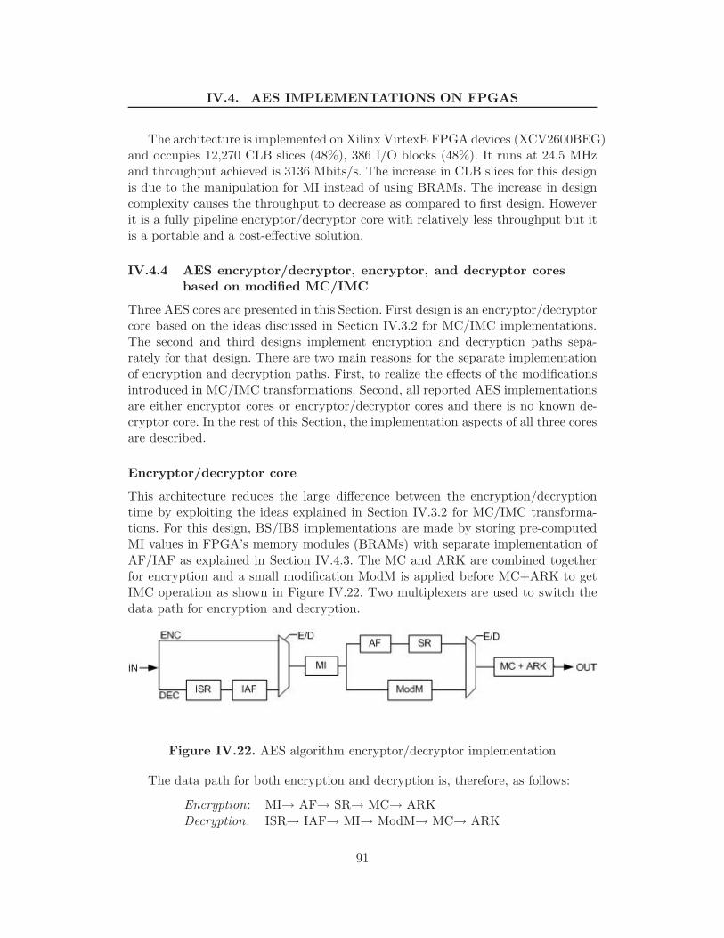
IV.4. AES IMPLEMENTATIONS ON FPGAS
The architecture is implemented on Xilinx VirtexE FPGA devices (XCV2600BEG)and occupies 12,270 CLB slices (48%), 386 I/O blocks (48%). It runs at 24.5 MHzand throughput achieved is 3136 Mbits/s. The increase in CLB slices for this designis due to the manipulation for MI instead of using BRAMs. The increase in designcomplexity causes the throughput to decrease as compared to first design. Howeverit is a fully pipeline encryptor/decryptor core with relatively less throughput but itis a portable and a cost-effective solution.
IV.4.4 AES encryptor/decryptor, encryptor, and decryptor coresbased on modified MC/IMC
Three AES cores are presented in this Section. First design is an encryptor/decryptorcore based on the ideas discussed in Section IV.3.2 for MC/IMC implementations.The second and third designs implement encryption and decryption paths sepa-rately for that design. There are two main reasons for the separate implementationof encryption and decryption paths. First, to realize the effects of the modificationsintroduced in MC/IMC transformations. Second, all reported AES implementationsare either encryptor cores or encryptor/decryptor cores and there is no known de-cryptor core. In the rest of this Section, the implementation aspects of all three coresare described.
Encryptor/decryptor core
This architecture reduces the large difference between the encryption/decryptiontime by exploiting the ideas explained in Section IV.3.2 for MC/IMC transforma-tions. For this design, BS/IBS implementations are made by storing pre-computedMI values in FPGA’s memory modules (BRAMs) with separate implementation ofAF/IAF as explained in Section IV.4.3. The MC and ARK are combined togetherfor encryption and a small modification ModM is applied before MC+ARK to getIMC operation as shown in Figure IV.22. Two multiplexers are used to switch thedata path for encryption and decryption.
Figure IV.22. AES algorithm encryptor/decryptor implementation
The data path for both encryption and decryption is, therefore, as follows:
Encryption: MI→ AF→ SR→ MC→ ARKDecryption: ISR→ IAF→ MI→ ModM→ MC→ ARK
91

IV. Architectural Designs For Advanced Encryption Standard
This AES encryptor/decryptor core occupies 80 BRAMs (43%), 386 I/O Blocks(48%) and 5677 slices (22.3%) by implementing on Xilinx VirtexE FPGA devices(XCV812BEG). It uses a system clock of 34.2 MHz and the data is processed at therate of 4121 Mbits/sec. This is a fully pipeline architecture optimized for both timeand space that performs at high speed and consumes less space. It is useful designfor applications where time factor dominates all other factors like cost, portabilityetc.
Encryptor core
It is a fully pipeline AES encryptor core. As it is already mentioned, the encryptorcore implements the encryption path for AES encryptor/decryptor core explained inthe last Section. The critical path for one encryption round is shown in Figure IV.23.
Figure IV.23. The data path for encryptor core implementation
For BS step, pre-computed values for S-Box are directly stored in the memories(BRAMs), therefore, AF transformation is embedded into BS. For symmetry pur-poses, BS and SR steps are combined together. Similarly MC and ARK steps aremerged to use 4-input/1-output CLB configuration which helps to decrement timedelays for the circuit. The encryption process starts from the first clock cycle as theround-keys are generated in parallel as described in Section IV.4.1. The encryptedblocks appear at the output after 11 clock cycles after the pipeline got filled. Oncethe pipeline is filled, the output is available at each consecutive clock cycle.
The encryptor core structure occupies 2136 CLB slices(22%), 100 BRAMs (35%)and 386 I/O blocks (95%) on targeting Xilinx VirtexE FPGA devices (XCV812BEG).It achieves a throughput of 5.2 Gbits/s at the rate of 40.575 MHz. A separate re-alization of this encryptor core provide a measure of timings for encryption processonly. The results shows huge boost in throughput by implementing the encryptorcore separately.
Decryptor Core
It is a fully pipeline decryptor core which implements the separate critical pathfor the AES encryptor/decryptor core explained in the same Section. The criticalpath for this decryptor core is taken from Figure IV.22 and then modified for IBSimplementations is shown in Figure IV.24.The computations for IBS step are made by using look-up tables and pre-computedvalues of inverse S-Box are directly stored in the memories (BRAMs). The IAF stepis embedded into IBS step for symmetric reasons which is obtained by just changingwires in FPGA implementations. The IMC step implementation is a major change inthis design, which is implemented by performing a small modification ModM before
92

IV.5. PERFORMANCE COMPARISON
Figure IV.24. The data path for decryptor core implementation
MC step as discussed in Section IV.3.2. The MC and ARK steps are merged for thesame reasons of targeting 4-input/1-output CLB structure.
The decryption process requires 11 cycles to generate the entire round Keys,then 11 cycles are consumed to fill the pipeline. Once the pipeline is filled theoutput plain-texts appear at the output after each consecutive clock cycle. On theother hand, decryptor core achieves a throughput of 4.95 Gbits/s at the rate of 38.67MHz by consuming 3216 CLB slices(34%), 100 BRAMs (35%) and 385 I/Os (95%).The implementation of decryptor core is made on Xilinx VirtexE FPGA devices(XCV812BEG).
By comparing encryptor and decryptor cores, there is no big difference in thenumber of CLB slices occupied by both encryptor and decryptor cores. Also theachieved throughput for both designs is very close. Both parameters indicate strongeffect by modified IMC transformation which resulted reduced data path for decryp-tion. The performance comparison of the separate implementations of encryptor anddecryptor cores with combined encryptor/decryptor implementation is significant.It provides another option to the end-user to select a big chip for combined imple-mentation or to choose two small chips for separate implementations of encryptorand decryptor cores to accomplish high gains in throughput.
IV.5 Performance comparison
IV.5.1 Previous work
Although the selection of new advanced encryption standard was finalized on Octo-ber, 2000, still very few AES implementations are reported on FPGAs. Three mainfeatures are observed for the previous AES implementations on FPGAs.
1. Algorithm’s selection: Not all of the AES architectures implemented thewhole process: encryption, decryption and key schedule algorithms. Most ofthem implement the encryption part only. The key schedule algorithm is of-ten ignored and it is supposed that keys are stored in the internal memory ofFPGAs or can be provided through an external interface. The FPGA’s imple-mentations at [33, 30, 25] are encryptor cores and the key schedule algorithmis implemented for the design at [25] only. The AES cores at [52, 10, 11]implements both encryption and decryption with key schedule algorithm.
2. Design’s strategy: This is an important factor that decides design’s strategyas area/time tradeoffs. The reported AES cores adopted various implemen-tation’s strategies. Some of them are iterative looping (IL) [33], sub-pipline
93

IV. Architectural Designs For Advanced Encryption Standard
(SP) [30], one-round implementation [25]. Few fully pipeline (PP) architec-tures have been also reported at [52, 10, 11].
3. Selection of FPGA: The high performance of AES cores is also subjected tothe selection of FPGAs. High performance FPGAs can be efficiently used toachieve high gains in throughput. Most of the reported AES cores used Virtexseries devices (XCV812, XCV1000, XCV3200). Those are single chip FPGAimplementations. Some AES cores achieved ultra high throughput but at thecost of multi-chip FPGA architectures [10, 11].
IV.5.2 Results comparison
The results comparison for FPGA’s implementations is not simple, since the threefeatures mentioned strongly affect the algorithm performance. It would be a faircomparison if it were done under the same environment for all implementations.The performance of an encryptor core must be compared with the performances ofthe encryptor cores using the same FPGA, same design’s strategies and same designspecifications. Table IV.3 provides a quick comparison of the results with existingFPGA implementations. The comparison of encryptor/decryptor cores is made firstfollowed by the comparison of encryptor cores with existing FPGA implementations.Finally, the comments are provided for our decryptor core implementation.
Our encryptor/decryptor cores (Sec. IV.4.3) are compared with the only knownencryptor/decryptor core architecture at [52]. The first encryptor/decryptor core(Sec. IV.4.3) improves design at [52] both in speed and area. There is an increase of15% in throughput at 15% less area utilization. The second encryptor/core (Sec.IV.4.3)is based on on-fly architecture scheme for BS/IBS computations in GF(24) andGF(22)2 and does not occupy BRAMs. In fact, memory requirements for the firstencryptor/decryptor core (Sec. IV.4.3) were overcomed by introducing this idea. Thepenalty paid was an increment in CLB slices however throughput still proves to becompetitive. Our encryptor/decryptor core (Sec. IV.4.4) is another highly optimizedcore. The results are highly appreciable as it requires up to 27.23% higher through-put, 25.06% less CLB slices and 21.56% less BRAMs than the fastest AES single-chipFPGA implementation at [52]. That high performance is obtained by reducing delayin the data paths for MC/IMC transformations, by using highly efficient memoriesBRAMs for BS/IBS computations, and by optimizing the circuit for long delays.It should be noted that some highly efficient AES encryptor/decryptor cores areavailable at [10, 11]. Those cores are for commercial use and high throughput isachieved by targeting multi-chip FPGA architectures.
According current results, our encryptor core design (Sec. IV.4.2) can be com-pared with two existing cores at [33, 25], since they are encryptor cores using thesame IL architecture. Those cores were implemented to compare performance re-sults for AES candidates algorithms and are designed to achieve high timing perfor-mances by using some primary assumptions. The design at [33] does not implementkey schedule and use external interfaces to load input data and to store output data,
94

IV.6. CONCLUSIONS
the feedback paths are not observed. The design at [25] implements key schedulealgorithm too and achieves high throughput by using 5673 CLB slices. Both imple-mentations are nice for comparing AES candidates and not for practical uses. How-ever, our encryptor core is optimized for both area/time parameters and includes acomplete set-up for encryption process. The user-key is accepted and round-keys aregenerated. The results of each round are latched for next rounds and a final outputappears at the output after 10 rounds. The design complexity therefore, increaseswhich causes the decrease in throughput however our encryptor occupies 2744 CLBslices, less CLB slices for any encryptor core reported to-date. Similarly, our fullypipeline encryptor cores (Sec. IV.4.2 and IV.4.4) well compare with the similar de-sign in [52]. Due to the optimization work for reducing design area, our fully pipelinearchitecture consumes only 2136 CLB slices plus 100 BRAMs. Throughput obtainedfor this architecture is 5.2 Gbits/s. The timing optimizations are pending and thereexist strong chances to improve throughput in the range of 6 to 7 Gbits/s.
Finally, our decryptor core (Sec. IV.4.4) achieves a throughput of 4.9 Gbits/sby consuming 3216 CLB slices. The author does not know any reported decryptorcore implementation on FPGAs for the purpose of comparison. Decryptor core im-plementation was considered important for our investigation work about AES toestimate performances for combined and separated implementations of the encryp-tor and decryptor cores. In addition, it is convenient to provide an option to theend-user for the selection of encryptor/decryptor core on a single chip or encryptorand decryptor cores on two small chips with high gains in throughput.
Table IV.3. Specifications of AES FPGA implementations.Core Type Device BRAMs CLB(S) Throughput T/S
(XCV) Slices Mbits/s (T)Gaj et al [33] E IL 1000 2902 331.5 0.11Dandalis et al [25] E IL 1000 5673 353 0.06Elbirt et al [30] E SP 1000 9004 1940 0.26McLoone et al [52] E P 812E 100 2222 6956 3.1McLoone et al [52] E/D P 3200E 102 7576 3239 0.43Sec. IV.4.3 [84] E/D P 2600E 80 6676 3840 0.58Sec. IV.4.3 [84] E/D P 2600E 13416 3136 0.24Sec. IV.4.4 [75] E/D P 2600E 100 5677 4121 1.73Sec. IV.4.2 [82] E IL 812E 2744 258.5 0.09Sec. IV.4.2 [82] E P 812E 100 2136 5193 2.43Sec. IV.4.4 [83] E P 812E 100 2136 5193 2.43Sec. IV.4.4 [80] D P 812E 100 3216 4949 1.54
IV.6 Conclusions
A variety of different encryptor, decryptor and encryptor/decryptor AES coresare presented. The encryptor cores are implemented both in iterative and pipeline
95

IV. Architectural Designs For Advanced Encryption Standard
modes. Some novel implementation techniques are presented for the implementationsof encryptor/decryptor cores which include: composite field approach for BS/IBS,look-up table method for BS/IBS, and modified MC/IMC approach. All the archi-tectures are highly optimized AES cores that tradeoff between time and area. Foreach architecture, we focus not only time performances but space is also a majorconcern. Three main factors were considered for implementing diverse AES cores.
• High performance : High performances require efficient usage of fast FPGA’sresources. Similarly efficient algorithmic techniques enhance design perfor-mance.
• Low cost solution : It refers to iterative architectures which occupy less hard-ware area at the cost of speed. Such architectures accommodate in smaller andconsequently low cost FPGAs.
• Portable architecture: A portable architecture can be migrated to most of theFPGAs by introducing minor modifications in the design. It provides an optionto the end-user to choose FPGA of his own choice. Portability can be achievedwhen a design targets to the standard resources available in most FPGAs. Ageneral methodology for achieving a portable architecture, in some cases, coststiming decrease in performance.
For AES encryptor cores, both iterative and fully pipeline architectures are im-plemented. The high timing performances are achieved by consuming the minimumspace occupied by any AES core reported to-date. The iterative encryptor coredesign is implemented using VirtexE device XCV812 by occupying the standardresources of the FPGAs and therefore can be migrated to all other family of FPGAdevices. The fully pipeline encryptor core is implemented on the same device (Vir-texE device XCV812). That core is optimized for high timing performances by usingdedicated memory resources (BRAMs); it is a fully pipeline architecture useful forthe applications where time is crucial and other factors like portability and cost are ofsecondary concern. The same factors can be considered to AES encryptor/decryptorcores. The AES encryptor/decryptor cores based on the BS/IBS implementationusing look-up table method are efficient architectures as compared to BS/IBS im-plementation using composite fields which is a portable and low cost solution. TheAES encryptor/decryptor core based on the modified MC/IMC is a good exampleto achieve high performance by using both efficient design and algorithmic tech-niques. It is a single-chip FPGA implementation that exhibits high performance atlow area consumption. In short, time/area tradeoffs are always present, however byusing efficient techniques at both design and algorithm level, the gap between areaand time can be significantly reduced. A fully pipeline decryptor core for FPGAswas presented and there is no other known decryptor core implementation reportedin the literature. FPGA implementations presented in this Section are competitiveor in some cases even outperforms existing FPGA implementations reported in theliterature to-date.
96

Chapter V
Elliptic Curve Cryptography
In this chapter we present a generic parallel architecture for the computation of thescalar multiplication over binary fields for two elliptic curve forms: and Weierstrassnon-singular form. The architecture was designed as general as possible trying tomake no assumptions about the specific hardware platform to be used by the de-signers. The idea of using parallel strategies was considered in every design stageand implemented as much as our hardware resources allowed us to do it so. The de-sign results reported in this work allow us to compute GF(2191) elliptic curve scalarmultiplication operations for the Hessian and the Weierstrass non-singular form inabout 114.7µ Secs and 59.26µ Secs, respectively.
V.1 Introduction
Over the past 17 years, many mathematical evidences have consistently shown thatElliptic Curve Cryptography (ECC) offers more security by key length than anyother major public key cryptosystem. The most important operation for ellipticcurve cryptosystems is the so-called Scalar multiplication operation. Let n be apositive integer and P a point on an elliptic curve. Then the scalar multiple Q = nPis the point resulting of adding n − 1 copies of P to itself. Scalar multiplication isthe main building block used in all the three fundamental ECC primitives: KeyGeneration, Signature and Verification schemes.
The security of elliptic curve systems is based on the intractability of the ellipticcurve discrete logarithm problem (ECDLP) that can be formulated as follows. Givenan elliptic curve E defined over a finite field Fq and two points Q and P that belongto the curve, where P has order r, find a positive scalar n ∈ [0, r − 1] such that theequation Q = nP holds. Solving the discrete logarithm problem over elliptic curvesis believed to be an extremely hard mathematical problem, much harder than itsanalogous one defined over finite fields of the same size.
97

V. A Generic Coprocessor For Elliptic Curve Scalar Multiplication onHardware
Figure V.1. Hierarchical Model for Elliptic Curve Cryptography
Several implementations have been reported so far [39, 92, 67, 91, 16, 89], andmost of them utilize a four-layer hierarchical scheme such as the one depicted inFigure V.1. As a consequence, high performance implementations of elliptic curvecryptography directly depend on the efficiency in the computation of the threeunderlying layers of the model.
The main idea discussed throughout this chapter is that each one of the threebottom layers shown in Figure V.1 can be implemented using parallel strategies.Although parallel architectures offer an interesting potential for obtaining a hightiming performance at the price of area, only in [91, 16] authors have explicitlyattempted a parallel strategy to compute elliptic curve scalar multiplication. Thecontribution of this Chapter is the design of a generic parallel architecture espe-cially tailored to obtain fast computation of the elliptic curves scalar multiplicationoperation. The architecture proposed here exploits the inherent parallelism of twoelliptic curves forms defined over GF(2m): The Hessian form and the Weierstrassnon-supersingular form.
The rest of this Chapter is organized as follows. Section V.2 explains GF (2m)finite field arithmetic. In Section V.3 we briefly describe the Hessian and WeierstrassForms of an elliptic curve together with their corresponding group laws. We alsoinclude some comments about the different design options that one can take inorder to obtain a parallel version of the point addition and doubling operators. InSection V.4 we describe the generic parallel architecture for scalar multiplicationthat constitutes the main contribution of this chapter. Then in Section V.5 we giveall the design details accomplished to implement the proposed architecture on anFPGA platform. Section V.6 includes a performance comparison of our design withother similar implementations previously reported. Finally, in Section V.7 someconclusions remarks as well as future work are drawn.
V.2 GF (2m) Finite field arithmetic
Arithmetic over GF (2m) has many important applications, in particular in the the-ory of error control coding and in cryptography [54, 57, 101]. Finite field’s arithmetic
98

V.2. GF (2M ) FINITE FIELD ARITHMETIC
operations include addition, subtraction, multiplication, and division. Addition andsubtraction are equivalent operations in GF (2m). Addition in binary finite fields isdefined as polynomial addition and can be implemented simply as the XOR additionof the two m-bit operands.
Let A(x), B(x) and C ′(x) ∈ GF (2m) and P (x) be the irreducible polynomialgenerating GF (2m). Multiplication in GF (2m) is defined as polynomial multiplica-tion modulo the irreducible polynomial P (x), C ′(x) = A(x)B(x) mod P (x). Inorder to obtain C ′(x), we can first obtain the product polynomial C(x) of degree atmost 2m− 2, as
C(x) = A(x)B(x) = (m−1∑i=0
aixi)(
m−1∑i=0
bixi) (V.1)
In a second step the reduction operation needs to be performed in order to obtainthe m− 1 degree polynomial C ′(x), which is defined as
C ′(x) = C(x) mod P (x) (V.2)
Notice that once the irreducible polynomial P (x) has been selected, the reductionstep can be accomplished by using XOR gates only.
Hardware implementation efficiency of finite field arithmetic is measured in termsof the associated space and time complexities. Space complexity is defined as thetotal amount of hardware resources needed to implement the circuit, whereas timecomplexity is the total delay of the circuit.
In the rest of this section different implementation aspects and several efficientmethods to compute GF (2m) finite field arithmetic are discussed. In § V.2.1 and§ V.2.2 we study the problem of how to compute Equation V.1 efficiently, consideringtwo separate cases. First, in section § V.2.1 a variation of the classical Karatsuba-Ofman algorithm is analyzed as one of the most efficient techniques to find thepolynomial product of Equation V.1. In subsection § V.2.2 we describe an efficientmethod to compute polynomial squaring in hardware, at a complexity cost of onlyO(1). In § V.2.3 we describe in detail a highly efficient hardware implementationthat carries on the reduction step of Equation V.2. Finally, in § V.2.4, it is explainedof how the inversion in GF (2m) can be computed in less number of clock cycles.
V.2.1 Binary Karatsuba-Ofman multipliers
Several architectures have been reported for multiplication in GF (2m). For example,efficient bit-parallel multipliers for both canonical and normal basis representationhave been proposed in [41, 95, 61, 104, 16]. All these algorithms exhibit a spacecomplexity O(m2). However, there are some asymptotically faster methods for fi-nite field multiplications, such as the Karatsuba-Ofman algorithm [70]. Discoveredin 1962, it was the first algorithm to accomplish polynomial multiplication in under
99

V. A Generic Coprocessor For Elliptic Curve Scalar Multiplication onHardware
O(m2) operations [15]. Karatsuba-Ofman multipliers may result in fewer bit opera-tions at the expense of some design restrictions, particularly in the selection of thedegree of the generating irreducible polynomial m.
In [37] was presented a Karatsuba multiplier based on composite fields of thetype GF ((2n)s) with m = sn, s = 2t, t an integer. However, for certain applica-tions, quite particularly, elliptic curve cryptosystems, it is important to considerfinite fields GF (2m) where m is not necessarily a power of two. In fact, for this spe-cific application some sources [68] suggest that, for security purposes, it is stronglyrecommended to choose degrees m primes for finite fields in the range [160, 512].
In the rest of this subsection we will briefly describe a variation of the classicKaratsuba-Ofman Multiplier called binary Karatsuba-Ofman multipliers that wasfirst presented in [74]. Binary Karatsuba-Ofman multipliers can be utilized arbitrar-ily, regardless the form of the required degree m.
Let the field GF (2m) be constructed using the irreducible polynomial P (x) ofdegree m = rn, with r = 2k, k an integer. Let A,B be two elements in GF (2m).Both elements can be represented in the polynomial basis as,
A =m−1∑i=0
aixi =
m−1∑i= m
2
aixi +
m2−1∑
i=0
aixi
= xm2
m2−1∑
i=0
ai+ m2xi +
m2−1∑
i=0
aixi = x
m2 AH + AL
and
B =m−1∑i=0
bixi =
m−1∑i= m
2
bixi +
m2−1∑
i=0
bixi
= xm2
m2−1∑
i=0
bi+ m2xi +
m2−1∑
i=0
bixi = x
m2 BH + BL.
Then, using last two equations, the polynomial product is given as
C = xmAHBH + (AHBL + ALBH)xm2 + ALBL. (V.3)
Karatsuba-Ofman algorithm is based on the idea that the product of last equationcan be equivalently written as,
C = xmAHBH + ALBL+(AHBH + ALBL + (AH + AL)(BL + BH))x
m2
= xmCH + CL.
(V.4)
Let us define
MA := AH + AL;MB := BL + BH ;M := MAMB .
(V.5)
100

V.2. GF (2M ) FINITE FIELD ARITHMETIC
Using Equation V.4, and taking into account that the polynomial product C has atmost 2m− 1 coordinates, we can classify its coordinates as,
CH = [c2m−2, c2m−3, . . . , cm+1, cm];CL = [cm−1, cm−2, . . . , c1, c0].
(V.6)
Although (V.4) seems to be more complicated than (V.3), it is easy to see thatEquation (V.4) can be used to compute the product at a cost of four polynomialadditions and three polynomial multiplications. In contrast, when using equation(V.3), one needs to compute four polynomial multiplications and three polynomialadditions. Due to the fact that polynomial multiplications are in general much moreexpensive operations than polynomial additions, it is valid to conclude that (V.4) iscomputationally simpler than the classic algorithm.
Input: Two elements A, B ∈ GF (2m) with m = rn = 2kn, and
where A, B can be expressed as,
A = xm2 AH + AL, B = x
m2 BH + BL.
Output: A polynomial C = AB with up to 2m − 1 coordinates,
where C = xmCH + CL.
Procedure Kmul2k(C, A, B)
0. begin
1. if (r == 1) then
2. C = mul n(A, B);
3. return;
4. for i from 0 to r2− 1 do
5. MAi = ALi + AH
i ;
6. MBi = BLi + BH
i ;
7. end
8. mul2k(CL, AL, BL);
9. mul2k(M, MA, MB);
10. mul2k(CH , AH , BH);
11. for i from 0 to r − 1 do
12. Mi = Mi + CLi + CH
i ;
13. end
14. for i from 0 to r − 1 do
15. C r2+i = C r
2+i + Mi;
16. end
17. end
Figure V.2. m = 2kn-bit Karatsuba-Ofman multiplier.
Karatsuba-Ofman’s algorithm can be applied recursively to the three polynomialmultiplications in (V.4). Hence, we can postpone the computations of the polynomialproducts AHBH , ALBL and M , and instead we can split again each one of thesethree factors into three polynomial products. By applying this strategy recursively,
101

V. A Generic Coprocessor For Elliptic Curve Scalar Multiplication onHardware
in each iteration each degree polynomial multiplication is transformed into threepolynomial multiplications with their degrees reduced to about half of its previousvalue.
Eventually, after no more than �log2(m)� iterations, all the polynomial operandscollapse into single coefficients. In the last iteration, the resulting bit multiplicationscan be directly computed. Although it is possible to implement the Karatsuba-Ofman algorithm until the �log2 m� iteration, it is usually more practical to truncatethe algorithm earlier. If the Karatsuba-Ofman algorithm is truncated at a certainpoint, the remaining multiplications can be computed by using alternative tech-niques (classic algorithm or other techniques).
The algorithm presented in Figure V.2 implements the Karatsuba-Ofman strat-egy for polynomial multiplication. By Combining the Karatsuba-Ofman algorithmwith the classic algorithm, it can be shown [74] that the space and time complexitiesof the hybrid m-bit Karatsuba-Ofman multiplier truncated at the n-bit multiplicandlevel are upper bounded by
# XORs ≤ (mn
)log2 3 (n2 + 6n− 1)− 8m + 2 ;
# ANDs ≤ 3log2 rMand2n =(
mn
)log2 3n2; (V.7)
Delay ≤ TAND + TX(log2 n + 4 log2 r) .
Where TX and TAND correspond to an XOR gate delay and an AND gate delay,respectively. Table V.1 shows the space and time complexities of Karatsuba-Ofmanmultipliers for the optimal case when m is a power of two. The values of m presentedin Table V.1 are the first eight powers of two. Various factors including target devicesand design techniques influence the space complexity in terms of number of CLBs.The space complexity provided in the last column of Table V.1 is based on ourexperimental results optimized for VirtexE devices only.
Table V.1. Space and time complexities for several m = 2k-bit hybrid Karatsuba-Ofman multipliers.
m r n AND gates XOR gates Time delay Area (in CLBs)1 1 1 1 0 TA −2 1 2 4 1 TX + TA −4 1 4 16 9 2TX + TA 88 2 4 48 55 6TX + TA 3216 4 4 144 225 10TX + TA 11532 8 4 432 799 14TX + TA 36864 16 4 1296 2649 18TX + TA 1171128 32 4 3888 8455 22TX + TA 3379
To generalize the Karatsuba-Ofman algorithm of Figure V.2 for arbitrary degreesm, particularly m primes, let us consider the multiplication of two polynomialsA,B ∈ GF (2m), such that their degree is less or equal to m− 1, where m = 2k + d.As a very first approach, we could pretend that both operands have 2k+1 coordinates
102

V.2. GF (2M ) FINITE FIELD ARITHMETIC
A = [2k+1−d︷ ︸︸ ︷
0, . . . , 0, 0, a2k+d−1, . . . , a2k+1, a2k︸ ︷︷ ︸AH
,
AL︷ ︸︸ ︷a2k−1, a2k−2, . . . , a2, a1, a0];
AH = [0, . . . , 0, 0, a2k+d−1, . . . , a2k+1, a2k ];AL = [a2k−1, a2k−2, . . . , a2, a1, a0];
Figure V.3. Binary Karatsuba-Ofman strategy
each, where their respective 2k+1−d most significant bits are all equal to zero. FigureV.3 shows how the subpolynomials AH and AL will be redefined according with thisapproach. If we partition the operands A and B as shown in Figure V.3, then, inorder to compute their polynomial multiplication, we can use the regular Karatsuba-Ofman algorithm using m = 2k+1. Although this approach is a valid one, it clearlyimplies the waste of several arithmetic operations, as some of the most significant bitsof the operands are zeroes. However, if we were able to identify the extra arithmeticoperations and remove them from the computation, we would then be able to finda quasi-optimal solution for arbitrary degrees of m. To see how this can be done,consider the algorithm shown in Figure V.4, which has been adapted from the onepresented in previous Figure V.2.
In lines 1-2 the values of the constants k, d such that m = 2k + d are computed.If d = 0, i.e, if m is a power of two, then the binary Karatsuba-Ofman algorithm ofFigure V.4 reverts to the specialized algorithm in Figure V.2 presented in the pre-vious section. If that is not the case, the algorithm of Figure V.4 uses the constantsk and d to prevent us to compute unnecessary arithmetic operations. In lines 6-9,the d least significant bits of MA and MB of equation (V.5) are computed usingthe d non-zero coordinates of AH and BH . The remaining k − d most significantbits of MA and MB are directly obtained from AL and BL, respectively. Noticethat the operands, AL, BL,MA and MB are all 2k-bit polynomials. Because of that,our algorithm invokes the multiplier of Figure V.2 in lines 10 and 11. On the otherhand, both operands AH and BH are d-bit polynomials, where d, in general, is nota power of two. Consequently, in line 12, the algorithm calls itself in a recursivemanner. This recursive call is invoked using the operand’s degree reduced to d. Ineach iteration the degree of the operands gets reduced, and eventually, after a totalof h iterations (where h is the hamming weight of the binary representation of theoriginal degree m), the algorithm ends. As a design example, consider the binaryKaratsuba-Ofman multiplier shown in Figure V.5. That circuit computes the poly-nomial multiplication of the elements A and B ∈ GF (2191). Notice that for thiscase m = 191 = 2k + d = 27 + 63. Since (191)2 = 10111111, the Hammingweight h of the binary representation of m is h = 7. This implies that we wouldneed a total of seven iterations in order to compute the multiplication using the
103

V. A Generic Coprocessor For Elliptic Curve Scalar Multiplication onHardware
Input: Two elements A, B ∈ GF (2m) with m an arbitrary
number, and where A, B can be expressed as
A = xm2 AH + AL, B = x
m2 BH + BL.
Output: A polynomial C = AB with up to 2m − 1 coordinates,
where C = xmCH + CL.
Procedure mulgen m(C, A, B)
0. begin
1. k = �log2 m�;2. d = m − 2k;
3. if (d == 0) then
4. C = Kmul2k(A, B);
5. return;
6. for i from 0 to d − 1 do
7. MAi = ALi + AH
i ;
8. MBi = BLi + BH
i ;
9. end
10. mul2k(CL, AL, BL);
11. mul2k(M, MA, MB);
12. mulgen d(CH , AH , BH);
13. for i from 0 to 2k − 2 do
14. Mi = Mi + CLi + CH
i ;
15. end
16. for i from 0 to 2k − 2 do
17. Ck+i = Ck+i + Mi;
18. end
19. end
Figure V.4. m-bit binary Karatsuba-Ofman multiplier.
Figure V.5. Karatsuba Multiplier GF (2191)
generalized m-bit binary Karatsuba-Ofman multiplier. However we can do muchbetter by assuming that the d = 63 most significant leftover bits are 64 (implying
104
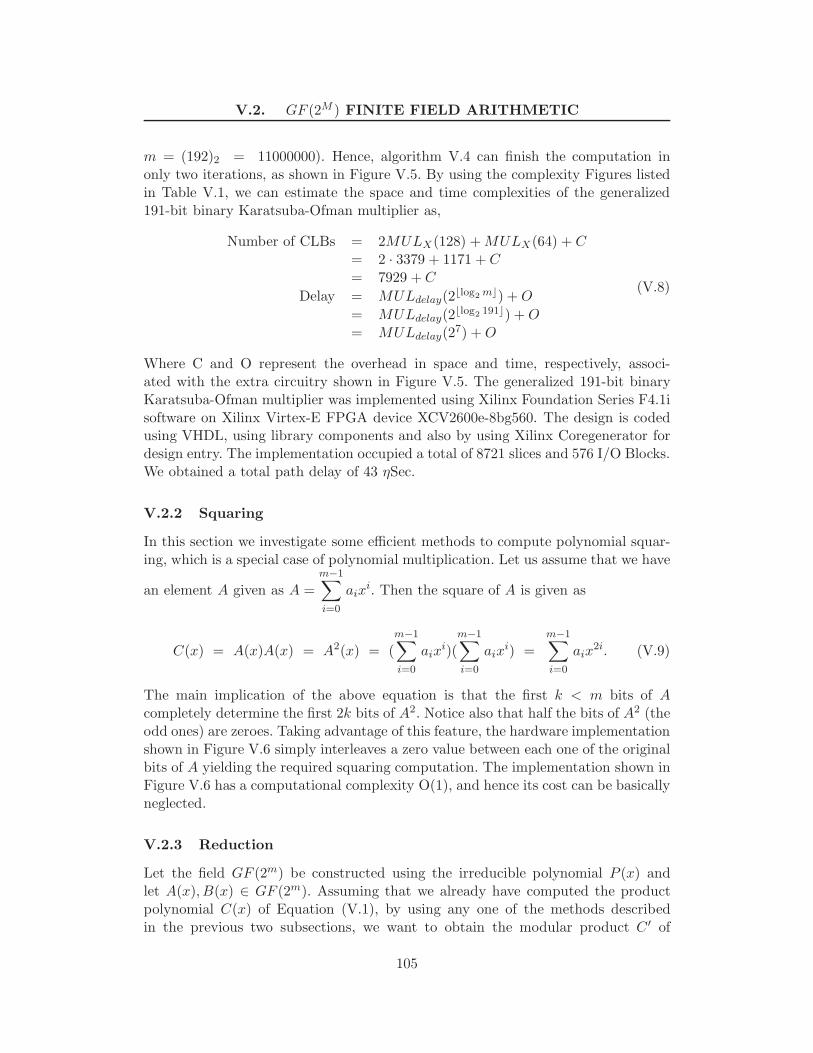
V.2. GF (2M ) FINITE FIELD ARITHMETIC
m = (192)2 = 11000000). Hence, algorithm V.4 can finish the computation inonly two iterations, as shown in Figure V.5. By using the complexity Figures listedin Table V.1, we can estimate the space and time complexities of the generalized191-bit binary Karatsuba-Ofman multiplier as,
Number of CLBs = 2MULX(128) + MULX(64) + C= 2 · 3379 + 1171 + C= 7929 + C
Delay = MULdelay(2�log2 m�) + O
= MULdelay(2�log2 191�) + O= MULdelay(27) + O
(V.8)
Where C and O represent the overhead in space and time, respectively, associ-ated with the extra circuitry shown in Figure V.5. The generalized 191-bit binaryKaratsuba-Ofman multiplier was implemented using Xilinx Foundation Series F4.1isoftware on Xilinx Virtex-E FPGA device XCV2600e-8bg560. The design is codedusing VHDL, using library components and also by using Xilinx Coregenerator fordesign entry. The implementation occupied a total of 8721 slices and 576 I/O Blocks.We obtained a total path delay of 43 ηSec.
V.2.2 Squaring
In this section we investigate some efficient methods to compute polynomial squar-ing, which is a special case of polynomial multiplication. Let us assume that we have
an element A given as A =m−1∑i=0
aixi. Then the square of A is given as
C(x) = A(x)A(x) = A2(x) = (m−1∑i=0
aixi)(
m−1∑i=0
aixi) =
m−1∑i=0
aix2i. (V.9)
The main implication of the above equation is that the first k < m bits of Acompletely determine the first 2k bits of A2. Notice also that half the bits of A2 (theodd ones) are zeroes. Taking advantage of this feature, the hardware implementationshown in Figure V.6 simply interleaves a zero value between each one of the originalbits of A yielding the required squaring computation. The implementation shown inFigure V.6 has a computational complexity O(1), and hence its cost can be basicallyneglected.
V.2.3 Reduction
Let the field GF (2m) be constructed using the irreducible polynomial P (x) andlet A(x), B(x) ∈ GF (2m). Assuming that we already have computed the productpolynomial C(x) of Equation (V.1), by using any one of the methods describedin the previous two subsections, we want to obtain the modular product C ′ of
105

V. A Generic Coprocessor For Elliptic Curve Scalar Multiplication onHardware
Figure V.6. Squaring Circuit
Equation (V.2). Recall that the polynomial product C and the modular product C ′,have 2m− 1 and m, coordinates, respectively, i.e.,
C = [c2m−2, c2m−3, . . . , cm+1, cm, . . . , c1, c0];C ′ = [c′m−1, c
′m−2, . . . , c′1, c′0].
(V.10)
Once the generating polynomial P (x) has been selected, the reduction step thatobtains C ′ from C can be computed by using XOR and shift operations only. Letthe field GF (2m) be constructed using the irreducible trinomial P (x) = xm +xn +1with a root α and 1 < n < m
2 . Let also A(x), B(x) be elements in GF (2m). In orderto obtain the modular product C ′(x) of (V.1), we use the property P (α) = 0, andwrite
αm = 1 + αn ;αm+1 = α + αn+1 ;
...α2m−3 = αm−3 + αm+n−3 ;α2m−2 = αm−2 + αm+n−2 .
(V.11)
The above m − 1 set of identities suggests a method to obtain the m-coordinatesof the modular product C ′ of Equation (V.2). We can partially reduce the 2m − 1coordinates of C by reducing its most significant m− 1 bits into its first m + n− 1bits, as indicated by (V.11). For instance, in order to obtain the first partiallyreduced coordinate c′0 we just need to add the regular product coordinate cm to thec0 coordinate, yielding c′0 as c′0 = c0 + cm.
Similarly the whole set of m + n− 2 partially reduced coordinates can be found
106

V.2. GF (2M ) FINITE FIELD ARITHMETIC
as,
c′0 = c0 + cm ;c′1 = c1 + cm+1 ;
...c′n−1 = cn−1 + cm+n−1 ;c′n = cn + cm+n + cm ;c′n+1 = cn+1 + cm+n+1 + cm+1 ;
...c′m−2 = cm−2 + c2m−2 + c2m−n−2 ;c′m−1 = cm−1 + c2m−n−1 ;c′m = cm + c2m−n ;
...c′m+n−3 = cm+n−3 + c2m−3 ;c′m+n−2 = cm+n−2 + c2m−2 .
(V.12)
Notice that in the reduction process of (V.12), the constant coefficient of the irre-ducible generating trinomial P (x) reflects its influence in the first m − 1 partiallyreduced bits. The middle term of P (x), on the other hand, affects the partially re-duced bits of (V.12) in the range [c′n, c′m+n−2]. Notice also that there is an overlap
Figure V.7. Reduction Diagram
in the range [c′n, c′m−2], where both the constant and the middle coefficients of P (x)affect the partially reduced coordinates.
We say that the coefficients in (V.12) have been partially reduced because ingeneral, if n > 1, we still need to reduce the n−2 most significant reduced coordinates
107
V. A Generic Coprocessor For Elliptic Curve Scalar Multiplication onHardware
of (V.12). However, this same idea can be used repeatedly until the m− 1 modularcoordinates of (V.10) are obtained. Each time that this strategy is applied we reducem− n coordinates.
Figure V.7 shows how to implement on reconfigurable hardware the reductionstrategy just outlined. As it was mentioned before, the reduction step involves XORand overlap operations only.
Although the strategy shown in Figure V.7 works for arbitrary irreducible trino-mials, for the purposes of this research work we utilized a fixed irreducible generatingtrinomial, namely, P (x) = x191 + x9 + 1.
V.2.4 Inversion
The Euclidean algorithm required O(n2) bit operations to perform inversion. Fermat’s Little Theorem (FLT) establishes that for any nonzero element α ∈ GF (2m), theidentity α−1 ≡ α2m−2 holds. Therefore, multiplicative inversion can be performedby computing,
α2m−2 = α21 × α21 × · · ·α2m−1(V.13)
A straightforward implementation of Eq. V.13 can be carried out using the binaryexponentiation method, which requires m−1 field squarings and m−2 field multipli-cations. The Itoh-Tsujii Multiplicative Inverse Algorithm (ITMIA) algorithm [44] onthe other hand, reduces the required number of multiplications to k+hw(m−1)−2,where k = log2(m− 1)� and hw(m − 1) are the number of bits and the Ham-ming weight of the binary representation of m − 1, respectively. This remarkablysaving on the number of multiplications is based on the observation that since2m − 2 = (2m−1 − 1) · 2, then the identity from Fermat’s little theorem can berewritten as α−1 ≡ α2m−2 ≡ α(2m−1−1)2 . Then ITMIA computes the field element(2m−1 − 1) using a recursive re-arrangement of the finite field operations.
Using the ITMIA algorithm one can find an addition chain for an arbitrarym. We used this algorithm to obtain an addition chain for m = 191 (our designexample). In this case e = m− 1 = 190 = 27 + 25 + 24 + 23 + 22 + 21. Therefore,
U = 1→ 2→ 4→ 8→ 16→ 32→ 64→ 128→160→ 176→ 184→ 188→ 190 (V.14)
The addition chain in Eq. V.14 can be accomplished using 12 multiplicationsand m − 1 squarings in accordance to the algorithm. However it can be seen thatvarious addition chains of shortest length for the same m exist. Let l be the shortestlength of any valid addition chain for a given positive integer e = m− 1. Then theproblem of finding an addition chain for e with length l is an NP-hard problem [58].Let us first formally define an addition chain in order to describe a methodology toachieve field multiplicative inverses.
108

V.2. GF (2M ) FINITE FIELD ARITHMETIC
Addition Chains
An addition chain U for a positive integer e = m − 1 of length t is a sequenceof positive integers U = {u0, u1, · · · , ut}, and an associated sequence of r pairsV = {(v1, v2 · · · , vt} with vi = (i1, i2), 0 ≤ i2 ≤ i1 < i, such that:
• u0 = 1 and ut = m− 1;
• for each ui, 1 ≤ i ≤ t, ui = ui1 + ui2 .
Consider the same design example for m = 191, e = m− 1 = 190− 1. Then, oneof possible addition chain with length t = 10 is,
U = 1→ 2→ 3→ 5→ 10→ 20→ 40→80→ 160→ 180→ 190 (V.15)
Each term of this chain ui is obtained either by doubling the immediate precedingterm ui−1 +ui−1 or by adding any two previous terms uj +uk. That provides us twoindices i1 and i2. In the former case, the same term was doubled so i1 = i2 = i− 1while for later case two different terms uj and uk were added provided i1 = j andi2 = k.
Input: An element α ∈ GF (2m), an addition chain U oflength t for m− 1 and its associated sequence V.Output: α−1 ∈ GF (2m)Procedure MultiplicativeInversion(α, U)1. β0 = α2. for i from 1 to t do:3. βi = (βi1)
2ui2 · βi2
4. return (βt2);
Figure V.8. An Algorithm for multiplicative inversion using addition chains
Consider the algorithm shown in Fig. V.8. That algorithm iteratively computesthe βi coefficients in the exact order stipulated by the addition chain U . Indeed,starting from β0 = (α)2
u0−1 = (α)2u0−1 = α21−1, the algorithm computes the
other t βi coefficients. In the final iteration, after having computed the coefficientβt = (α)2
m−1−1, the algorithm returns the required multiplicative inversion byperforming a regular field squaring, namely, β2
t = (α2m−2) = α−1.Let us assume that the binary extension field GF (2191) has been generated with
the trinomial P (x) = x191 + x9 + 1, irreducible over GF (2). Let α ∈ GF (2191) bean arbitrary nonzero field element. Then, using the addition chain of Example V.15,the algorithm of Fig. V.8 will compute the sequence of β coefficients as shown in
109

V. A Generic Coprocessor For Elliptic Curve Scalar Multiplication onHardware
Table V.2. Algorithm of Fig. V.8: βi Coefficient Generation
i ui i1 i2 ui2 rule β2ui2
i1· βi2 βi = α2u
i −1
0 1 0 0 1 – – β0 = α21−1
1 2 0 0 1 u0 + u0 β21
0 · β0 β1 = α22−1
2 3 1 0 1 u1 + u0 β21
1 · β0 β2 = α23−1
3 5 2 1 2 u2 + u1 β22
2 · β1 β3 = α25−1
4 10 3 3 5 u3 + u3 β25
3 · β3 β4 = α210−1
5 20 4 4 10 u4 + u4 β210
4 · β4 β5 = α220−1
6 40 5 5 20 u5 + u5 β220
5 · β5 β6 = α240−1
7 80 6 6 40 u6 + u6 β240
6 · β6 β7 = α280−1
8 160 7 7 80 u7 + u7 β280
7 · β7 β8 = α2160−1
9 180 8 5 20 u8 + u5 β220
8 · β5 β9 = α2180−1
10 190 9 4 10 u9 + u4 β210
9 · β4 β10 = α2190−1
Table V.2.4. Once again, notice that after having computed the coefficient β10 theonly remaining step is to obtain α−1 as, α−1 = β2
10
Let us now assess the computational complexity of the algorithm shown inFig. V.8. The algorithm performs t iterations (where t is the length of the addi-tion chain U) and one field multiplication per iteration. Thus, we conclude that atotal of t field multiplication computations are required.
On the other hand, notice that at each iteration i, a total of 2ui2 field squaringsare performed. Notice also that by definition, the addition chain guarantees that foreach ui, 1 ≤ i ≤ t, the relation ui2 = ui − ui1 holds. Hence, one can show byinduction that the total number of field squaring operations performed right afterthe execution of the i-esime iteration is ui− 1 [98]. Therefore, at the end of the finaliteration t, a total of ut − 1 = m − 2 squaring operations have been performed.This, together with the final squaring operation, yield a total of m−1 field squaringcomputations.
Summarizing, the algorithm of Fig. V.8 can find the inverse of any nonzeroelement of the field using exactly,
#Multiplications = t;#Squarings = m− 1. (V.16)
Squarer and Multiplier are the two main building blocks for performing inver-sion in GF(2m). We have already discussed the structure of our multiplier in Sec-tion V.2.1. Squaring in GF(2m) is a simple operation however, as it was stated inEq. V.16, it devours m−1 clock cycles performing m−1 squarings for m-bit inversion.However, much less field multiplications are needed for computing the multiplicative
110

V.3. ELLIPTIC CURVE SCALAR MULTIPLICATION
inversion, which is valuable for the design since field multiplication in GF(2m) is acostly and extensive time consuming operation. Figure V.9.a shows our strategy for
Figure V.9. Squarer GF(2193) (a) for x21(b) for x2n
implementation
implementing field squaring trying to use as few clock cycles as possible. Polynomialsquaring is free of cost and is obtained by connecting each alternate even bit to zero(ground). That operation is followed by a second step where reduction is performedby using few XOR gates. Figure V.9.b shows the GF (2191) field squarer implemen-tation used in this work. Referring to the addition chain described in Table V.2.4,frequent squaring operations in GF (2191) are βi
21(2 times), βi22 (1 time), βi25 (1
time), and βi210 (10 times).That is why we preferred to cascade 10 field squarer blocks back to back and
then by the appropriate use of multiplexers obtain the corresponding outputs after1, 2, 5, and 10 squarer blocks as shown in Figure V.9.b. As an example, the x220
field operation can be performed in just two clock cycles by taking the output afterthe last squarer block (10 squarers) in the first clock cycle and then after a secondclock cycle we will get the required 20 field squarings.
V.3 Elliptic curve scalar multiplication
In this section we discuss the Hessian form of elliptic curves and its group lawfollowed by Montgomery point multiplication algorithm. The group law for Mont-gomery point multiplication is discussed both in affine and projective coordinates.The discussions are also made for the conversion from projective to affine coordi-nates.
V.3.1 Hessian form
Let P (x) be a degree-m polynomial, irreducible over GF(2). Then P (x) generatesthe finite field Fq = GF (2m) of characteristic two. A Hessian elliptic curve E(Fq)is defined to be the set of points (x, y, z) ∈ GF (2m) × GF (2m) that satisfy thecanonical homogeneous equation,
x3 + y3 + z3 = Dxyz (V.17)
111

V. A Generic Coprocessor For Elliptic Curve Scalar Multiplication onHardware
Together with the point at infinity denoted by O and given by (1, 0,−1).The original form of the group law on curves in Hessian form belongs to Cauchy
and was later simplified by Sylvester-Desboves [23].Let P = (x1, y1, z1) and Q = (x2, y2, z2) be two points that belong to the plane
cubic curve of Eq. V.22. Then we define −P = (y1, x1, z1) and P + Q = (x3, y3, z3)where,
x3 = y12x2z2 − y2
2x1z1
y3 = x12y2z2 − x2
2y1z1
z3 = z12y2x2 − z2
2y1x1
(V.18)
Provided that P �= Q. The addition formulae of Eq. (V.18) might be parallelizedusing 12 field multiplications as follows [91],
λ1 = y1x2 λ2 = x1y2 λ3 = x1z2
λ4 = z1x2 λ5 = z1y2 λ6 = z2y1
s1 = λ1λ6 s2 = λ2λ3 s3 = λ5λ4
t1 = λ2λ5 t2 = λ1λ4 t3 = λ6λ3
x3 = s1 − t1 y3 = s2 − t2 z3 = s3 − t3
(V.19)
Whereas the formulae for point doubling are giving by
x3 = y1
(z1
3 − x13);
y3 = x1
(y1
3 − z13);
z3 = z1
(x1
3 − y13).
(V.20)
Where 2P = (x3, y3, z3). The doubling formulae of Eq. (V.20) can be also parallelizedrequiring 6 field multiplications plus three field squarings for their computation. Theresulting arrangement can be rewritten as [91],
λ1 = x12 λ2 = y1
2 λ3 = z12;
λ4 = x1λ1 λ5 = y1λ2 λ6 = z1λ3;λ7 = λ5 − λ6 λ8 = λ6 − λ4 λ9 = λ4 − λ5;x2 = y1λ8 y2 = x1λ7 z2 = z1λ9;
(V.21)
By implementing Eqs. (V.19) and (V.21), one can obtain the two building blocksneeded for the implementation of the second layer shown in Figure V.1. Hence,provided that those two blocks are available, one can compute the third layer ofFigure V.1 by using the well-known doubling and add algorithm of Figure V.10.That sequential algorithm needs an average of m
2 point additions plus m pointdoublings in order to complete one scalar multiplication computation.
Alternatively, we can use the algorithm of Figure V.11 that can potentially beimplemented in parallel since in this case the point addition and doubling operationsdo not show any dependencies between them. Therefore, if we assume that thealgorithm of Figure V.11 is implemented in parallel, one needs an average of just m
2point additions plus m
2 point doublings in order to complete one scalar multiplicationcomputation.
In Subsection V.3.3 we discuss how to obtain an efficient parallel-sequentialimplementation of the second and third layers of the model of Figure V.1.
112

V.3. ELLIPTIC CURVE SCALAR MULTIPLICATION
Input: k = (kn−1, kn−2....., k1, k0)2 with kn−1 = 1,P (x, y, z) ∈ E(F2m)Output: Q = kP
1. Set Q = P
2. For i from n− 2 downto 0 do3. Q = 2.Q (point doubling)4. if (ki = 1) then5. Q = Q + P (point addition)6. end if;7. end for;
Figure V.10. Doubling & Add algorithm for Scalar Multiplication: MSB-First
Input: k = (kn−1, kn−2....., k1, k0)2 with kn−1 = 1,P (x, y, z) ∈ E(F2m)Output: Q = kP
1. Set Q = 1; R = P
2. For i from 0 to n− 1 do3. if (ki = 1) then4. Q = Q + R (point addition)5. R = 2.R (point doubling)6. end if;7. end for;
Figure V.11. Doubling & Add algorithm for Scalar Multiplication: LSB-First
V.3.2 Weierstrass Non-Singular form and Montgomery PointMultiplication Algorithm
Let P (x) be a degree-m polynomial, irreducible over GF (2). Then P (x) generatesthe finite field Fq = GF (2m) of characteristic two. A non-supersingular elliptic curveE(Fq) is defined to be the set of points (x, y) ∈ GF (2m)× GF (2m) that satisfy theaffine equation,
y2 + xy = x3 + ax2 + b, (V.22)
Where a and b ∈ Fq, b �= 0, together with the point at infinity denoted by O. Theelliptic curve group law in affine coordinates is given by:
Let P = (x1, y1) and Q = (x2, y2) be two points that belong to the curve V.22then −P = (x1, x1 + y1). For all P on the curve P + O = O + P = P . If Q �= −P ,
113

V. A Generic Coprocessor For Elliptic Curve Scalar Multiplication onHardware
then P + Q = (x3, y3), where
x3 =
{( y1+y2
x1+x2)2 + y1+y2
x1+x2+ x1 + x2 + a P �= Q
x21 + b
x21
P = Q (V.23)
y3 ={
( y1+y2
x1+x2)(x1 + x3) + x3 + y1 P �= Q
x21 + (x1 + y1
x1)x3 + x3 P = Q
(V.24)
It can be seen from Eqns. V.23 and V.24 that for both of them, point addition(when P �= −Q) and point doubling (when P = Q), the computations for (x3, y3)require one field inversion and two field multiplications neglecting the costs of fieldadditions and squarings. An important observation first made by Montgomery isthat the x-coordinate of 2P does not involve the y-coordinate of P .
I. Projective Coordinates
Compared with field multiplication in affine coordinates, inversion is by far themost expensive basic arithmetic operation in GF (2m). Inversion can be avoided bymeans of projective coordinate representation. A point P in projective coordinatesis represented using three coordinates X, Y, and Z. This representation greatly helpsto reduce internal computational operations. It is customary to convert the point Pback from projective to affine coordinates in the final step. This is due to the factthat affine coordinate representation involves the usage of only two coordinates andtherefore is more useful for external communication saving some valuable bandwidth.
In standard projective coordinates the projective point (X:Y:Z) with Z�= 0 cor-responds to the affine coordinates x = X/Z and y = Y/Z. The projective equationof the elliptic curve is given as:
Y 2Z + XY Z = X3 + aX2Z + bZ3 (V.25)
II. Montgomery Group Law
Let P = (x1, y1) and Q = (x2, y2) be two points that belong to the curve of Equa-tion V.22. Then P + Q = (x3, y3) and P − Q = (x4, y4), also belong to the curveand it can be shown that x3 is given as [39],
x3 = x4 +x1
x1 + x2+
(x1
x1 + x2
)2
; (V.26)
Hence we only need the x coordinates of P , Q and P − Q to exactly determinethe value of the x-coordinate of the point P + Q. Let the x coordinate of P berepresented by X/Z. Then, when the point 2P = (X2P , Y2P , Z2P ) is converted toprojective coordinate representation, it becomes [50],
x2P = X4 + b · Z4;z2P = X2 · Z2;
(V.27)
114

V.3. ELLIPTIC CURVE SCALAR MULTIPLICATION
The computation of Eq. V.27 requires one general multiplication, one multiplica-tion by the constant b, five squarings and one addition. Fig. V.12 is the sequence ofinstructions needed to compute a single point doubling operation Mdouble(X1, Z1)efficiently.
Input: P = (X1,−, Z1) ∈ E(F2m), c such that c2 = b
Output: P = 2 · PProcedure: Mdouble(X1, Z1)
1. T = X21
2. M = c · Z21
3. Z1 = T · Z21
4. M = M2
5. T = T 2
6. X1 = T + M
Figure V.12. Montgomery point doubling
In a similar way, the coordinates of P + Q in projective coordinates can becomputed as the fraction X3/Z3 and are given as:
Z3 = (X1 · Z2 + X2 · Z1)2 ;
X3 = x · Z3 + (X1 · Z2) · (X2 · Z1);(V.28)
Input: P = (X1,−, Z1), Q = (X2,−, Z2) ∈ E(F2m)Output: P = P + Q
Procedure: Madd(X1, Z1, X2, Z2)
1. M = (X1 · Z2) + (Z1 ·X2)2. Z1 = M2
3. N = (X1 · Z2) · (Z1 ·X2)4. M = x · Z3
5. X1 = M + N
Figure V.13. Montgomery point addition
The required field operations for point addition of Eq. V.28 are three generalmultiplications, one multiplication by x, one squaring and two additions. This op-eration can be efficiently implemented as shown in Fig. V.13.
115

V. A Generic Coprocessor For Elliptic Curve Scalar Multiplication onHardware
III. Montgomery Point Multiplication
A method based on the formulas for doubling (from Eq. V.27) and for addition(from Eq. V.28) is shown in Fig. V.14 [50]. Notice that steps 2.2 and 2.3 areformulae for point doubling (Mdouble) and point addition (Madd) from Figs. V.12and V.13 respectively. In fact both Mdouble and Madd operations are executed ineach iteration of the algorithm. If the test bit ki is ‘1’, the manipulations are madefor Madd(X1, Z1,X2, Z2) and Mdouble(X2, Z2) (step 2.2) else Madd(X2, Z2,X1, Z1)and Mdouble(X1, Z1) i-e Mdouble and Madd with reversed arguments (step 2.3).
The approximate running time of the algorithm shown in Fig. V.14 is 6mM +(1I + 10M) where M represents a field multiplication operation, m stands for thenumber of bits and I corresponds to inversion. It is to be noted that the factor(1I + 10M) represents time needed to convert from standard projective to affinecoordinates. In the next Subsection we explain the conversion from SP to affinecoordinates and then in Subsection V.3.3, we discuss how to obtain an efficientparallel implementation of the above algorithm quite especially for step 2.
Input: k = (kn−1, kn−2....., k1, k0)2 with kn−1 = 1,P (x, y) ∈ E(F2m)Output: Q = kP
Procedure: MontPointMult(P, k)1. Set X1 ← x, Z1 ← 1, X2 ← x4 + b, Z2 ← x2
2. For i from n− 2 downto 0 do2.1 if (ki = 1) then
Madd(X1, Z1, X2, Z2);Mdouble(X2, Z2);
2.2 elseMadd(X2, Z2, X1, Z1);Mdouble(X1, Z1);
3. x3 ← X1/Z1
4. y3 ← (x + X1/Z1)[(X1 + xZ1)(X2 + xZ2)+(x2 + y)(Z1Z2)](xZ1Z2)−1 + y
5. Return (x3, y3)
Figure V.14. Montgomery point multiplication
IV. Conversion from standard projective (SP) to affine coordinates
Both, point addition and point doubling algorithms are presented in standard pro-jective coordinates. A conversion process is therefore needed from SP to affine coordi-nates. Referring to the algorithm of Fig. V.14, the corresponding affine x-coordinate
116

V.3. ELLIPTIC CURVE SCALAR MULTIPLICATION
is obtained in step 3: x3 = X1/Z1. Whereas the affine representation for the y-coordinate is computed by step 4: y3 ← (x + X1/Z1)[(X1 + xZ1)(X2 + xZ2) + (x2 +y)(Z1Z2)](xZ1Z2)−1 +y. Notice also that both expressions for x3 and y3 in affine co-ordinates include one inversion operation. Although this conversion procedure mustbe performed only once in the final step, still it would be useful to minimize thenumber of inversion operations as much as possible. Fortunately it is possible toreduce one inversion operation by using the common operations from the conversionformulae for both x and y-coordinates. A possible sequence of the instructions fromSP to affine coordinates is given by the algorithm in Fig. V.15.
Input: P = (X1, Z1), Q = (X2, Z2) ∈ E(F2m)P (x, y) ∈ E(F2m)Output:(x3, y3) affine coordinatesProcedure: SPtoAffine(X1, Z1, X2, Z2)
1. λ1 = Z1 × Z2
2. λ2 = Z1 × x
3. λ3 = λ2 + X1
4. λ4 = Z2 × x
5. λ5 = λ4 + X1
6. λ6 = λ4 + X2
7. λ7 = λ3 × λ6
8. λ8 = x2 + y
9. λ9 = λ1 × λ8
11.λ10 = λ7 + λ9
12.λ11 = x× λ1
13.λ12 = inverse(λ11)13.λ13 = λ12 × λ10
14.x3 = λ14 = λ5 × λ12
15.λ15 = λ14 + x
16.λ16 = λ15 × λ13
17.y3 = λ16 + y
Figure V.15. Standard projective to affine coordinate
The coordinate conversion process makes use of 10 multiplications and only 1inversion ignoring addition and squaring operations.
The algorithm in Fig. V.15 includes one inversion operation which can be per-formed using Extended Euclidean Algorithm or Fermat’s Little Theorem (FLT).
117

V. A Generic Coprocessor For Elliptic Curve Scalar Multiplication onHardware
V.3.3 Parallel strategies for scalar point multiplication
As it was mentioned in the introduction Section, parallel implementations of thethree underlying layers depicted in Figure V.1 constitutes the main interest of thischapter. We briefly described how to do so in the case of the first layer in Subsection§V.2. However, hardware resource limitations restrict us from attempting a fullyparallel implementation of second and third layers. Thus, a compromising strategymust be adopted to exploit parallelism at second and third layers. Several optionsto do so are shown in Table V.3.
Table V.3. GF (2m) Elliptic Curve Point Multiplication Computational CostsStrategy Req. No. EC Operation Cost T. N0. of EC Operation Cost T. No. of
2nd 3rd of Field Hessian form Field Montgomery Algorithm FieldLayer Layer Mults. Doubling Addition Mults. Doubling Addition Mults.
S S 1 6M 12M 18mM 2M 4M 6mMS P 2 6M 12M 12mM 2M 4M 4mMP S 2 3M 6M 9mM 1M 2M 3mMP P 4 6M 6M 6mM M 2M 2mM
Table V.3 presents four of the many options that we can follow in order toparallelize the computation of scalar point multiplication. The computational costsshown in Table V.3 are normalized with respect to the required number of fieldmultiplication operations (since the computation time of squaring operations canbe neglected in arithmetic over GF(2m)).
Due to area restrictions we can afford to accommodate up to two fully parallelfield multipliers in our design. Thus, we can afford both, second and third optionsof Table V.3. However, third option is definitely more attractive as it demonstratesbetter timing performance at the same area cost. Therefore, and as it is indicatedin the third row of Table V.3, the estimated computational cost of our elliptic curvePoint multiplication implementation will be of 9m field multiplications in Hessianform. It costs only 3m field multiplications using the Montgomery algorithm for theWeierstrass form.
In the next Section we discuss how this approach can be carried out on hardwareplatforms.
V.4 Generic architecture for scalar point multiplication
Figure V.16 shows a generic structure for parallel implementation of elliptic curvescalar multiplication on hardware platforms. That structure is able to implementthe parallel-sequential approach listed in the third row of Table V.3, assuming theavailability of two GF(2m) multiplier blocks.
As shown in Figure V.16, the basic organization for the computation of ellipticcurve scalar multiplication is comprised of four classes of blocks: GF(2m) multipliers,Combinational logic blocks and/or finite field arithmetic (i.e. squaring, etc.), Blocks
118

V.5. IMPLEMENTING SCALAR MULTIPLICATION ONRECONFIGURABLE HARDWARE
Figure V.16. Basic organization of elliptic curve scalar implementation
for intermediate results storage and selection (i.e. registers, multiplexers, etc.), anda Control unit (CU). The CU is the default part of every hardware circuit to controlthe flow of data between different stages of the design. Registers are provided tosave the intermediate results. The results are further multiplexed to provide correctoperands to the multipliers for next stages. The CL blocks perform pre or postcomputations at the multipliers to obtain final results within pre-defined clock cycles.
Figure V.16 presents a generic architecture that can be used for elliptic curvescalar multiplication with minor modifications on different hardware platforms likeVLSI and FPGAs. Although the selection of the components is totally platformdependent, the selection of some special devices might be helpful to reduce designcomplexity. For example, using read/write memories (RAMs) instead of several reg-isters and multiplexers might provide more design modularity and efficiency. On theother hand, one cannot ignore the fact that the most costly operation in kP compu-tations by far is finite field multiplication over GF(2m). Therefore, efficient GF(2m)field multiplier blocks become indispensable in order to obtain fast and low-areaimplementations of elliptic curve scalar multiplication.
V.5 Implementing scalar multiplication on reconfigurable
hardware
Figure V.17 proposes a parallel structure for implementing the point multiplicationalgorithm discussed in Section V.3. It is a generic FPGA architecture based on theparallel-sequential approach for kP computations discussed before. To implementthe memory blocks of Figure V.16, fast access FPGA’s read/write memories Block-RAMs (BRAMs) are used. BRAMs are built-in memory blocks available in modernFPGAs. A dual port BRAM can be configured as a two single port BRAMs withindependent data access. This special feature allows the saving of a considerablenumber of multiplexer operations as the required data is accessible independentlyfrom any of the two available input ports. Hence, two similar BRAMs blocks (eachone of 12 BRAMs) provide four operands to the two multiplier blocks simultane-
119

V. A Generic Coprocessor For Elliptic Curve Scalar Multiplication onHardware
Figure V.17. Implementation of Scalar Multiplication on FPGA platforms
ously. Since each BRAM contains 4k memory cells, two BRAM blocks are sufficient.The combination of 12 BRAMs however provide an access to 191-bit bus length. Allcontrol signals (read/write, address signals to the BRAMs and multiplexer enablesignals) are generated by the control unit (CU). A master clock is directly fed to theBRAM block which is afterwards divided by two, serving as a master clock for therest of the circuitry. The external multiplexers do apply pre and post computations(squaring, XOR, etc.) on the inputs of the multipliers when they are required.
An inversion operation is performed once at the end for the conversion of SPto affine coordinates (in case of Montgomery point multiplication using StandardProjective coordinates). That operation uses building blocks for multiplication andsquaring in GF (2m). One of the multiplier block MUL GF (2m) is used for themultiplication. A squarer block ‘SqrInv’ is especially added for the inversion only.As it was earlier explained that m − 1 squarings are performed to complete oneinversion in GF (2m). It takes m − 1 clock cycles by using a single squarer block.However several squarer blocks can be cascaded to perform more than one squaringoperation in the same clock cycle. That would be a useful approach for performingall squaring operations using a few clock cycles as was explained in Section V.2.4.
In the next Subsection we discuss how the architecture of Figure V.16 can beused to compute Hessian scalar multiplication.
V.5.1 Scalar multiplication in Hessian form
According to Eq. (V.19) of Section V.3.1 we know that addition of two points inHessian form consists of 12 multiplications, 3 squarings and 3 addition operations.
120
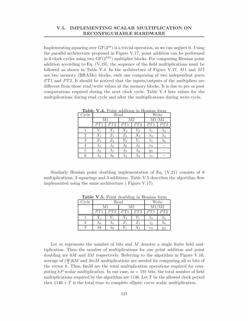
V.5. IMPLEMENTING SCALAR MULTIPLICATION ONRECONFIGURABLE HARDWARE
Implementing squaring over GF(2m) is a trivial operation, so we can neglect it. Usingthe parallel architecture proposed in Figure V.17, point addition can be performedin 6 clock cycles using two GF(2191) multiplier blocks. For computing Hessian pointaddition according to Eq. (V.19), the sequence of the field multiplications must befollowed as shown in Table V.4. In the architecture of Figure V.17, M1 and M2are two memory (BRAMs) blocks, each one comprising of two independent portsPT1 and PT2. It should be noticed that the inputs/outputs of the multipliers aredifferent from those read/write values at the memory blocks. It is due to pre or postcomputations required during the next clock cycle. Table V.4 lists values for themultiplications during read cycle and after the multiplications during write cycle.
Table V.4. Point addition in Hessian formCycle Read Write
M1 M2 M1/M2PT 1 PT 2 PT 1 PT 2 PT 1 PT 2
1 Y1 X1 X2 Y2 λ1 λ2
2 X1 Z1 Z2 X2 λ3 λ4
3 Z1 Z2 Y2 Y1 λ5 λ6
4 λ1 λ2 λ6 λ5 x3 −5 λ2 λ1 λ3 λ4 y3 −6 λ5 λ6 λ4 λ3 z3 −
Similarly Hessian point doubling implementation of Eq. (V.21) consists of 6multiplications, 3 squarings and 3 additions. Table V.5 describes the algorithm flowimplemented using the same architecture ( Figure V.17).
Table V.5. Point doubling in Hessian formCycle Read Write
M1 M2 M1/M2PT 1 PT 2 PT 1 PT 2 PT 1 PT 2
1 X1 Y1 X1 Y1 λ4 λ9
2 λ9 λ4 Z1 Z1 z2 λ8
3 λ8 λ9 Y1 X1 x2 y2
Let m represents the number of bits and M denotes a single finite field mul-tiplication. Then the number of multiplications for one point addition and pointdoubling are 6M and 3M respectively. Referring to the algorithm in Figure V.10,average of (m
2 )6M and 3mM multiplications are needed for computing all m bits ofthe vector k. Thus, 6mM are the total multiplication operations required for com-puting kP scalar multiplication. In our case, m = 191 bits, the total number of fieldmultiplications required by the algorithm are 1146. Let T be the allowed clock periodthen 1146 × T is the total time to complete elliptic curve scalar multiplication.
121

V. A Generic Coprocessor For Elliptic Curve Scalar Multiplication onHardware
V.5.2 Montgomery point multiplication
Referring to the algorithm of Figure V.14, each bit of vector k is tested from left toright (in descending order).
For each test bit (zero or one), both point addition (Madd) and point dou-bling (Mdouble) operations are performed. However, order of the arguments is re-versed: if the test bit is ‘1’, Mdouble(X2, Z2), Madd(X1, Z1,X2, Z2) are computedand Mdouble(X1, Z1), Madd(X2, Z2,X1, Z1) otherwise. The algorithms in FiguresV.13 and V.12 describe the sequence of the instructions for Madd and Mdoubleoperations respectively.
Tables V.6 and V.7 describe the multiplications performed for both point addi-tion and point doubling operations in three normal clock cycles when test bit is ’1’or ’0’ respectively. The notations used for the algorithms in Figures V.13 and V.12for point addition and point doubling were kept the same. M1 and M2 representtwo memory blocks (BRAMs) each one with two independent ports PT1 and PT2.Some required arithmetic operations (squaring etc.) need to be performed duringread/write cycles at the memories before and after the multiplication operations.
Table V.6. kP computation, if test-bit is ‘1’Cycle Read Write
M1 M2 M1/M2PT 1 PT 2 PT 1 PT 2 PT 1 PT 2
1 X1 Z2 Z1 X2 P Q2 X2 Z2 Z2 T1 Z2=Z3 X2=X3
3 P Q Q T2 X1=X ′ Z1=Z ′
The resultant vectors X1,Z1,X2,Z2, are updated at the memories after the com-pletion of point addition and doubling operations using 3 clock cycles for each bit.Total time for whole 191-bit test vector is therefore 191×3×T , T represents allowedfrequency.
Table V.7. kP computation, if test-bit is ‘0’Cycle Read Write
M1 M2 M1/M2PT 1 PT 2 PT 1 PT 2 PT 1 PT 2
1 X2 Z1 Z2 X1 P Q2 X1 Z1 Z1 T1 Z1=Z3 X1=X3
3 P Q Q T2 X2=X ′ Z2=Z ′
V.5.3 Implementation summary
All finite field arithmetic blocks and then the kP computational architecture wereimplemented on a VirtexE XCV3200e-8bg560 device by using Xilinx Foundation
122

V.5. IMPLEMENTING SCALAR MULTIPLICATION ONRECONFIGURABLE HARDWARE
Table V.8. Design Implementation SummaryDesign Device CLB Timings
(XCV) slicesInversion in GF (2191) 3200E 1312 1.9ηsBinary Karatsuba Multiplier 3200E 8721 43.1ηs1 Field Multiplication 100.1ηsPoint addition + Point 3200E 18300 300.3ηs (if bit = ‘0’)doubling in Hessian Form 900.9ηs (if bit = ‘1’)Point Multiplication 3200E 19626 & 114.71µsin Hessian form 24 BRAMsPoint addition + Point doubling 3200E 18300 300.3ηs(Montgomery Point Multiplication) (3 Multiplications)Point Multiplication 3200E 19626 & 59.26µs(Montgomery Point Multiplication) 24 BRAMs
Tool F4.1i for design entry, synthesis, testing, implementation and verification ofresults. Table V.8 lists timing performances and occupied resources by the saidarchitectures.
Elliptic curve point addition and point doubling do not participate directly asa single computational unit in this design; however parallel computations for bothpoint addition and point doubling are designed together as it was shown in Fig-ure V.10. Both point addition and point doubling occupy 18300 (56.39 %) CLBslices and it takes 100.1ηs (at a clock speed of 9.99 MHz) to complete one executioncycle. As it was mentioned in Section V.3.1, six and three cycles are needed forcomputing point addition and point doubling in Hessian form, respectively. Thusthe total consumed time for computing each iteration of the algorithm of FigureV.10 is 900.9η if the corresponding bit is one and 300.3ηs otherwise. Therefore,scalar point multiplication in Hessian form is the time to complete m/2 point ad-ditions (in average) and m point doublings. For our case m=191, the total time istherefore (191/2)(600.6) + 191(300.3) = 114.71µs. Point multiplication in Hessianform uses affine coordinates and therefore no time has been consumed in coordinatesconversion.
Similarly, two and one multiplications are needed to perform Montgomery pointmultiplication, thus consuming 100.1ηs and 200.2ηs for point doubling and pointaddition respectively. Each iteration of the algorithm thus consumes 300.3ηs for 3multiplications. For our case m = 191, total time is therefore 191(300.3) = 57µsfor elliptic curve scalar multiplication. Inversion is performed at the end. It takes19 clock cycles to perform one inversion in GF (2191) occupying 1312 CLB slices.The CLB slices for inversion in fact are the FPGA resources occupied for squaringoperations only and the multiplier blocks are the same used for point addition andpoint doubling. The total time is the sum of the time for the scalar multiplicationand the time to perform inversion for coordinate conversion i-e 57.36 + 1.9 = 59.26µs.
123

V. A Generic Coprocessor For Elliptic Curve Scalar Multiplication onHardware
The architecture for elliptic curve scalar multiplication in both cases (Hessianform & Montgomery point multiplication) occupies 19626 (60 %) CLB slices, 24(11%) BRAMs and performs at the rate of 100.1ηs (9.99 MHz). The design forKaratsuba Multiplier in GF(2191) occupies 8721 (26.87%) CLB slices and one fieldmultiplication is performed in 43.1ηs.
V.6 Performance comparison
Table V.9 provides a quick comparison of the existing FPGA’s implementationsof elliptic curve scalar multiplication over GF(2m). That table sums up the lastthree years state of the art implementations, where most of the works featured havebeen published this same year. A microcoded EC processor in [72] is implementedon Annapolis Microsystems Wildstar board. For this design, EC multiplication isexecuted in 4300µs, 8300µs, and 11100µs for GF(2113), GF(2155), and GF(2173)respectively. An efficient VLSI EC processor in [89] support EC scalar
multiplication both in GF(p) and GF(2n). Achieved results for a 160-bit ECscalar multiplication are 1210µs and 190µs for GF(p) and GF(2n) respectively. Ageneric VLSI architecture in [35] implements cryptographic primitives over variousfields. It consumes 6950µs to compute point multiplication using a repeated double-and-add algorithm. Another reconfigurable system on chip ECC implementation isreported on a special architecture AT94K40 from Atmel that integrates various com-ponents including an AVR 8-bit RISC micro-controller, several peripheral devicesand up to 36K bytes SRAM within a single chip. That design execute EC operationin just 1400µs. All other designs [66, 92, 91, 16] implements EC scalar multiplicationon single chip FPGA.
Table V.9 also includes a speedup factor that measures how much our design isfaster than the others. It is obtained by dividing kP computational time of a givendesign over the time taken by our design. As it can be seen, our design shows animprovement ranging from 2.55 times up to 316 times of speedup.
The design presented in [89] can handle arbitrary fields and elliptic curves with-out changing its hardware configuration, while those parameters have been fixed inour implementation. However the design in [89] was implemented on a traditionalASIC chip, where the flexibility for design changes is quite limited or many timeseven inexistent. In our approach on the other hand, taking advantage of the reconfig-urability feature of the platform selected, we preferred to optimize the performanceof our design for a given field while the possibility to reconfigure the design for otherparameters can still be instrumented.
Table V.9 provides a list of reported designs for elliptic curve scalar multipli-cation over GF(2m) implemented on FPGAs or VLSI. From that list, our designsobtained the fastest computation time needing only 114.71µs in Hessian form and59.26µs using Montgomery point multiplication algorithm.
124

V.7. CONCLUSIONS
Table V.9. GF(2m) Elliptic Curve Point Multiplication Hardware PerformanceComparisonEC scalar Field Platform Freq. kP Speed Multiplier Blockmultiplication MHz (µs) up Utilized
[72] GF(2113) Annapolis 4300 76 Serial multiplierGF(2155) Micro Sys. 8300 148GF(2173) Wildstar board 11100 198
[89] GF(2160) 0.13µ CMOS 510.2 190 3.39 64-bit multiplierASIC
[35] GF(2176) 0.25µ CMOS 50 6950 124 1024-bit adder
[66] GF(2167) XCV400E 76.7 210 3.75 16-bit multiplier167-bit squarer
[91] GF(2191) XCV4000XL 11820 211 Not17710 316 specified
[38] GF(2163) XCV2000E 143 2.55 64-bit shift and addGF(2193) 187 3.34 multiplier
[31] GF(2113) AT94K40 12 1400 25 24-bit Karatsuba
[16] GF(2191) XCV1000BG 50 270 4.82 4 2-Bit level LFSR36 2270 40 1 Massey-Omura
Hessian GF(2191) XCV3200E 9.99 114.71 Two GF(2191) BinaryForm karatsuba multiplier
Montgomery GF(2191) XCV3200E 9.99 59.26 Two GF(2191) BinaryPoint Mult. karatsuba multiplier
V.7 Conclusions
In this chapter, a generic architecture for elliptic curve point multiplication waspresented. The proposed architecture is based on parallel implementations of eachstage of the kP computation process. Although the architecture was optimized forreconfigurable devices, it can be applied to other hardware platforms (such as VLSI)with minor modifications.
The structure presented in this chapter constitutes a generic architecture for thescalar multiplication in Hessian form as well as for Montgomery point multiplicationdefined over GF(2191). The resulting performance time for the scalar point multi-plication operation in Hessian form is of 114.71µs, while it takes just 59.26µs tocomplete Montgomery point multiplication. Therefore the Weierstrass form utiliz-ing the Montgomery group formulation can be computed in about half the executiontime consumed by the time needed in the case of the Hessian form.
Two major factors contribute in achieving high performances for our architec-ture. First, parallel strategies that were applied throughout the design ranging fromfinite field arithmetic to scalar point multiplication. The efficient field units (multi-pliers, squarers, etc) were designed and optimized for shortest possible data criticalpaths. Second, we investigated for the best use of those basic building blocks thatincludes the structural arrangements related to the computation of point additionand point doubling as described in Table V.3. As a whole, implementation of elliptic
125

V. A Generic Coprocessor For Elliptic Curve Scalar Multiplication onHardware
curve scalar multiplications on FPGA devices yields efficient architectures, showinga good balance between speed and time.
Future work includes the search for faster algorithms for elliptic curve scalar mul-tiplication, the implementation of other design strategies and comparison betweenthem.
126

Chapter VI
Conclusions
The main focus of this thesis was the study and analysis of cryptographic algo-rithms (CA) for their compact and high-speed implementations on reconfigurablelogic platform by using optimized techniques with respect to both time and area.Three main goals were formulated to make a comprehensive study of cryptographicalgorithms: (1) a study of general symmetric block-cipher cryptographic algorithmsto develop general guidelines for implementing them in FPGAs which were appliedto Data Encryption Standard (DES), (2) a study of architectural alternatives forimplementing a modern and standard symmetric block-cipher (AES) in FPGAs,and (3) a study of basic operations required by public-key cryptography based onelliptic curves (ECC).
To achieve our first goal, we searched for the most common and fundamentaloperations in symmetric block ciphers. It was observed that most block cipherswere generally constructed using bit-wise logic, permutation and substitution op-erations. Another important feature was their iterative nature where a single en-cryption was concluded by repeating n iterations of the algorithm. We presentedsome novel techniques for implementing such operations on reconfigurable devices.We also explained whole design procedure for an FPGA architecture. Some designrecommendations were provided for the optimization of an FPGA design leading tohigh performance circuits. A case of study about DES is presented. Therefore, ourcontributions obtained from this goal are: we develop general guidelines for the re-configurable implementation of block ciphers, and we present a compact and efficientimplementation of DES. Those contributions were reported in [85, 27].
To achieve our second goal, We deeply revised all steps in AES algorithm. Variousoptions for its implementations were discussed considering performance, cost andarea limitations on reconfigurable platform. Consequently, several AES designs forencryptor, encryptor/decryptor, and decryptor cores using iterative and pipelineddesign strategies were developed which were reported in [83, 82, 84, 75, 80].
127

CHAPTER VI. CONCLUSIONS
In the first part of this study, an encryptor core was developed. Iterative andpipelined architectures were devised for it resulting a pipeline architecture requiringmore area but achieving n times better throughput as compared to the iterativedesign.
For a full encryptor/decryptor core, we found that one of the most costly trans-formations in terms of area are byte substitution (BS) and its corresponding inverse(IBS) for AES. They are typically implemented as a substitution box (S-Box). Bothtransformations require a multiplicative inverse (MI) step plus an affine transforma-tion (AF). Applying AF before MI produces S-Box for encryption. For decryption,inverse of AF (IAF) is applied after MI.
Since cost of BS and IBS is mainly due to MI step, in fully pipelined encryp-tor/decryptor core, we devised a technique for sharing a single MI module for bothprocesses. Two implementations for MI were considered: by using pre-computedvalues stored in look-up tables (built-in memory modules) or by calculating valueson-the-fly using composite field. AES encryptor/decryptor core using look-up tablemethod for AES S-Box was faster but with high memory requirements. On the otherhand, the composite field strategy yielded a less efficient but memory free architec-ture which can be suitable for cheap and portable FPGAs. In any case, our designsreported in [84] are competitive, or in some cases, even better compared to previousresults.
Another consideration in developing a fully pipelined encryptor/decryptor corewas made on MixColumn and Inverse MixColumn transformation (MC and IMC).A separated implementation for MC and IMC steps is a straightforward approach.However, we observed that IMC can be implemented by applying a small modifi-cation followed by MC. We evaluated both approaches whose results were reportedin [75, 80]. We observed that FPGA resources were saved and the critical path fordecryption was reduced resulting high throughput for the AES encryptor/decryptorcore with a modified MC transformation.
Regarding AES, our last architectural consideration was focused on designinga decryptor core only. It was firstly motivated to show the difference between en-cryption and decryption timing for AES. In fact, due to asymmetric nature of AES,different steps are used for encryption/decryption and steps involved in decryptionprocess are more intensive resulting higher timing for decryption. AES decryptorcore was realized by isolating the data-path for decryption from the most efficientencryptor/decryptor core. Further, some steps were combined exploiting the CLBfour-input/one-output configuration. S-Box/inverse S-Box were implemented usinglook-up table method. Inverse MixColumn was performed using MixColumn plus asmall modification. Using this strategy, decryption timing was very close to that ofencryption.
For all seven AES architectures, key schedule implementations were also madeand all AES architectures were optimized with respect to both area and time. Asa result, high speed and economical (occupying less hardware resources) AES ar-chitectures were achieved. In summary, our results for AES FPGA implementations
128

were either competitive or better than previous state-of-the-art AES FPGA imple-mentations reported in the literature to-date.
The third goal of this dissertation was dedicated to public-key cryptosystembased on Elliptic Curve Cryptography (ECC). Achieved results for this work werereported in [76, 87, 81, 86, 88]. We developed FPGA implementations for performingthe most important operation in ECC: elliptic curve scalar multiplication (or pointmultiplication). We adopted a three-stage model in which basic blocks from thelower stages were used to implement operations required in higher stages.
In the first stage, we considered the implementation of finite field Arithmetic: ad-dition/subtraction, squaring, multiplication, and inversion in GF(2m). Implementingaddition/subtraction, squaring and then reduction for all of them is trivial. How-ever, multiplication in GF(2m) is complicated. We introduced binary Karatsubamultiplier, a variant of Karatsuba-Ofman multiplier which is a useful approach withrespect to both time and area. Inversion in GF(2m) is a sequence of multiplicationand squaring operations. The common feature for implementing finite field arith-metic operations was to exploit maximum parallelism and to reduce critical pathsproducing less execution time.
Second stage for performing elliptic curve scalar multiplication is elliptic curvearithmetic: point addition and doubling. Both operations need building blocks formultiplication and squaring from first stage. Since, multiplication in GF(2m) oc-cupies large space, a study was made for maximum multipliers allowed by targetFPGA that can produce maximum throughput at this stage. It was found that weare limited to two multipliers in parallel on VirtexE device XCV3200.
In the third stage of our model, the elliptic curve scalar multiplication was finallyimplemented by using building blocks from the two previous stages. A generic archi-tecture was proposed for the implementation of elliptic curve scalar multiplication.That architecture was further used for FPGA implementations of Hessian form ofElliptic curve and Montgomery point multiplication. Due to careful considerationsat all stages of the design, our results improve existing FPGA implementations ofElliptic curve scalar multiplication reported in the literature to-date.
Concluding Remarks
In this thesis work, we have analyzed cryptographic algorithms for high-speed im-plementation on reconfigurable logic platform. Concluding remarks for this work aredrawn as follows:
1. We focus on both symmetric and asymmetric cryptographic algorithms. Thestudy about symmetric algorithms is mainly dedicated to block ciphers. Ba-sic structure, design principles and most frequent operations in block ciphersare explained. It has been observed that modern block ciphers are more ef-ficient and resistive but they exhibit similar structure: same operations suchas transposition and substitution (in improved form), which are repeated for
129

CHAPTER VI. CONCLUSIONS
number of times. Asymmetric algorithms involve complex mathematical oper-ations however some useful efforts have been observed for making them simpleand proficient.
2. The concept of parallelism can be effectively used for symmetric block ciphers.Parallel operations in a block cipher can easily be detected. Basic buildingblocks in a block cipher can be opted for several combinations in a parallelway. In asymmetric ciphers, parallel operations are not common. However, aneffort has been in this thesis work for developing parallel algorithms for them.
3. Reconfigurable logic platform proves to be a suitable platform for implement-ing cryptographic algorithms. Basic structure of reconfigurable hardware de-vices is found to be suitable for implementing basic primitives in cryptographicalgorithms. Moreover, high density FPGAs can accommodate big circuits dueto parallel approaches for cryptographic algorithms. Reconfigurable logic plat-form offers several useful benefits for cryptographic algorithm implementationsbut it may not be a right choice for all kinds of security applications or allkinds of cryptographic algorithms.
4. Parallelism is a key feature of this thesis work for achieving high design perfor-mances equally useful for other similar applications. It requires a deep analysisat algorithm level in searching parallel operations among cryptographic algo-rithms. It works at design level in designing involved operations accordingto the structure of target devices. It is useful when hardware resources allowmultiple building blocks for a single operation. However, the concept of par-allelism is not based on occupying unlimited hardware resources for achievinghigh performances but on the quality work exploiting parallelism where it hasa worth.
5. Optimization is an essential task for an FPGA architecture in improving de-sign performance with respect to time and space. It requires manual work ineliminating overheads in a design: using schematic components for an FPGAdesign is cumbersome as compared to HDLs but it facilitates a synthesis toolwhile placing and routing design components. Similarly, Synthesis tools allowa designer to put several time and area constraints according to design specifi-cations. However, synthesis tools takes long time (in hours) in achieving thesegoals and sometimes also fail.
Future Work
We believe that on the basis of this dissertation work, there are strong chances formore contributions in the field of cryptography. As a future work, a short descriptionof some of them is provided below:
1. A hardware-software approach for implementing cryptographic algorithms canbe helpful in achieving high performances. Some parts in a cryptographic
130

algorithm can efficiently be implemented in software and some of them inhardware. Modern FPGAs include microcontrollers besides their standardresources and also establish an interface for communication between them.Such type of FPGAs can help in reducing communication overheads betweensoftware-hardware methods.
2. Faster algorithms for the basic transformations of cryptographic algorithmsare always investigated for improving overall performances of cryptographicschemes. New techniques need to be explored. As an example, ECC implemen-tations in this thesis are based on addition-doubling method for EC arithmetic.A new technique based on addition-halving [40] for EC could be an option forimproving design performance.
3. Similar cryptographic schemes can be implemented for comparison betweentiming and occupied hardware resources by them. ECC is considered for pro-viding same security at shorter key length as compared to cotemporary algo-rithms such as RSA. A comparison between ECC and RSA implementationswould be interesting. Similarly, Koblitz curves for ECC are believed to be moresecure. A comparison of Koblitz curve implementations with other curves canprovide cost estimations for achieving higher security.
4. Cryptographic solutions for smart cards pose a challenge since security is de-sired under limited hardware resources. Compact and fast cryptographic solu-tions for smart cards can be a useful and challenging task.
5. Hardware implementations provide physical security. But it is still an openquestion whether they are secure against other possible attacks such as sidechannel attacks.
6. In this thesis work, reconfigurable logic platform was chosen for implementingcryptographic algorithms. However, other possible options (software methodsusing embedded processors, VLSI) need to be explored for resolving time andspace issues.
7. Several design strategies can be adopted achieving high data rates for cryp-tographic algorithms. A comparison for iterative and pipeline approaches wasincluded in this thesis work. Use of other design strategies such as inner-roundor outer-round looping could be an effort to determine cost for the design interms of hardware area for high speed.
8. In recent years, security applications using cryptographic algorithms have beenincreased. To combat current security threats, it is required to provide securitysolutions for large number of security applications within their own framework.This thesis work is required to be extended to other cryptographic algorithmssuch as streams ciphers.
131


Bibliography
[1] Polycom. URL: http://www.polycom.com/common/pw item show doc/0,1276,3076,00.pdf.
[2] Nokia 6225 Phone. URL: http://www.nokiausa.com/phones/6225.
[3] Ericcson. URL: http://www.erricson.com/.
[4] International Telecommunication Union. URL: http://www.itu.int/home/index.html.
[5] European Telecommunications Standards Institute. URL: http://www.etsi.org/.
[6] IEEE 802 LAN/MAN Standards Committee. URL: http://grouper.ieee.org/groups/802/index.html.
[7] ETSI Technical Specification. Access transmission systems on metallic accesscables; Very High Speed Digital Subscriber Line (VDSL); Part 1: Functionalrequirements.
[8] Xilinx Virtex TM-E 1.8V Field Programmable Gate Arrays. URL:http://www.xilinx.com/xlnx/xweb/xil publications index.jsp.
[9] Xilinx Virtex TM-E 1.8V Field Programmable Gate Arrays. URL:www.xilinx.com.
[10] Hardware IP Cores of Advanced Encryption Standard AES-Rijndael. URL:http://ece.gmu.edu/crypto/rijndael.htm.
[11] High Performance Solution in Silicon: AES (Rijndael) Cores. URL:http://www.heliontech.com/core2.htm.
[12] ANSI T1E1.4, Sep. 1 1999. Draft Technical Document, Revision16, Very HighSpeed Digital Subscriber Lines; System requirements.
[13] Free-DES Core(2000), March 2000. URL: http://www.free-ip.com/DES/.
133

BIBLIOGRAPHY
[14] ANSI X9.63. Public Key Cryptography for the Financial Services Industry:Elliptic Curve Key Agreement and Key Transport Protocols, working draft.,August 1999.
[15] E. Bach and J. Shallit. Algorithmic number theory, Volume I: efficient algo-rithms. Kluwer Academic Publishers, Boston, MA, 1996.
[16] M. Bednara, M. Daldrup, J. Shokrollahi, J. Teich, and J. von zur Gathen. Re-configurable Implementation of Elliptic Curve Crypto Algorithms. In Proc. ofThe 9th Reconfigurable Architectures Workshop (RAW-02), Fort Lauderdale,Florida, U.S.A., April 2002.
[17] Guido Bertoni, Luca Breveglieri, Pasqualina Fragneto, Marco Macchetti, andStefano Marchesin. Efficient Software Implementation of AES on 32-bits plat-forms. In Proceedings of the CHESS 2002, pages 159–171, LNCS 2523, 2002.
[18] E. Biham. A fast new DES implementation in software. In 4th Int. Workshopon Fast Software Encryption, FSE97, pages 260–271, Haifa, Israel, January1997. Springer-Verlag, 1997.
[19] Matt Bishop. An application of a fast Data Encryption Standard implemen-tation. In Computing Systems, 1(3), pages 221–254, Summer 1988.
[20] certicomTM. ECC Tutorial. http://www.certicom.com/index.php?action=ecc tutorial,home.
[21] Stephen Charlwood and Philip James-Roxby. Evaluation of the XC6200-Series Architecture for Cryptographic Application. In FPL 98, Lecture Notesin Computer Science 1482, pages 218–227. Springer-Verlag Berlin Heidelberg2003, August/September 1998.
[22] L. Childs. A concrete introduction to higher algebra. Springer-Verlag BerlinHeidelberg, Germany, 1995.
[23] D. V. Chudnovsky and G. V. Chudnovsky. Sequences of numbers generated byaddition in formal groups and new primality and factorization tests. Advancesin Applied Math., 7:385–434, 1986.
[24] Joan Daemen and Vincent Rijmen. The design of Rijndael, AES-The AdvanceEncryption Standard. Springer-Verlag Berlin Heidelberg, New York, 2002.
[25] A. Dandalis, V.K. Prasanna, and J.D.P Rolim. A Comparitive Study of Per-formance of AES Candidates using FPGAs. In The Third AES3 CandidateConference, New York, April 2000.
[26] Marc Davio, Yvo Desmedt, Jo Goubert, Frank Hoornaert, and Jean JacquesQuisquater. Efficient hardware and software implementations for the DES. InProc. of Crypto’ 83, pages 144–146, August 1984.
134

BIBLIOGRAPHY
[27] Arturo Dıaz-Perez, Nazar A. Saqib, and Francisco Rodrıguez-Henriquez.Some Guidelines for Implementing Symmetric-Key Cryptosystems onReconfigurable-Hardware. In (Accepted for) IV Jornadas de ComputacionReconfigurable y Aplicaciones, Barcelona, Spain, September.
[28] H. Eberle. A high speed DES implementation for network applications. In Ad-vances in Cryptology-CRYPTO‘92, Lecture Notes in Computer Science, pages521–539, Berlin, Germany, September 1992. Springer-Verlag, 1992.
[29] H. Eberle and C.P. Thacker. A 1 Gbit/second GaAs DES chip. In Proc. IEEE1992 Custom Integrated Circuits Conference, pages 19.7/1–4, New York,USA,1992. Springer-Verlag, 1992.
[30] J. Elbirt, W. Yip, B. Chetwyned, and C. Paar. A FPGA Implementationand Performance Evaluation of the AES Block Cipher Candidate AlgorithmFinalist. In The Third AES3 Candidate Conference, New York, April 2000.
[31] M. Ernst, M. Jung, and F. Madlener et. al. A Reconfigurable System on ChipImplementation for Elliptic Curve Cryptography over GF (2n). CryptographicHardware and Embedded Systems - CHES 2002, 4th International Workshop,Redwood Shores, CA, USA, August 13-15, 2002, Revised Papers, 2523:381–399, August 2003.
[32] David C. Feldmeier. A high speed crypt program, April 1989. Technical MemoTM-ARH-013711.
[33] Kris Gaj and Pawel Chodowiec. Comparison of the Hardware Performanceof the AES Candidates using Reconfigurable Hardware. In The Third AES3Candidate Conference, New York, April 2000.
[34] Brian Gladman. The AES Algorithm (Rijndael) in C and C++. URL:http://fp.gladman.plus.com/cryptography technology/rijndael/.
[35] J. Goodman and A.P. Chandrakasan. An Energy-Efficient ReconfigurabilityPublic-Key Cryptography Processor. IEEE Journal of Solid-State Circuits,36(11):1808–1820, November 2001.
[36] J. Guajardo and C. Paar. Efficient Algorithms for Elliptic Curve Cryptosys-tems. In Advances in Cryptology-CRYPTO 97, LNCS 1294, pages 342–356,Springer-Verlag, Berlin, Germany, 1997.
[37] J. Guajardo and C. Paar. Efficient Algorithms for Elliptic Curve Cryptosys-tems. In B. S. Kaliski Jr. (editor) Advances in Cryptology —CRYPTO 97Lecture Notes in Computer Science, 1294:342–356, 1997.
[38] N. Gura, S. Shantz, and H. Eberle et. al. An End-to-End Systems Approach toElliptic Curve Cryptography. Cryptographic Hardware and Embedded Systems
135

BIBLIOGRAPHY
- CHES 2002, 4th International Workshop, Redwood Shores, CA, USA, August13-15, 2002, Revised Papers, 2523:349–365, August 2003.
[39] D. Hankerson, J. Lopez-Hernandez, and A. Menezes. Software Implementa-tion of Elliptic Curve Cryptography Over Binary Fields. Cryptographic Hard-ware and Embedded Systems - CHES 2000, Second International Workshop,Worcester, MA, USA, August 17-18, 2000, Proceedings, 1965:1–24, August2000.
[40] Darrel Hankerson, Alfred Menezes, and Scott Vanstone. Guide to EllipticCryptography. Springer-Verlag Newyork, Inc., 2004.
[41] M. A. Hasan, M. Z. Wang, and V. K. Bhargava. A modified Massey-Omuraparallel multiplier for a class of finite fields. IEEE Transactions on Computers,42(10):1278–1280, November 1993.
[42] T. Ichikawa, T. Kasuya, and M. Matsui. Hardware Evaluation of the AesFinalists. In The Third AES3 Candidate Conference, New York, 2000.
[43] ISO/IEC 15946. Information technology - Security Techniques - Cryptographictechniques based on Elliptic Curve. Committee Draft (CD),, 1999. URL:http://www.iso.ch/iso/en/CatalogueDetailPage.CatalogueDetail?CSNUMBER=31077.
[44] T. Itoh and S. Tsujii. A Fast Algorithm for Computing Multiplicative Inversesin GF(2m) using normal basis. Information and Computing, 78:171–177, 1988.
[45] J.P. Kaps and C. Paar. Fast DES implementations for FPGAs and its ap-plication to a Universal key-search machine. In Proc. 5th Annual Workshopon selected areas in cryptography-Sac’ 98, pages 234–247, Ontario, Canada,August 1998. Springer-Verlag, 1998.
[46] Philip R. Karn. Karns DES implementation source code.
[47] N. Koblitz. Introduction to elliptic curves and modular forms. Springer-VerlagBerlin Heidelberg, Germany, 1984.
[48] N. Koblitz. CM-curve with good cryptographic properties. In Advances inCryptology, Crypto’91, pages 279–287. Springer-Verlag, 1992.
[49] J. Leonard and W.H. Magione-Smith. A case study of partially evaluated hard-ware circuits: key specific DES. In Proc. Field-Programmable Logic and Ap-plications, FPL’ 97, pages 234–247, London, UK, September 1997. Springer-Verlag, 1997.
[50] J. Lopez and R. Dahab. Fast multiplication on elliptic curves over GF (2m)without precomputation. Cryptographic Hardware and Embedded Systems,First International Workshop, CHES’99, Worcester, MA, USA, August 12-13, 1999, Proceedings, 1717:316–327, August 1999.
136

BIBLIOGRAPHY
[51] A.K. Lutz, J. Treichler, F.K. Gurkaynak, H. Kaeslin, G. Basler, A. Erni, S. Re-ichmuth, P. Rommens, S. Oetiker, and W. Fitchtner. 2 Gbits/s HardwareRealization of RIJNDAEL and SERPENT-A Comparative Analysis. In Pro-ceedings of the CHESS 2002, pages 171–184, LNCS 2523, 2002.
[52] J.V. McCanny Maire McLoone. High Performance FPGA Rijndael AlgorithmImplementation. In Proceedings of the CHESS 2001, pages 68–80, LNCS 2162,2001.
[53] R. J. McEliece. Finite Fields for Computer Scientists and Engineers. KluwerAcademic Publishers, Boston, MA, 1987.
[54] R. J. McEliece. Finite Fields for Computer Scientists and Engineers. KluwerAcademic Publishers, Boston, MA, 1987.
[55] M. McLoone and J.V. McCanny. High-performance FPGA implementationof DES using a novel method for implementing the key schedule. IEE Proc.:Circuits, Devices & Systems, 150(5):373–378, October 2003.
[56] A. Menezes, P. Van Oorschot, and S. Vanstone. Handbook of Applied Cryp-tography. CRC Press, Boca Raton, FL, 1997.
[57] A. J. Menezes, I. F. Blake, X. Gao, R. C. Mullen, S. A. Vanstone, andT. Yaghoobian. Applications of Finite Fields. Kluwer Academic Publishers,Boston, MA, 1993.
[58] A. J. Menezes, Paul C. van Oorschot, and Scott A.Vanstone. Handbook ofApplied Cryptography. CRC Press, Boca Raton, Florida, 1996.
[59] A.J. Menezes. Elliptic Curve Public Key Cryptosystems. Kluwer AcademicPublishers, 1993.
[60] V. Miller. Uses of elliptic curves in cryptography. In H. C. Williams (edi-tor) Advances in Cryptology — CRYPTO 85 Proceedings Lecture Notes inComputer Science, 218:417–426, January 1985.
[61] M. Morii, M. Kasahara, and D. L. Whiting. Efficient bit-serial multiplicationand the discrete-time Wiener-Hopf equation over finite fields. IEEE Transac-tions on Information Theory, 35(6):1177–1183, 1989.
[62] S. Morioka and A. Satoh. An Optimized S-Box Circuit Architecture for LowPower AES Design. In Proceesings of the CHESS 2002, pages 172–183, LNCS2523, 2002.
[63] Motorola. URL: http://www.motorola.com/LMPS/RNSG/federal/products/secure telecom/CipherTAC 2000.html.
[64] Randall K. Nichols and Panos C. Lekkas. Wireless Security: Models, Threats,and Solutions. McGraw Hill, 2000.
137

BIBLIOGRAPHY
[65] NIST. Announcing the ADVANCED ENCRYPTION STANDARD(AES). Federal Information Standards Publication, Nov. 2001. URL:http://csrc.nist.gov/CryptoToolkit/aes/index.html.
[66] G. Orlando and C. Paar. A High-Performance Reconfigurable Elliptic CurveProcessor for GF (2m). Cryptographic Hardware and Embedded Systems -CHES 2000, Second International Workshop, Worcester, MA, USA, August17-18, 2000, Proceedings, 1965:41–56, August 2000.
[67] G. Orlando and C. Paar. A Scalable GF (p) Elliptic Curve Processor Archi-tecture for Programmable Hardware. Cryptographic Hardware and EmbeddedSystems - CHES 2001, Third International Workshop, Paris, France, May14-16, 2001, Proceedings, 2162:348–363, May 2001.
[68] IEEE P1363. Standard specifications for public-key cryptography. IEEE stan-dards documents, ”http://grouper.ieee.org/groups/1363/”, draft version 7 edi-tion, September 1998.
[69] C. Paar. Efficient VLSI Architectures for Bit Parallel Computation in GaloisFields: PhD thesis: Universitat GH Essen,1994. VDI Verlag.
[70] C. Paar. A new architecture for a parallel finite field multiplier with lowcomplexity based on composite fields. IEEE Transactions on Computers,45(7):856–861, July 1996.
[71] C. Patterson. High performance DES encryption in Virtex FPGAs using Jbits.In Field-programmable custom computing machines, FCCM’ 00, pages 113–121, Napa Valley, CA, USA, January 2000. IEEE Comput. Soc., CA, USA,2000.
[72] philip:des. Philip R. Karn. Technical Memo TM-ARH-013711.
[73] ANSI X9.17 (Revised):. National Standards for financial institution key man-agement (wholesale), American Bankers Association, 1986.
[74] F. Rodrıguez-Henrıquez and C. K. Koc. On fully parallel Karatsuba Mul-tipliers for GF (2m). In International Conference on Computer Science andTechnology (CST 2003), Cancun, Mexico, May 2003.
[75] F. Rodrıguez-Henriquez, N. A. Saqib, and A. Dıaz-Perez. 4.2 Gbit/s Single-Chip FPGA Implementation of AES Algorithm. In ELECTRONICS LET-TERS, volume 39, pages 1115–1116. Springer-Verlag Berlin Heidelberg 2003,July 2003.
[76] F. Rodrıguez-Henriquez, N. A. Saqib, and A. Dıaz-Perez. A Fast ParallelImplementation of Elliptic Curve Point Multiplication over GF(2m). Micro-processor and Microsystems, 28:329–339, August 2004.
138

BIBLIOGRAPHY
[77] Francisco Rodrıguez-Henriquez. New Algorithms and Architectures for Arith-metic in GF(2m) suitable for Elliptic Curve Cryptography, PhD thesis: OregonState University, 2000.
[78] K. Rosen. Elementary Number Theory and its Applications. Addison-Wesley,Reading, MA, 1992.
[79] Atri Rudra, Pardeep K. Dubey, Charanjit S. julta, Vijay Kumar, JodyulsR.Rao, and Pankaj Rohatgi. Efficient Rijndael Encryption Implementationwith Composite Field Arithmetic. In Proceedings of the CHESS 2001, pages171–184, LNCS 2162, 2001.
[80] N. A. Saqib, A. Dıaz-Perez, and F. Rodrıguez-Henriquez. Highly Opti-mized Single-Chip FPGA Implementations of AES Encryption and DecryptionCores. In X Workshop Iberchip, pages 117–118, Cartagena-Colombia, March2004.
[81] Nazar A. Saqib, Francisco Rodrıguez-Henriquez, and Arturo Dıaz-Perez. AParallel Architecture for Fast Computation of Elliptic Curve Scalar Multi-plication over GF(2m). In Proceedings of 18th International Parallel & Dis-tributed Processing Symposium (RAW 2004), page 144, Santa Fe, New Mexico,April. IEEE Computer Society Press.
[82] Nazar A. Saqib, Francisco Rodrıguez-Henriquez, and Arturo Dıaz-Perez. AESAlgorithm Implementation-An efficient Approach for Sequential and PipelineArchitecures. In Fourth Mexican International Conference on Computer Sci-ence, pages 126–130, Tlaxcala-Mexico, September 2003. IEEE Computer So-ciety Press.
[83] Nazar A. Saqib, Francisco Rodrıguez-Henriquez, and Arturo Dıaz-Perez. Se-quential and Pipelined Architecures for AES Implementation. In Proceedingsof the IASTED International Conference on Computer Science and Technol-ogy, pages 159–163, Cancun, Mexico, May 2003. IASTED/ACTA Press.
[84] Nazar A. Saqib, Francisco Rodrıguez-Henriquez, and Arturo Dıaz-Perez.Two Approaches for a Single-chip FPGA Implementation of an Encryp-tor/Decryptor AES Core. In FPL 2003, Lecture Notes in Computer Science2778, pages 303–312. Springer-Verlag Berlin Heidelberg 2003, 2003.
[85] Nazar A. Saqib, Francisco Rodrıguez-Henriquez, and Arturo Dıaz-Perez. ACompact and Efficient FPGA Implementation of the DES Algorithm. In(Accepted for) International Conference on Reconfigurable Computing andFPGAs (ReConFig04), Colima, Mexico, September 2004. Mexican Society forComputer Sciences.
[86] Nazar A. Saqib, Francisco Rodrıguez-Henriquez, and Arturo Dıaz-Perez. AGeneric Coprocessor For Elliptic Curve Scalar Multiplication on Hardware.Nova Science Publishers, New York, 2004. In press.
139

BIBLIOGRAPHY
[87] Nazar A. Saqib, Francisco Rodrıguez-Henriquez, and Arturo Dıaz-Perez. AParallel Architecture for Computing Scalar Multiplication on Hessian EllipticCurves. In International Symposium on Information Technology (ITCC 2004),pages 546–552, Las Vegas (NV), USA, April 2004. IEEE Computer SocietyPress.
[88] Nazar A. Saqib, Francisco Rodrıguez-Henriquez, and Arturo Dıaz-Perez. A Re-configurable Processor for High Speed Point Multiplication in Elliptic Curves.International Journal of Embedded Systems, ( In press for 2004 ), 2004.
[89] A. Satoh and K. Takano. A Scalable Dual-Field Elliptic Curve CryptographicProcessor. IEEE Transactions on Computers, 52(4):449–460, April 2003.
[90] B. Schneier. Applied Cryptography: Protocols, Algorithms, and Source Codein C. John Wiley & Sons, New York, 1996.
[91] N. Smart. The Hessian Form of an Elliptic Curve. Cryptographic Hardwareand Embedded Systems - CHES 2001, Third International Workshop, Paris,France, May 14-16, 2001, Proceedings, 2162:118–125, May 2001.
[92] N. Smart and E. Westwood. Point multiplication on ordinary elliptic curvesover fields of characteristic three. Applicable Algebra in Engineering, Commu-nication and Computing, 13:485–497, 2003.
[93] Sony. URL: http://www.sony.com/.
[94] William Stallings. CRYPTOGRAPHY AND NETWROK SECURITY: Pprin-ciples and Practice. Prentice Hall, Upper Saddle River, New Jersey 07458,1999.
[95] B. Sunar and C. K. Koc. Mastrovito multiplier for all trinomials. IEEETransactions on Computers, 48(5):522–527, May 1999.
[96] TCC. URL: http://www.tccsecure.com/csd4100.htm.
[97] W. Trappe and L.C. Washington. Introduction to Cryptography with CodingTheory. Prentice Hall, Inc., Upper Saddle River, NJ 07458, 2002.
[98] Joachim von zur Gathen and Michael Nocker. Computing special powersin finite fields: extended abstract. In Proceedings of the 1999 internationalsymposium on Symbolic and algebraic computation, pages 83–90. ACM Press,1999.
[99] B. Weeks, M. Bean, T. rozylowicz, and C. Ficke. Hardware Performance ofRound 2 Advanced Encryption Standard algorithms. In The Third AES3Candidate Conference, New York, April 2000.
[100] S. Wicker. Error control systems for digital communication and storage.Prentice-Hall, Englewood Cliffs, NJ, 1995.
140

BIBLIOGRAPHY
[101] S. B. Wicker and V. K. Bhargava (editors). Reed-Solomon Codes and TheirApplications. Prentice-Hall, Englewood Cliffs, NJ, 1994.
[102] D.C. Wilcox, L.G. Pierson, P.J. Robertson, E. L. Witzke, and K. Gass. ADES ASIC suitable for network encryption at 10 gbs and beyond. In CHESS99, pages 37–48, LNCS 1717, August 1999.
[103] K. Wong, M. Wark, and E. Dawson. A Single-chip FPGA Implementation ofthe Data Encryption Standard (DES) Algorithm. In IEEE Globecom Com-munication Conf., pages 827–832, Sydney, Australia, Nov. 1998.
[104] H. Wu and M. A. Hasan. Low complexity bit-parallel multipliers for a class offinite fields. IEEE Transactions on Computers, 47(8):883–887, August 1998.
[105] ANSI X9.62. Federal Information Processing Standard (FIPS) 46, NationalBureau Standards, January 1977.
141


GLOSSARY
Area (hardware) Hardware resources occupied by the design. In terms of FPGAs,hardware area includes number of CLBs, memory blocks, IOBs, etc.
Block cipher A type of symmetric key cipher which operates on groups of bits ofa fixed length, termed blocks.
BlockRAMs Built-in memory modules in FPGAs.
Brute force attack A brute force attack is brute force search for key space: tryingall possible keys to recover plaintext from ciphertext.
Cipher A cipher is an algorithm for performing encryption and decryption.
Ciphertext An encrypted message is called ciphertext.
CLB Configurable logic block (CLB) is a programmable unit in FPGAs. A CLBcan be reconfigured by the designer resulting a functionally new digital circuit.
Confusion Confusion makes the output dependent on the key. Ideally every keybit influences every output bit.
Decryption The process of retrieving plaintext from ciphertext is called decryp-tion.
Plaintext Diffusion makes the output dependent on the previous input (plain-text/ciphertext). Ideally each output bit is influenced by every input bit.
Downstream It defines the transmission from line terminal to network terminal(from customer to network premise).
Elliptic curve In mathematics, elliptic curves are defined by certain cubic (thirddegree) equations. They find applications in cryptography.
Elliptic curve cryptography Elliptic curve cryptography (ECC) is an approachto public-key cryptography based on the mathematics of elliptic curves.
Elliptic Curve Discrete logarithmic problem Given an elliptic curve E and apoint P on E, the scalar product is then Q = nP. The elliptic curve discretelogarithm problem (ECDLP) is then to determine the integer n, given pointsP and Q, and given that nP = Q.

Elliptic curve scalar multiplication Let P be a point on Elliptic curve then thescalar product nP can be obtained by adding n copies of the same point P.The product nP = P + P+.........+ P obtained in this way is referred as ellipticcurve scalar multiplication.
Encryption Encoding the contents of the message in such a way that it hides itscontents from outsiders is called Encryption.
FPGA A field-programmable gate array or FPGA is a gate array that can bereprogrammed, after it is manufactured.
Iterative Looping It implements only one round and n iterations of the algorithmare carried out by feeding back previous round results.
Key schedule In cryptography, the algorithm for computing the sub-keys for eachround in a block cipher from the encryption (or decryption) key is called thekey schedule.”
Logic Cell A logic cell is very basic unit in FPGA which includes a 4-input functiongenerator, carry logic, and a storage element (flip-flop).
Look Up Table A function generator in a logic cell is implemented as a look-uptable which can be programmed to a desired Boolean logic, in addition, eachlook up table acts as a memory unit.
Loop unrolling It implements n rounds of the algorithm, thus after an initialdelay, output appears at each clock cycle.
Plaintext In cryptographic terminology, message is called plaintext
Reconfigurable computing Denotes the use of reconfigurable hardware, also calledcustom computing.
Reconfigurable hardware Hardware devices in which the functionality of thelogic gates is customizable at run-time. FPGAs is a type of reconfigurablehardware.
Stream cipher Stream ciphers encrypt each bit of the plaintext individually beforemoving on to the next.
Throughput It is a measure for timing performance of a design and is calculatedas: Throughput= (Allowed Frequency x Number of bits )/ Number of rounds(bits/s).
Upstream It defines the transmission from network terminal to line terminal (fromnetwork to customer premise).

Index
Addition, 96Addition chain, 106Addition formulae, 109Addition law, 27Addition of polynomials, 25AddRoundKey, 71AES algorithm, 67Affine coordinates, 111Affine transformation, 69Affine-coordinate representation, 31Architectural description, 15Area, 17Asymmetric algorithms, 3Authentication , 2
Binary exponentiation, 105Binary Karatsuba-Ofman multiplier, 98Bit-wise operations, 46Block cipher, 3, 42Block cipher decryption, 43Block cipher encryption, 43Block ciphers, 41Block length, 67BlockRAMs, 117BlockRams, 10blocks, 42Blowfish, 44Brute force attacks, 4ByteSubstitution, 68
Ciphertext, 2Circuit analysis, 57CLB, 9, 15CLB slices , 121Composite field, 73
Confidentiality, 1Configuration Logic Blocks, 8Confusion, 68Coordinate conversion, 114Critical paths, 122Cryptography, 1
Data Encryption Standard, 50, 65Data integrity, 2DES implementation, 55, 59Design analysis, 58Design Entry, 56Design Statistics, 15Design Steps, 55Design strategies, 13Design strategy, 57Design tools, 15Diffie-Hellman, 36Diffusion, 68Digital Signature Scheme, 38Discrete Logarithm Problem, 32Division, 96Doubling & Add algorithm, 110Doubling formulae, 109Doubling law, 28Downstream, 6
Elliptic Curve Cryptography, 35Elliptic curve discrete logarithm prob-
lem, 95Elliptic curve group, 27Elliptic Curve groups, 32Elliptic curve operations, 27Elliptic Curve Scalar Multiplication,
30, 109
3

Elliptic Curves, 26Elliptic curves over F2m , 31Encryption, 2Euclidean algorithm, 105Expansion permutation, 52Extended Euclidean algorithm, 68
Fermat ’s Little Theorem, 105Field programmable gate arrays, 8Fiestel ciphers, 43Final Permutation, 54Finite field, 95Finite Field Arithmetic, 96Finite Fields, 23Fixed rotation, 48FPGA, 8FPGA place and route, 56FPGA synthesis, 56FPGAs, 116Function generators, 16Functional verification, 56
Gate delay, 100Generic architecture, 116Group law, 109
Hamming weight, 106Hardware approach, 59Hash function, 38Hessian form, 95, 109, 118Hessian point addition, 118Hessian point doubling, 118
information security, 1Initial Permutation, 51Inner-round pipelining, 14inverse affine transformation, 69inverse MixColumns, 70Inverse S-Box, 69Inverse ShiftRow, 70Inversion, 105Irreducible polynomial, 69, 97Iterative looping, 13, 79ITMIA algorithm, 106
Karatsuba-Ofman Multiplier, 98Key, 2Key Exchange, 36Key length, 67Key pair generation, 36Key Schedule, 71Key Scheduling, 68Key size, 44Key storage, 50
Logic cell, 16Logic mode, 9Look-up table, 68Look-up tables, 16loop unrolling, 14
Memory mode, 9Methodology, 13MixColumns, 70Mixed operations, 44Montgomery Group Law, 112Montgomery Point Multiplication, 111,
113, 119Montgomery point multiplication, 109Multiplication, 96Multiplication of polynomials, 25Multiplicative inverse, 68
Non-repudiation, 2
Operations on Polynomials, 25Order of an Elliptic Curve, 32
P-Box Permutation, 53Parallelism at Algorithm level, 13Parallelism at design level, 13Permutation, 47Physically secure, 46Pipeline design, 79Plaintext, 2Point addition, 31Point Doubling, 32Polynomial addition, 96Polynomial multiplication, 97Polynomial product, 97

Polynomial squaring, 103Polynomials and Bytes, 25Polynomials over a Field, 24Primitives, 4Private keys, 3Programming FPGA, 57Projective coordinates, 111Public key, 3Public Key Cryptography, 3
Reconfigurable computing, 8Reconfigurable devices, 8Reconfigurable logic, 11Reduction, 103, 104Reduction operation, 97Research Goals, 11Rijndael algorithm, 66Round constant, 72Round key, 68Round transformation, 67Rounds, 67
S-Box, 68S-Box Substitution, 53Scalar multiplication , 95Secure communication, 1Shift operation, 47ShiftRows, 70Signature verification, 39Software implementations, 8Space complexity, 97Speedup factor, 121Squaring, 103State matrix, 67Stream cipher, 3Sub-pipelining, 79Substitution, 46Subtraction, 96Symmetric algorithms, 2Symmetric key cryptography, 2
Throughput, 17Throughput/Area , 17Time complexity, 97
Trinomials, 105
upstream, 6
Variable rotation, 48VLSI, 116VLSI implementations, 8VLSI solutions, 7
Weierstrass, 95, 111
Xilinx, 119