a cmos-mems beol 2-axis lorentz-force magnetometer with
TRANSCRIPT
sensors
Article
A CMOS-MEMS BEOL 2-axis Lorentz-ForceMagnetometer with Device-Level Offset Cancellation
Josep Maria Sánchez-Chiva 1,2,* , Juan Valle 1 , Daniel Fernández 3 and Jordi Madrenas 1
1 Electronic Engineering Department, Universitat Politècnica de Catalunya, Jordi Girona 1–3,08034 Barcelona, Spain; [email protected] (J.V.); [email protected] (J.M.)
2 Laboratoire de Recherche en Informatique (LIP6), Sorbonne Université, 4 place Jussieu, 75005 Paris, France3 Institut de Física d’Altes Energies (IFAE-BIST), Edifici Cn. Facultat Ciències Nord, Universitat Autònoma de
Barcelona, 08193 Bellaterra (Barcelona), Spain; [email protected]* Correspondence: [email protected]
Received: 19 September 2020; Accepted: 12 October 2020; Published: 19 October 2020
Abstract: Lorentz-force Microelectromechanical Systems (MEMS) magnetometers have been proposedas a replacement for magnetometers currently used in consumer electronics market. Being MEMSdevices, they can be manufactured in the same die as accelerometers and gyroscopes, greatly reducingcurrent solutions volume and costs. However, they still present low sensitivities and large offsets thathinder their performance. In this article, a 2-axis out-of-plane, lateral field sensing, CMOS-MEMSmagnetometer designed using the Back-End-Of-Line (BEOL) metal and oxide layers of a standard CMOS(Complementary Metal–Oxide–Semiconductor) process is proposed. As a result, its integration in thesame die area, side-by-side, not only with other MEMS devices, but with the readout electronics ispossible. A shielding structure is proposed that cancels out the offset frequently reported in this kind ofsensors. Full-wafer device characterization has been performed, which provides valuable informationon device yield and performance. The proposed device has a minimum yield of 85.7% with a gooduniformity of the resonance frequency fr = 56.8 kHz, σfr = 5.1 kHz and quality factor Q = 7.3, σQ = 1.6at ambient pressure. Device sensitivity to magnetic field is 37.6 fA·µT−1 at P = 1130 Pa when driven withI = 1 mApp.
Keywords: MEMS; magnetic sensor; magnetometer; Lorentz-force; offset suppression; micromachinedResonator; micromechanical oscillator
1. Introduction
In the last years, magnetometers have been introduced in a wide range of applications, increasing theirdemand and popularity [1]. Low end magnetometers in consumer electronic devices, with resolutionsaround some thousands of nanoTesla, are dominated by Hall sensors, devices based in the magnetoresistiveeffect (xMR), and Fluxgate sensors [2]. However, these solutions usually show large offsets and can notbe integrated in the same die together with the electronics, requiring to stack multiple dies in a singlepackage. On the other hand, Superconducting Quantum Interference Device (SQUID) magnetometers usedin medical and research applications can detect fields below the nanoTesla level, but those sensors needextreme temperature conditions to operate conveniently, making them bulky and impossible to shrink [3].
Microelectromechanical Systems (MEMS) magnetometers based in the Lorentz-force have receivedsignificant attention by researchers due to their simplicity and flexibility. Because of the Lorentz-forcesensing principle, the device sensitivity can be conveniently adjusted by changing the driving current.
Sensors 2020, 20, 5899; doi:10.3390/s20205899 www.mdpi.com/journal/sensors
Sensors 2020, 20, 5899 2 of 20
As a consequence, noise as low as 10 nT/√
Hz, very close to SQUID counterparts, has been reported [4].Moreover, being MEMS sensors, it would be feasible to batch manufacture them in the same die of MEMSaccelerometers and gyroscopes, opening the door to the deployment of miniature sensor combos intothe market.
Nevertheless, Lorentz-force MEMS magnetometers still face important bottlenecks that must be solvedprior to their introduction into either commercial or medical applications. First, most devices reported inthe literature require driving currents of various mA for the detection of Earth magnetic field and biasingvoltages as high as 8 V [5,6]. As a consequence, integrated solutions would require complex and largearea voltage boosting charge pumps. Moreover, high driving currents is an unacceptable requirement innowadays power lowering trend. For this reason, low bias voltage and low current devices with goodsensitivity must be developed. And second, MEMS magnetometers suffer from an important amount ofoffset, as detailed in Section 3.
In this article, a 2-axis MEMS magnetometer with a device level offset cancellation is presented.The device was designed using the metal layers available in the Back-End-Of-Line (BEOL) of astandard CMOS (Complementary Metal–Oxide–Semiconductor) process, opening the doors to afuture co-integration, side-by-side, in the same die area with the electronics. Moreover, integrationwith CMOS-MEMS accelerometers and pressure sensors developed by the research group would bepossible [7,8]. The design was done taking into account the need of achieving a good sensitivity withlower current and biasing voltage. Finally, this article discloses MEMS device performance data measuredat wafer level. These results are then related to the BEOL metals curvature reported in the literature.Thus, this data may be useful not only for researchers, but also for industry designers that want realisticinformation on full-wafer.
This article is organized as follows. Section 2 describes the working principle of Lorentz-force resonantMEMS magnetometers, while Section 3 shows an analysis of the different offset sources that arise in suchdevices. The proposed device is described in Section 4, and the experimental results are depicted inSection 5. Finally, Section 6 discusses the results, while Section 7 describes the conclusions of the work.
2. Device Working Principle
The proposed magnetometer is based on the Lorentz-force equation for current, which describes theforce that a current carrying conductor suffers under the presence of a magnetic field,
~FL = I~L× ~B (1)
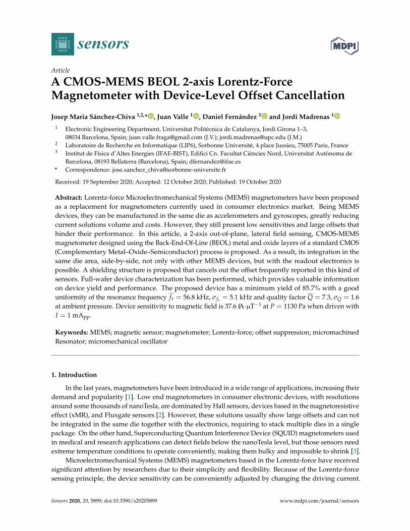
where I is the injected current,~L is the equivalent device length, and ~B is the magnetic field. When thiscurrent flows through a MEMS rotor, the resulting force generates an orthogonal displacement of themovable structure, as shown in the simplified MEMS diagram with the device electromechanical modelin Figure 1. Moreover, if the injected current is at the mechanical resonance frequency, so does theLorentz-force, resulting in an equivalent gap change Az described by [9,10]. In addition, Lorentz-forcemagnetometers are also usually driven electrostatically in order to sustain device oscillation when there isno magnetic field present. As a result, both the current and voltage driving generate a plate displacementdefined as
Az( fr) =Qk(FL + FE) ≈
Qk
(I · L · B + Vv
Cs
g
)(2)
where Q is the device quality factor, k is the spring stiffness, FE is the electrostatic force, V is the devicedc biasing voltage, v is the ac voltage or electrostatic driving, Cs is the device capacitance and g is thenominal gap. The effect of electrostatic driving has been included because, being a resonant device, it isof utmost importance to track the resonance frequency, which is usually done by placing the device in
Sensors 2020, 20, 5899 3 of 20
a self-sustained oscillation loop [9–14]. When there is no magnetic field, some amount of electrostaticdriving is required in order to keep the loop working correctly at resonance [14]. In this situation, when thecurrent and electrostatic drivings are in phase, the device works in amplitude modulation (AM), and theequivalent gap change in Equation (2) generates a change of the device capacitance that follows.
∆Cs = εrε0 A(
1g− 1
g− Az
)(3)
where εr = 1 is the air relative permittivity, ε0 ≈ 8.854 · 10−12F/m is the absolute permittivity, and A is theplate area.
Currentdriving
Electrostaticdriving
B
k
l
b
Rotor
Az g CS
StatorV
v
IDrive
Sense
Current path
Is
Figure 1. MEMS electromechanical model simplified diagram.
When the MEMS sensor has some amount of biasing voltage V and is driven with an ac current I,the gap variation generates a charge movement defined by is = dq(t)/dt
is ≈εrε0 AQVωr
g2k
(I · L · B︸ ︷︷ ︸Lorentz
+ VvCs
g︸ ︷︷ ︸Electrostatic
)(4)
where ωr is the device resonance angular frequency. The resulting device sensitivity is
Sis(B) =∂is
∂B=
εrε0 AQVωr ILg2k
(5)
Where it can be seen that sensitivity may be boosted by making the device area larger (increasingA and L) and softer (reducing k). Doing so, may reduce the need to increase the biasing voltage V anddriving current I.
Device characterization as a function of the output current for a given magnetic field is very usefulwhen a charge sensitive amplifier is used for the readout. However, given that the proposed device ischaracterized with an impedance analyser, a different approach must be used.
2.1. Device Characterization
MEMS measurements using the impedance analyser usually consist in measuring the deviceconductance (G) and susceptance (B) (or equivalent parameters), the real and imaginary parts of admittance
Sensors 2020, 20, 5899 4 of 20
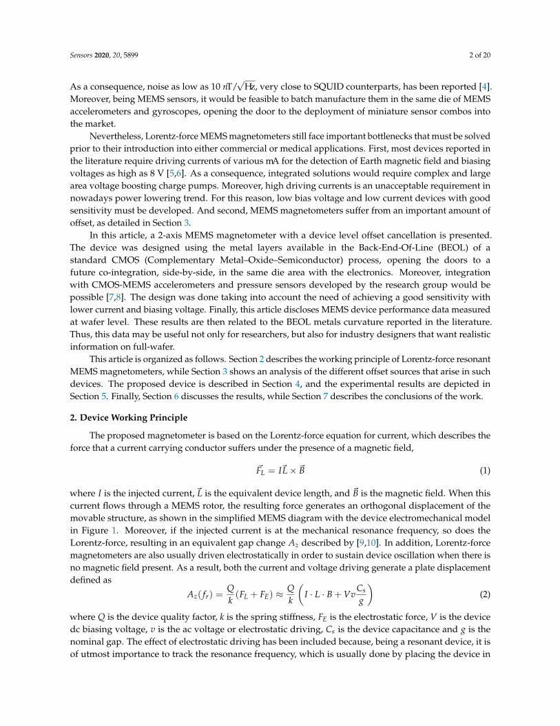
respectively. Doing so, it is possible to extract the MEMS mechanical parameters by using the second orderseries RLC resonator model, shown in Figure 2. The admittance of the model is
Y =R
R2 +(
ωL− 1ωC
)2
︸ ︷︷ ︸Conductance, G
+j
ωC0 +ωL− 1
ωC
R2 +(
ωL− 1ωC
)2
︸ ︷︷ ︸
Susceptance, B
(6)
where R, L, and C are the MEMS equivalent resonator components, C0 is the feedforward MEMScapacitance, and ω = 2π f is the angular frequency. A Python script has been coded that fits themeasurement data to the G model in Equation (6) and extracts the resonator RLC parameters usingthe least-squares minimization method. Then, MEMS resonance frequency fr, and quality factor Q can beextracted with
fr =1
2π
√1
LC(7)
Q =1R
√LC
(8)
C0
L R C
Figure 2. Second order RLC MEMS model used to fit the data.
At resonance, the L and C terms cancel each other out and, as a result, the conductance term inEquation (6) is equal to G( fr) = 1/R. Given that device output current expression in Equation (4) is anapproximation only valid at resonance frequency, it can be related to the conductance with
G( fr) =is
v=
εrε0 AQVωr
g2kv
(I · L · B + Vv
Cs
g
)(9)
whose sensitivity to magnetic field can be derived as
SG(B) =∂G( fr)
∂B=
εrε0 AQVωr ILg2kv
(10)
3. Offset Problems in Lorentz-Force Magnetometers: State of the Art
Lorentz-force MEMS magnetometers have numerous offset sources that limit their performance.The importance of these sources is strongly related to each device characteristics and topology.Nevertheless, they can be divided into two main categories: offset arising from voltage and offset arisingfrom current drivings. In the following subsection, the offset sources related to each type of driving areidentified and described.
Sensors 2020, 20, 5899 5 of 20
3.1. Offset Arising from Voltage Driving
Applying an ac voltage driving to the device generates two different offset sources: MEMS plateactuation and signal feedthrough.
1. Plate actuation is a consequence of the resulting electrostatic force between the MEMS statorand rotor when applying an ac voltage driving to the device. Such electrostatic force generatesa plate displacement that causes a gap change and a capacitance variation, as illustrated inEquations (2) and (3) respectively. In most AM Lorentz-force magnetometers, the electrostatic andcurrent drivings are usually applied with the same frequency and phase. While plate displacementdue to current driving (Lorentz-force) is desirable, displacement due to the electrostatic driving is anunwanted offset component. Such offset source is problematic as it reduces the dynamic range andhas been demonstrated to worsen the long term instability [5,9].
2. Signal feedthrough is an offset that arises when interfacing the MEMS device with the readoutelectronics. If the sensor is placed in a capacitive half Wheatstone bridge readout circuit amplifiedwith a fully-differential amplifier fed back with capacitors, the output signal vo as a function of thevoltage driving vi is
vo = vi∆CC f b
(11)
where C f b is the amplifier feedback capacitance and ∆C = Csensor−Cbridge is the capacitance differencebetween the sensor and the bridge capacitances. In differential sensors with ideal matching ∆C = 0this feedthrough is completely compensated. The same happens with capacitive bridges ideallymatched by using adjustable capacitors. However, MEMS capacitance drifts with temperature asa result of device springs coefficient change [15–17]. Moreover, MEMS capacitance may presentvariations due to fabrication and release non-idealities [18,19].
To avoid such offset sources, some works avoid the use of electrostatic driving: in [20,21] the sensorresonance frequency is tracked with resonators, but the sensing is performed at a frequency different fromresonance, a technique called off-resonance driving. As a result, perfect resonance frequency tracking isnot critical because the resulting sensitivity change at an offset frequency is minimized. Similarly, in [14],electrostatic driving is selectively enabled only when magnetic field is low enough to risk resonanceunlocking. Although the resulting electrostatic (Fe) and Lorentz (FL) forces are in quadrature, making itpossible to remove the electrostatic driving offset with a synchronous demodulation, non-idealities dueto this demodulation may arise, as well as capacitive bridge mismatch. To avoid that, in [9] complexmodulation and demodulation schemes are proposed that successfully remove the electrostatic drivingoffset component. However, offset due to the current feedthrough to the sense electrode, as will beexplained in the following subsection, can not be removed using this technique.
3.2. Offset Arising from Current Driving
There exist two types of offset sources related to the current driving: distributed electrostatic forcealong the current path, and capacitive coupling between the current path and sense node.
1. The fact that the resistance of the current carrying structure is not zero generates a voltage drop acrossthe MEMS current driving path. This voltage drop between the MEMS current source and sink istranslated into a distributed electrostatic force along the device that generates a plate displacement.Such issue is even worse in differential devices with current driven in series, as the resultingelectrostatic force suffers an important mismatch. Some works [21–23] propose the adjustment of thevoltage levels at these electrodes in order to compensate the mentioned electrostatic force imbalance.However, such solution requires manual adjustment, which is not feasible in mass production.
Sensors 2020, 20, 5899 6 of 20
2. There exists a parasitic capacitive coupling between the current carrying path and the sense node,which results in a current feedthrough directly to the device output. In Ref. [14], a capacitivenetwork between the current carrying path and the amplifier input is used to partly compensatethis offset source, similar to the solution proposed in Ref. [24]. In Ref. [5] this source of offset isremoved, together with other offset sources by using a complex modulation and demodulationstrategy. Unfortunately, the proposed complex circuit still presents some amount of offset due toimperfections of the implemented circuitry.
3.3. Total Offset
Output current in Equation (4) only takes into account the current generated by Lorentz-force andelectrostatic force plate displacements due to the device voltage driving. The former is the signal thatcarries magnetic field information, while the latter is the plate actuation offset source. However, it ispossible to further detail the output current by adding the offset due to capacitive coupling and non-zerocurrent path resistance
is ≈εrε0 AQVωr
g2k
(I · L · B + Vv
Cs
g+ Vvc
Cc
2g
)+ ωrCcvc (12)
where Cc is the capacitive coupling between the current path and sense node, and vc = I · Rcurrent is thevoltage applied to the current path, which is a function of the driving current I and the current pathresistance Rcurrent. Please note that capacitive coupling has been considered between current input andsense node, while plate displacement due to current driving has been considered to happen at the middleof the plate. Voltage feedthrough has not been included in Equation (12) because it appears only when thedevice is connected to a readout circuit, but it has already been depicted in Equation (11).
The offset removal proposed consists in shielding the current carrying path from the sense node,thus making Cc = 0 F. For this reason, it aims to cancel the offset arising from capacitive coupling. Moreover,as the current path is shielded, so does the equivalent electrostatic force due to the current driving. Hence,as a result of the shielding, the device output current is finally the one depicted in Equation (4).
4. Proposed Device
The proposed Lorentz-force MEMS magnetometer was designed and manufactured using the BEOLmetal and oxide layers of a 6-metal 180 nm CMOS process. Then, the MEMS structure was wafer levelreleased using vapour hydrofluoric acid (vHF), which etches away the oxide surrounding the MEMS,while keeping the structure metals and vias due to its high aluminium selectivity. The unmodifiedpassivation layer provided by the foundry was used as a mask to protect the rest of the die from the acid,while a passivation window was open to allow the acid to attack only the MEMS areas. A simplified crosssection diagram of the device and release process is shown in Figure 3a.
Sensors 2020, 20, 5899 7 of 20
Al metalW viaSiO2Si substrate
Si3N4 passivation
Drive electrodeCurrent path
Sense electrode
110.4 μm
11.4 μm
57
μm
57
μm
104 μm
10
4 μ
m
M5Current carrying path (M4)
(a) (b)
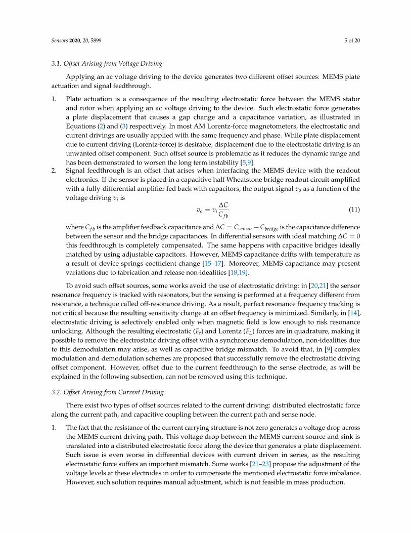
Figure 3. Device diagrams. In (a), simplified cross section diagram of the MEMS device manufacturedusing the BEOL layers of the CMOS process. On top, device at fab-out, below, after the release processwith the different device parts depicted. In (b), device diagram with dimensions. The top-most metal layer(M5) is shown in grey, while the vertical and horizontal current carrying paths (M4) are shown in red.Red arrows show the different current flow directions that allow magnetic field measurement in two axis.
The device is a single-ended, parallel plate device that resonates in the out-of-plane resonance mode.The plate rotor consists of a stack of M3–M5 metals kept together with long vias, which provide bothmechanical attachment and electrical connection between the different metal layers. Moreover, the use ofvarious metal and oxide layers stack reduces the plate curvature after oxide release [19,25–27]. In order toallow the release agent to penetrate the MEMS structure and release the oxide between the rotor and thestator, the MEMS plate has 3.56 µm×3.56 µm openings uniformly distributed across the plate. Total platedimensions are 104 µm×104 µm. A diagram of the MEMS device with its dimensions is provided inFigure 3b. Inside the plate, with M4, two 2.1 µm wide metal tracks cross the plate, from left to right and topto bottom, in a cross-like shape providing a low-resistance path to the driving current. These tracks crossone to each other in the middle of the plate, but they are electrically insulated from the rest of M3–M5 rotorstack with unreleased SiO2, as vHF does not penetrate the structure due to the isolation provided by themetal and via stacks. The rest of the plate is connected to the Drive electrode. Doing so, the current carryingpath is inside a Faraday cage-like structure that decouples the current from the Sense electrode. Due to itslow impedance at circuit level, the Drive electrode is used as a shield. As a result, the two current relatedoffset sources are avoided: first, there is no parasitic capacitance coupling between the current carryingpath and the sense node and, second, these nodes do no generate an electrostatic force distribution.
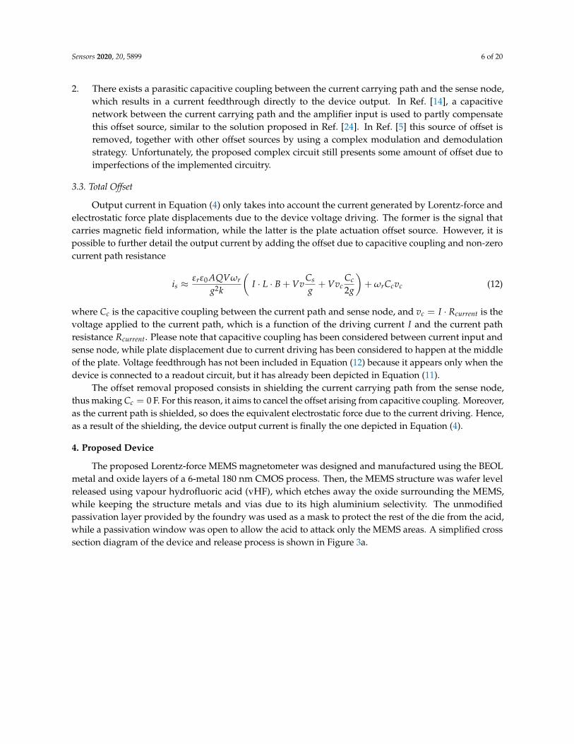
The device springs were designed with the same structure that the rest of the plate. The springcross-section diagram as well as a Focused Ion Beam (FIB) cut image are depicted in Figure 4. As aconsequence of the bulky cross-section of the springs, they were expected to have a relatively high stiffness.
Sensors 2020, 20, 5899 8 of 20
3.6 μm2.1 μm
M5
M4
M3
Al metal
W via
SiO2
V34
V45
Shield electrode
Current path
(a) (b)
Figure 4. Device spring cross-section diagram (a) and image after a Focused Ion Beam (FIB) cut (b). Same asthe rotor, the spring is made of a stack of M3–M5 metals and vias that surround the current carrying pathat M4.
The device stator is at M2, while M1 is used to connect the Sense electrode to the outside. The MEMSrotor is subjected to a frame that surrounds the entire device. This frame was designed as a stack of M1–M6metals and long vias that stop the penetration of the vHF and protect the surrounding MEMS devicesand electronics.
During the design, an important limitation was present: wafer level measurement setup requiredthe samples to be tested at ambient pressure. In order to be able to measure devices resonance in suchconditions, the final device springs had to be soft enough to provide a low restoring force easy to overcomeelectrostatically during the measurements. Moreover, soft springs also boost sensitivity, as deduced inEquations (5) and (10). For this reason, long springs were designed (110.4 µm between meanders) in orderto have a low stiffness coefficient. As a result of this design decision, the resonance frequency was lowered.Even though this fact simplified the device measurements and increased sensitivity, it must be taken intoaccount that very low resonance frequencies should be avoided in order to minimize the presence of flickernoise in the amplifying stage to maximize the Signal-to-Noise-Ratio (SNR).
Finally, distance between samples across the wafer is around 19.5 mm, and the proposed device isevenly replicated 56 times across a 8 inch wafer.
5. Experimental Results
In this section, the experimental measurements results are reported. However, in order to characterizethe proposed device, different measurements were performed, each one requiring a specific experimentalsetup. For this reason, in the first part of the section, the various setups used are described.
5.1. Measurement Setups
5.1.1. Wafer Level Batch Measurements
In order to understand the variations of the different device parameters across the wafer, wafer levelbatch measurements were performed. These measurements were carried out with probes using a MPITS2000 (MPI Corporation, Chu-pei, Taiwan) semi automatic probe machine. Using this setup and aKeysight 4990A (Keysight, Santa Rosa, CA, USA) impedance analyser, the following measurementswere performed:
• Drive to Sense capacitance and capacitance variation when sweeping the biasing voltage (C-V).
Sensors 2020, 20, 5899 9 of 20
• Resonance measurements at ambient pressure.• Current driving path resistance.• Current driving electrode to Sense node parasitic capacitive coupling.
5.1.2. Packaged Sample Vacuum Measurements
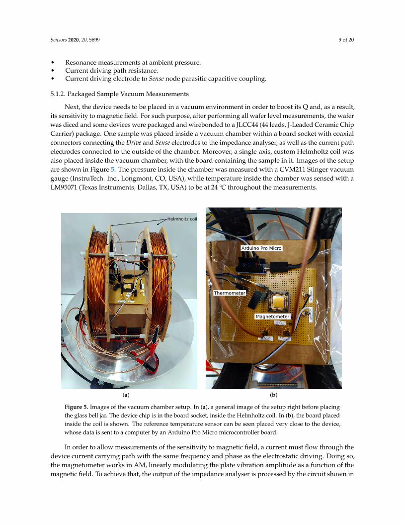
Next, the device needs to be placed in a vacuum environment in order to boost its Q and, as a result,its sensitivity to magnetic field. For such purpose, after performing all wafer level measurements, the waferwas diced and some devices were packaged and wirebonded to a JLCC44 (44 leads, J-Leaded Ceramic ChipCarrier) package. One sample was placed inside a vacuum chamber within a board socket with coaxialconnectors connecting the Drive and Sense electrodes to the impedance analyser, as well as the current pathelectrodes connected to the outside of the chamber. Moreover, a single-axis, custom Helmholtz coil wasalso placed inside the vacuum chamber, with the board containing the sample in it. Images of the setupare shown in Figure 5. The pressure inside the chamber was measured with a CVM211 Stinger vacuumgauge (InstruTech. Inc., Longmont, CO, USA), while temperature inside the chamber was sensed with aLM95071 (Texas Instruments, Dallas, TX, USA) to be at 24 C throughout the measurements.
Helmholtz coil
Arduino Pro Micro
Thermometer
Magnetometer
(a) (b)
Figure 5. Images of the vacuum chamber setup. In (a), a general image of the setup right before placingthe glass bell jar. The device chip is in the board socket, inside the Helmholtz coil. In (b), the board placedinside the coil is shown. The reference temperature sensor can be seen placed very close to the device,whose data is sent to a computer by an Arduino Pro Micro microcontroller board.
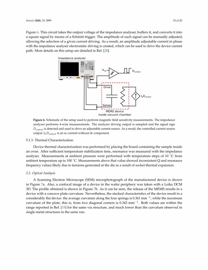
In order to allow measurements of the sensitivity to magnetic field, a current must flow through thedevice current carrying path with the same frequency and phase as the electrostatic driving. Doing so,the magnetometer works in AM, linearly modulating the plate vibration amplitude as a function of themagnetic field. To achieve that, the output of the impedance analyser is processed by the circuit shown in
Sensors 2020, 20, 5899 10 of 20
Figure 6. This circuit takes the output voltage of the impedance analyser, buffers it, and converts it intoa square signal by means of a Schmitt trigger. The amplitude of such signal can be manually adjusted,allowing the selection of a given current driving. As a result, an amplitude adjustable current in phasewith the impedance analyser electrostatic driving is created, which can be used to drive the device currentpath. More details on this setup are detailed in Ref. [28].
Impedance analyzer
Dcontrol
I0Dcontrol
MEMS deviceinside vacuum chamber
Vref
Drive
Sense
Figure 6. Schematic of the setup used to perform magnetic field sensitivity measurements. The impedanceanalyser performs 4-wire measurements. The analyser driving output is sampled and the signal signDcontrol is detected and used to drive an adjustable current source. As a result, the controlled current sourceoutput IODcontrol is an ac current without dc component.
5.1.3. Thermal Characterization
Device thermal characterization was performed by placing the board containing the sample insidean oven. After sufficient temperature stabilization time, resonance was measured with the impedanceanalyser. Measurements at ambient pressure were performed with temperature steps of 10 C fromambient temperature up to 100 C. Measurements above that value showed inconsistent Q and resonancefrequency values likely due to tensions generated at the die as a result of socket thermal expansion.
5.2. Optical Analysis
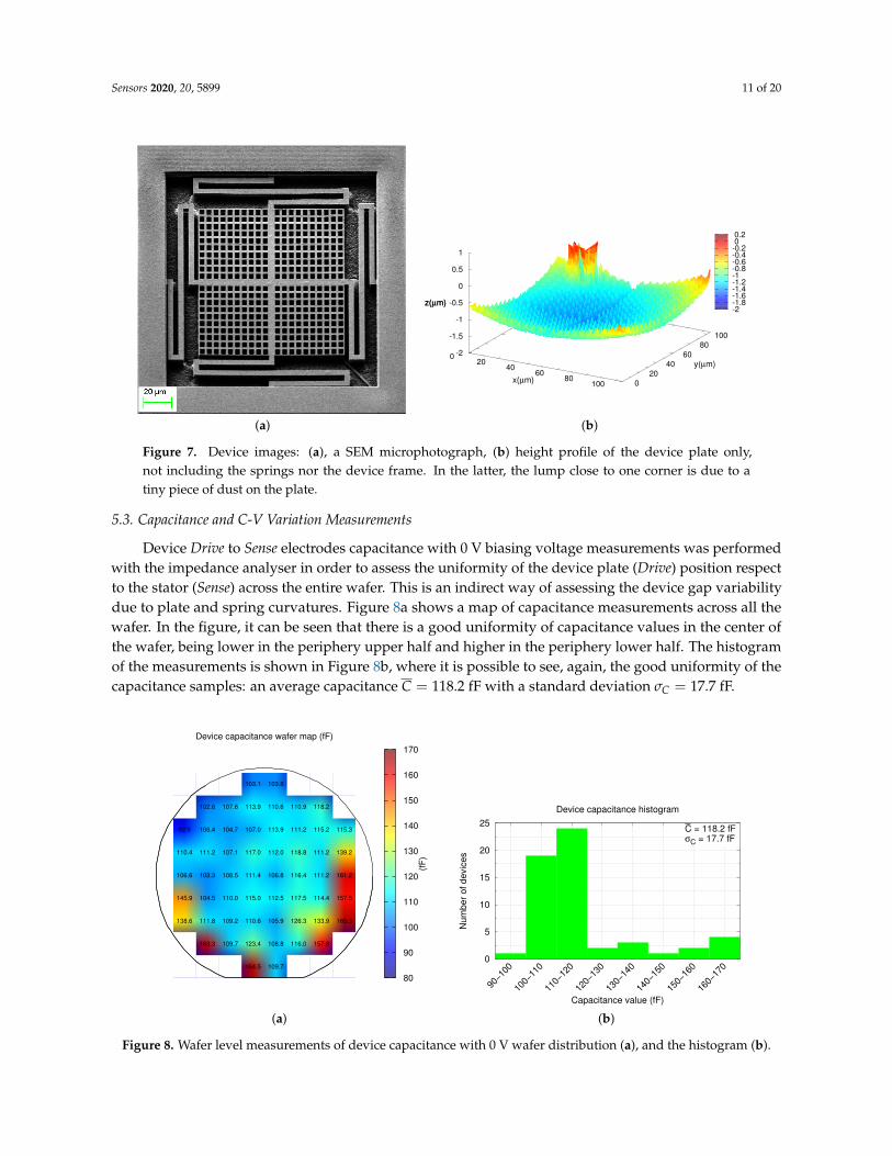
A Scanning Electron Microscope (SEM) microphotograph of the manufactured device is shownin Figure 7a. Also, a confocal image of a device in the wafer periphery was taken with a Leika DCM3D. The profile obtained is shown in Figure 7b. As it can be seen, the release of the MEMS results in adevice with a concave plate curvature. Nevertheless, the stacked characteristics of the device result in aconsiderably flat device: the average curvature along the four springs is 0.361 mm−1, while the maximumcurvature of the plate, this is, from two diagonal corners is 0.343 mm−1. Both values are within therange reported in Ref. [19] for the same via structure, and much lower than the curvature observed insingle-metal structures in the same run.
Sensors 2020, 20, 5899 11 of 20
0 20
40 60
80 100 0
20
40
60
80
100
-2
-1.5
-1
-0.5
0
0.5
1
z(µm)
x(µm)
y(µm)
z(µm)-2-1.8-1.6-1.4-1.2-1-0.8-0.6-0.4-0.2 0 0.2
(a) (b)
Figure 7. Device images: (a), a SEM microphotograph, (b) height profile of the device plate only,not including the springs nor the device frame. In the latter, the lump close to one corner is due to atiny piece of dust on the plate.
5.3. Capacitance and C-V Variation Measurements
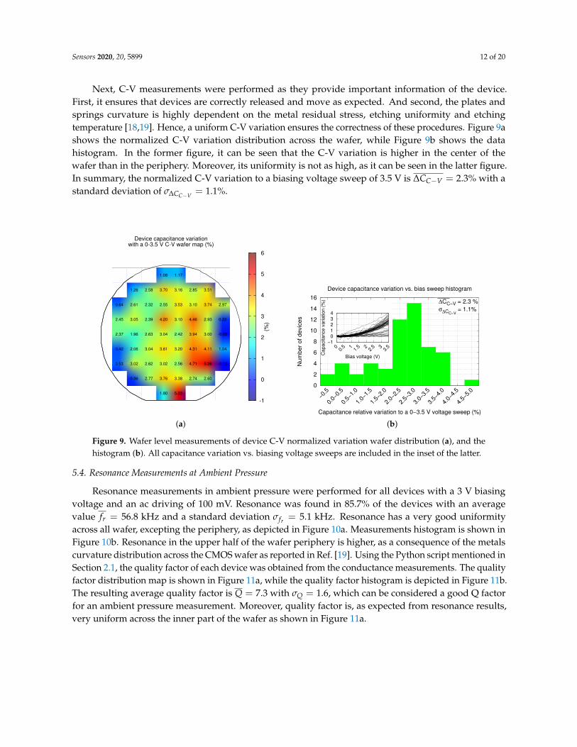
Device Drive to Sense electrodes capacitance with 0 V biasing voltage measurements was performedwith the impedance analyser in order to assess the uniformity of the device plate (Drive) position respectto the stator (Sense) across the entire wafer. This is an indirect way of assessing the device gap variabilitydue to plate and spring curvatures. Figure 8a shows a map of capacitance measurements across all thewafer. In the figure, it can be seen that there is a good uniformity of capacitance values in the center ofthe wafer, being lower in the periphery upper half and higher in the periphery lower half. The histogramof the measurements is shown in Figure 8b, where it is possible to see, again, the good uniformity of thecapacitance samples: an average capacitance C = 118.2 fF with a standard deviation σC = 17.7 fF.
Device capacitance wafer map (fF)
83.6 83.6 83.6 164.5 109.7 83.6 83.6 83.6
83.6 163.3 109.7 123.4 108.8 116.0 157.8 83.6
138.6 111.8 109.2 110.6 105.9 126.3 133.9 165.3
145.9 104.5 110.0 115.0 112.5 117.5 114.4 157.5
106.6 103.3 108.5 111.4 106.8 116.4 111.2 161.2
110.4 111.2 107.1 117.0 112.0 118.8 111.2 139.2
92.9 106.4 104.7 107.0 113.9 111.2 115.2 115.3
83.6 102.6 107.6 113.9 110.6 110.9 118.2 83.6
83.6 83.6 83.6 103.1 103.8 83.6 83.6 83.6
80
90
100
110
120
130
140
150
160
170
(fF
)
0
5
10
15
20
25
90−1
00
100−
110
110−
120
120−
130
130−
140
140−
150
150−
160
160−
170
Nu
mb
er
of
de
vic
es
Capacitance value (fF)
Device capacitance histogram
C = 118.2 fFσC = 17.7 fF
(a) (b)
Figure 8. Wafer level measurements of device capacitance with 0 V wafer distribution (a), and the histogram (b).
Sensors 2020, 20, 5899 12 of 20
Next, C-V measurements were performed as they provide important information of the device.First, it ensures that devices are correctly released and move as expected. And second, the plates andsprings curvature is highly dependent on the metal residual stress, etching uniformity and etchingtemperature [18,19]. Hence, a uniform C-V variation ensures the correctness of these procedures. Figure 9ashows the normalized C-V variation distribution across the wafer, while Figure 9b shows the datahistogram. In the former figure, it can be seen that the C-V variation is higher in the center of thewafer than in the periphery. Moreover, its uniformity is not as high, as it can be seen in the latter figure.In summary, the normalized C-V variation to a biasing voltage sweep of 3.5 V is ∆CC−V = 2.3% with astandard deviation of σ∆CC−V = 1.1%.
Device capacitance variationwith a 0-3.5 V C-V wafer map (%)
-0.11 -0.11 -0.11 1.80 5.23 -0.11 -0.11 -0.11
-0.11 0.36 2.77 3.76 3.38 2.74 2.60 -0.11
0.53 3.02 2.62 3.02 2.56 4.71 5.26 -0.12
0.42 2.06 3.04 3.61 3.20 4.31 4.11 1.04
2.37 1.96 2.63 3.04 2.42 3.94 3.00 -0.05
2.45 3.05 2.39 4.20 3.10 4.46 2.93 0.22
0.64 2.61 2.32 2.55 3.53 3.10 3.74 2.97
-0.11 1.26 2.58 3.70 3.16 2.85 3.51 -0.11
-0.11 -0.11 -0.11 1.08 1.17 -0.11 -0.11 -0.11
-1
0
1
2
3
4
5
6
(%)
0
2
4
6
8
10
12
14
16
−0.5
0.0−
0.5
0.5−
1.0
1.0−
1.5
1.5−
2.0
2.0−
2.5
2.5−
3.0
3.0−
3.5
3.5−
4.0
4.0−
4.5
4.5−
5.0
Nu
mb
er
of
de
vic
es
Capacitance relative variation to a 0−3.5 V voltage sweep (%)
Device capacitance variation vs. bias sweep histogram
∆CC−V = 2.3 %
σ∆CC−V
= 1.1%
−1 0 1 2 3 4
0 0
.5 1 1
.5 2 2
.5 3 3
.5
Capacitance v
ariation (
%)
Bias voltage (V)
(a) (b)
Figure 9. Wafer level measurements of device C-V normalized variation wafer distribution (a), and thehistogram (b). All capacitance variation vs. biasing voltage sweeps are included in the inset of the latter.
5.4. Resonance Measurements at Ambient Pressure
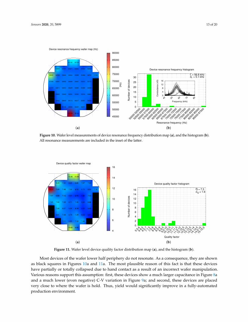
Resonance measurements in ambient pressure were performed for all devices with a 3 V biasingvoltage and an ac driving of 100 mV. Resonance was found in 85.7% of the devices with an averagevalue fr = 56.8 kHz and a standard deviation σfr = 5.1 kHz. Resonance has a very good uniformityacross all wafer, excepting the periphery, as depicted in Figure 10a. Measurements histogram is shown inFigure 10b. Resonance in the upper half of the wafer periphery is higher, as a consequence of the metalscurvature distribution across the CMOS wafer as reported in Ref. [19]. Using the Python script mentioned inSection 2.1, the quality factor of each device was obtained from the conductance measurements. The qualityfactor distribution map is shown in Figure 11a, while the quality factor histogram is depicted in Figure 11b.The resulting average quality factor is Q = 7.3 with σQ = 1.6, which can be considered a good Q factorfor an ambient pressure measurement. Moreover, quality factor is, as expected from resonance results,very uniform across the inner part of the wafer as shown in Figure 11a.
Sensors 2020, 20, 5899 13 of 20
Device resonance frequency wafer map (Hz)
47992 47992 47992 87178 55130 47992 47992 47992
47992 47992 55143 55093 56247 56221 53325 47992
47992 55402 55909 56113 56217 55697 54630 47992
47992 55885 55940 55291 55335 55218 55661 47992
54787 55811 56054 55629 55695 55382 56068 47992
57346 55551 55890 55495 55631 54910 55727 47992
69630 54704 55640 55922 55299 55496 54731 57590
47992 60894 54447 54371 54640 54542 56950 47992
47992 47992 47992 61132 60722 47992 47992 47992
45000
50000
55000
60000
65000
70000
75000
80000
85000
90000
(Hz)
0
5
10
15
20
25
30
5000
0-52
500
5250
0-55
000
5500
0-57
500
5750
0-60
000
6000
0-62
500
6250
0-65
000
6500
0-67
500
6750
0-70
000
7000
0-72
500
7250
0-75
000
7500
0-77
500
7750
0-80
000
8000
0-82
500
8250
0-85
000
8500
0-87
500
Nu
mb
er
of
de
vic
es
Resonance frequency (Hz)
Device resonance frequency histogram
fr = 56.8 kHzσfr
= 5.1 kHz
0
4
8
12
16
40 50 60 70 80
Conducta
nce (
nS
)
Frequency (kHz)
(a) (b)
Figure 10. Wafer level measurements of device resonance frequency distribution map (a), and the histogram (b).All resonance measurements are included in the inset of the latter.
Device quality factor wafer map
4.96 4.96 4.96 10.83 6.95 4.96 4.96 4.96
4.96 4.96 7.11 6.63 7.12 7.68 5.51 4.96
4.96 6.91 7.06 6.79 7.29 6.23 5.91 4.96
4.96 7.90 6.87 6.54 6.58 6.01 6.43 4.96
7.45 7.94 7.08 6.71 7.06 6.22 6.88 4.96
7.57 6.69 7.16 6.21 6.09 5.80 7.03 4.96
15.07 7.09 7.49 7.30 6.50 6.70 6.53 7.36
4.96 9.23 7.00 6.40 6.85 7.07 7.00 4.96
4.96 4.96 4.96 10.46 10.94 4.96 4.96 4.96
4
6
8
10
12
14
16
0
2
4
6
8
10
12
14
16
5,5-
6
6-6,
5
6,5-
7
7-7,
5
7,5-
8
8-8,
5
8,5-
9
9-9,
5
9,5-
10
10-1
0,5
10,5
-11
11-1
1,5
11,5
-12
12-1
2,5
12,5
-13
13-1
3,5
13,5
-14
14-1
4,5
14,5
-15
15-1
5,5
Nu
mb
er
of
de
vic
es
Quality factor
Device quality factor histogram
Q = 7.3σQ = 1.6
(a) (b)
Figure 11. Wafer level device quality factor distribution map (a), and the histogram (b).
Most devices of the wafer lower half periphery do not resonate. As a consequence, they are shownas black squares in Figures 10a and 11a. The most plausible reason of this fact is that these deviceshave partially or totally collapsed due to hand contact as a result of an incorrect wafer manipulation.Various reasons support this assumption: first, these devices show a much larger capacitance in Figure 8aand a much lower (even negative) C-V variation in Figure 9a; and second, these devices are placedvery close to where the wafer is hold. Thus, yield would significantly improve in a fully-automatedproduction environment.
Sensors 2020, 20, 5899 14 of 20
5.5. Current Driving to Sense Node Capacitive Coupling
The current driving path parasitic capacitance with the Sense node was also measured. The followedprocedure was: first, the probes were placed over the device pads and the impedance analyser parasiticcapacitance was calibrated; next, the probes for capacitance measurement were placed on the Senseelectrode and one of the inputs of current driving, contacting the pads, while the probe of Drive electrodewas connected to ground to provide the shielding. The measured parasitic capacitance coupling was,averaging all wafer samples, Ccoupling = 4.0 fF. This value is very low, thus it can be considered that theshielding works as expected. The low, non-zero measured value is thought to be a consequence of either(1) instrument calibration resolution and (2) probes or wires uncompensated stray capacitance due toposition change between calibration and probes making contact with the pads.
Finally, the minimum current path resistance measured is Rcurrent = 46.3 Ω, very close to the simulatedvalue of 45 Ω. The minimum measured value was considered as it is the one that provides the lower probeto pad contact resistance.
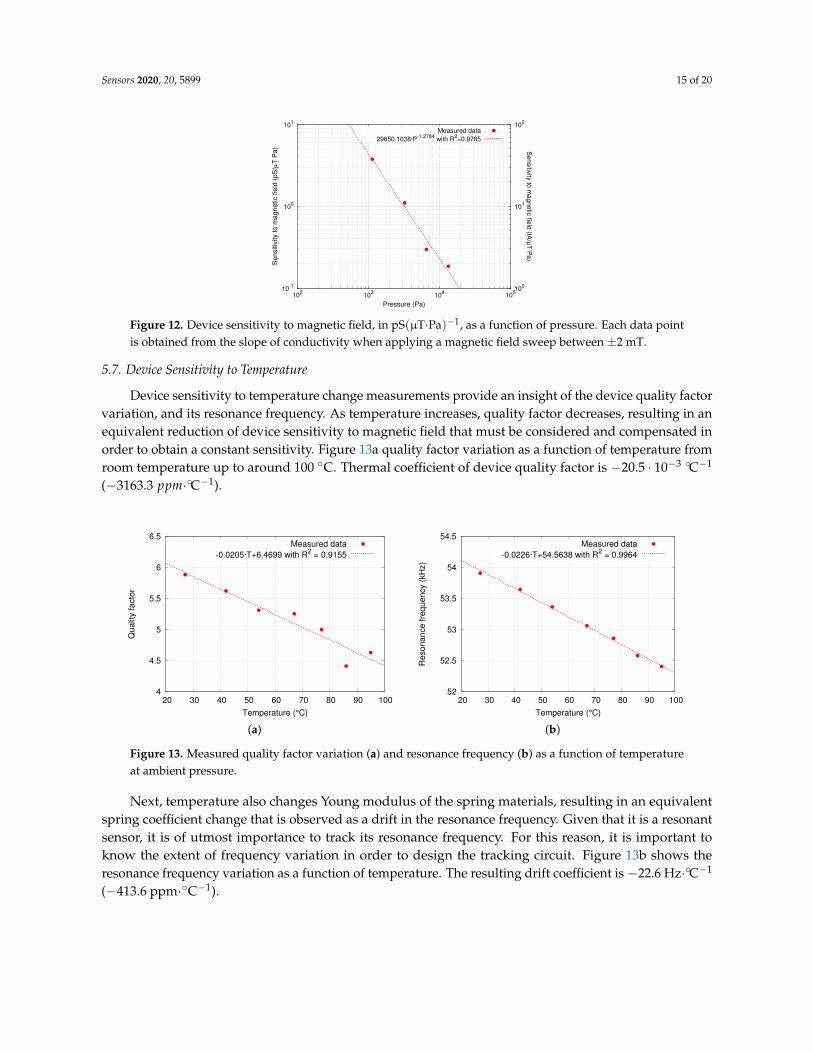
5.6. Device Sensitivity to Magnetic Field
As seen in Equation (10), device sensitivity to magnetic field is proportional to its Q, which is boostedat low pressure. For this reason, device sensitivity to magnetic field was measured at various pressurevalues in order to be able to assess the pressure at which the device may be packaged in a potentialcommercial solution. The measured device sensitivity to magnetic field as a function of the pressureis shown in Figure 12. Each sensitivity data point in the plot represents the conductance change as afunction of the applied magnetic field in pS·(µT·Pa)−1 units (left vertical axis). Such slope is obtainedfrom resonance measurements under the presence of a magnetic field sweep between ±2 mT with 320 µTsteps for each pressure value. As expected, the device sensitivity boosts at lower pressures following apower law relationship of
SG(B) = 29650.1 · P−1.2784 pSµT · Pa
(13)
for an electrostatic driving of v = 10 mV, a dc biasing of V = 1 V and a current of I = 1 mApp. Equation (13)is obtained from a power law fit. Unfortunately, at pressure lower than 600 Pa, the device starts to enter intoits nonlinear region with the mentioned electrostatic driving conditions. Lowering the ac driving voltage,linear measurements could be performed at lower pressures. Doing so, the packaging lower pressurelimit as well as the maximum sensitivity can be further extended. Combining Equations (9) and (10), it ispossible to see that device sensitivity in terms of output current can be expressed as
Sis(B) = SG(B) · v (14)
where v is the electrostatic driving voltage, a term that modulates the measured sensitivity in Equation (13),but that cancels out in Equation (14) with the v in the denominator of Equation (9). Sensitivity in terms ofoutput current is also included in Figure 12 as seen in current units of fA·(µT·Pa)−1 (right vertical axis).
Sensors 2020, 20, 5899 15 of 20
10-1
100
101
102
103
104
10510
0
101
102
Sensitiv
ity to m
agnetic fie
ld (
pS
/µT
Pa) S
en
sitiv
ity to
ma
gn
etic
field
(fA/µ
T P
a)
Pressure (Pa)
Measured data
29650.1038·P-1.2784
with R2=0.9785
Figure 12. Device sensitivity to magnetic field, in pS(µT·Pa)−1, as a function of pressure. Each data pointis obtained from the slope of conductivity when applying a magnetic field sweep between ±2 mT.
5.7. Device Sensitivity to Temperature
Device sensitivity to temperature change measurements provide an insight of the device quality factorvariation, and its resonance frequency. As temperature increases, quality factor decreases, resulting in anequivalent reduction of device sensitivity to magnetic field that must be considered and compensated inorder to obtain a constant sensitivity. Figure 13a quality factor variation as a function of temperature fromroom temperature up to around 100 C. Thermal coefficient of device quality factor is −20.5 · 10−3 C−1
(−3163.3 ppm·C−1).
4
4.5
5
5.5
6
6.5
20 30 40 50 60 70 80 90 100
Qu
alit
y f
acto
r
Temperature (°C)
Measured data
-0.0205·T+6.4699 with R2 = 0.9155
52
52.5
53
53.5
54
54.5
20 30 40 50 60 70 80 90 100
Re
so
na
nce
fre
qu
en
cy (
kH
z)
Temperature (°C)
Measured data
-0.0226·T+54.5638 with R2 = 0.9964
(a) (b)
Figure 13. Measured quality factor variation (a) and resonance frequency (b) as a function of temperatureat ambient pressure.
Next, temperature also changes Young modulus of the spring materials, resulting in an equivalentspring coefficient change that is observed as a drift in the resonance frequency. Given that it is a resonantsensor, it is of utmost importance to track its resonance frequency. For this reason, it is important toknow the extent of frequency variation in order to design the tracking circuit. Figure 13b shows theresonance frequency variation as a function of temperature. The resulting drift coefficient is −22.6 Hz·C−1
(−413.6 ppm·C−1).
Sensors 2020, 20, 5899 16 of 20
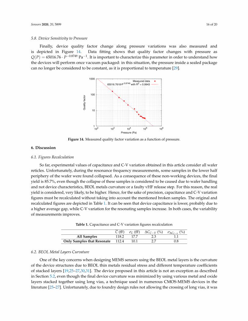
5.8. Device Sensitivity to Pressure
Finally, device quality factor change along pressure variations was also measured andis depicted in Figure 14. Data fitting shows that quality factor changes with pressure asQ(P) = 65016.76 · P−0.8749 Pa−1. It is important to characterize this parameter in order to understand howthe devices will perform once vacuum packaged: in this situation, the pressure inside a sealed packagecan no longer be considered to be constant, as it is proportional to temperature [29].
1
10
100
1000
102
103
104
105
106
Qu
alit
y f
acto
r
Pressure (Pa)
Measured data
65016.7618·P-0.8749
with R2 = 0.9943
Figure 14. Measured quality factor variation as a function of pressure.
6. Discussion
6.1. Figures Recalculation
So far, experimental values of capacitance and C-V variation obtained in this article consider all waferreticles. Unfortunately, during the resonance frequency measurements, some samples in the lower halfperiphery of the wafer were found collapsed. As a consequence of these non-working devices, the finalyield is 85.7%, even though the collapse of these samples is considered to be caused due to wafer handlingand not device characteristics, BEOL metals curvature or a faulty vHF release step. For this reason, the realyield is considered, very likely, to be higher. Hence, for the sake of precision, capacitance and C-V variationfigures must be recalculated without taking into account the mentioned broken samples. The original andrecalculated figures are depicted in Table 1. It can be seen that device capacitance is lower, probably due toa higher average gap, while C-V variation for the resonating samples increase. In both cases, the variabilityof measurements improves.
Table 1. Capacitance and C-V variation figures recalculation
C (fF) σC (fF) ∆CC−V (%) σ∆CC−V (%)All Samples 118.2 17.7 2.3 1.1
Only Samples that Resonate 112.4 10.1 2.7 0.8
6.2. BEOL Metal Layers Curvature
One of the key concerns when designing MEMS sensors using the BEOL metal layers is the curvatureof the device structures due to BEOL thin metals residual stress and different temperature coefficientsof stacked layers [19,25–27,30,31]. The device proposed in this article is not an exception as describedin Section 5.2, even though the final device curvature was minimized by using various metal and oxidelayers stacked together using long vias, a technique used in numerous CMOS-MEMS devices in theliterature [25–27]. Unfortunately, due to foundry design rules not allowing the crossing of long vias, it was
Sensors 2020, 20, 5899 17 of 20
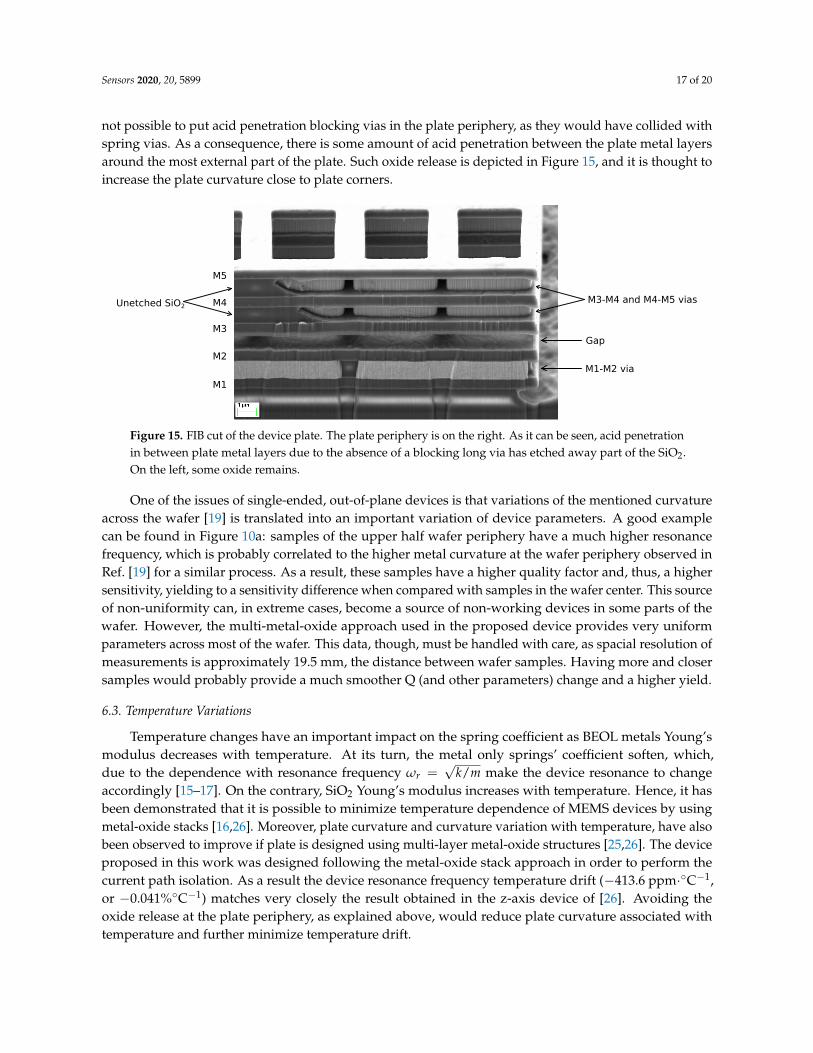
not possible to put acid penetration blocking vias in the plate periphery, as they would have collided withspring vias. As a consequence, there is some amount of acid penetration between the plate metal layersaround the most external part of the plate. Such oxide release is depicted in Figure 15, and it is thought toincrease the plate curvature close to plate corners.
Unetched SiO2
M1
M2
M3
M4
M5
Gap
M3-M4 and M4-M5 vias
M1-M2 via
Figure 15. FIB cut of the device plate. The plate periphery is on the right. As it can be seen, acid penetrationin between plate metal layers due to the absence of a blocking long via has etched away part of the SiO2.On the left, some oxide remains.
One of the issues of single-ended, out-of-plane devices is that variations of the mentioned curvatureacross the wafer [19] is translated into an important variation of device parameters. A good examplecan be found in Figure 10a: samples of the upper half wafer periphery have a much higher resonancefrequency, which is probably correlated to the higher metal curvature at the wafer periphery observed inRef. [19] for a similar process. As a result, these samples have a higher quality factor and, thus, a highersensitivity, yielding to a sensitivity difference when compared with samples in the wafer center. This sourceof non-uniformity can, in extreme cases, become a source of non-working devices in some parts of thewafer. However, the multi-metal-oxide approach used in the proposed device provides very uniformparameters across most of the wafer. This data, though, must be handled with care, as spacial resolution ofmeasurements is approximately 19.5 mm, the distance between wafer samples. Having more and closersamples would probably provide a much smoother Q (and other parameters) change and a higher yield.
6.3. Temperature Variations
Temperature changes have an important impact on the spring coefficient as BEOL metals Young’smodulus decreases with temperature. At its turn, the metal only springs’ coefficient soften, which,due to the dependence with resonance frequency ωr =
√k/m make the device resonance to change
accordingly [15–17]. On the contrary, SiO2 Young’s modulus increases with temperature. Hence, it hasbeen demonstrated that it is possible to minimize temperature dependence of MEMS devices by usingmetal-oxide stacks [16,26]. Moreover, plate curvature and curvature variation with temperature, have alsobeen observed to improve if plate is designed using multi-layer metal-oxide structures [25,26]. The deviceproposed in this work was designed following the metal-oxide stack approach in order to perform thecurrent path isolation. As a result the device resonance frequency temperature drift (−413.6 ppm·C−1,or −0.041%C−1) matches very closely the result obtained in the z-axis device of [26]. Avoiding theoxide release at the plate periphery, as explained above, would reduce plate curvature associated withtemperature and further minimize temperature drift.
Sensors 2020, 20, 5899 18 of 20
In order to minimize these variations even further, differential devices are usually used, as theycompensate temperature and process variations to the first order [32]. Moreover, different gap distancesmay be compensated, in differential devices, by applying an electrostatic force that minimizes suchdifference. Some strategies to convert the proposed single-ended device to a differential one are to make itwork in the torsional or lateral resonance modes and implement the detection capacitance with fingers inthe device sides. However, the most straightforward strategy may be covering the device with a metallayer that, together with the M1 stator and the plate, would make up the differential device. In that case,some precautions must be taken into account. First, rotor to top and bottom stators capacitance must bematched during the design stage. Second, holes must be included in the top electrode in order to allow theacid to penetrate and release the structure. Third, expected rotor curvature must be taken into account inorder to avoid the plate to collapse with any of the two stator layers. And fourth, the release step must becarefully performed in order to avoid stiction with the new layer.
7. Conclusions
In this article, an out-of-plane, lateral field sensing, 2-axis CMOS-MEMS magnetometer designedwith the BEOL metal layers of a standard CMOS process is proposed. Designing the device using suchmaterials, it is possible to manufacture it next to the electronics, side-by-side on the same die, which wouldallow the further shrink integrated sensing solutions based on MEMS sensors, as well as improvingthe yield an reducing the manufacturing cost. The device provides complete cancellation of offsets atdevice level, which is one of the main concerns of Lorentz-force MEMS magnetometers as offset hasbeen reported to reduce dynamic range and worsen long terms instability. The cancellation is performedby placing the current carrying path inside the plate structure, which completely shields the currentelectrode and insulates it in a Faraday cage-like structure connected to the low impedance Drive electrode.The current path isolation has been demonstrated by measuring the capacitance between the current andthe sensing electrode. Device integration with the readout electronics, though, is expected to providefurther measurements validating such solution. Some device experimental measurements were performedat wafer level, which provides data on the performance of the proposed device across all the wafer. Hence,wafer level measurements of device capacitance, C-V variation, resonance frequency, and quality factorwere performed, whose results have been related to previous literature on the topic of BEOL metallizationcurvatures for similar processes. Concretely, it has been demonstrated that multi-layer stacking techniquespreviously used to minimize plate curvature provide excellent results when it comes to device parametersscattering. Moreover, sensitivity to magnetic field as a function of pressure has been measured to evaluatethe lowest package pressure that would provide the highest sensitivity before driving the device into itsnon-linear operating region proving that the device is capable to work in the linear regime down to verylow pressure. Finally, device resonance frequency temperature dependence was measured, as well asdevice quality factor variation, which gives an interesting glance on how much device sensitivity driftswith temperature. Such figure is an important parameter to know given the current commercial andautomotive demanding temperature specifications.
Author Contributions: Conceptualization, J.V. and D.F.; Shield concept, J.V.; Funding acquisition, J.M.; Investigation,J.M.S.-C.; Methodology, J.M.S.-C., D.F.; Project administration, J.M.; Resources, J.M.; Supervision, D.F. and J.M.;Visualization, J.M.S.-C.; Writing original draft, J.M.S.-C.; and Writing review and editing, J.V., D.F., J.M. All authorshave read and agreed to the published version of the manuscript
Funding: This research was supported in part under project RTI2018-099766-B-I00 by the Spanish Ministry of Science,Innovation and Universities, the State Research Agency (AEI), and the European Social Fund (ESF).
Acknowledgments: The authors would like to acknowledge Alba Martínez for taking the confocal microscope andSEM images, Piotr Michalik for his help with the semi-automatic probe machine measurements, and Josep Àngel Oltrafor his assistance with the semi-automatic probe machine and for conducting high-voltage stress tests to the device.
Sensors 2020, 20, 5899 19 of 20
Conflicts of Interest: The authors declare no conflict of interest. The founding sponsors had no role in the design ofthe study; in the collection, analyses, or interpretation of data; in the writing of the manuscript, and in the decision topublish the results.
References
1. Magnetic Sensor. Market and Technology Report-November 2017; Technical Report; Yole Développement:Villeurbanne, France, 2017.
2. Lahrach, A. eCompass Comparative Report; Technical Report; System Plus Consulting: Nantes, France, 2015.3. Lenz, J.; Edelstein, S. Magnetic sensors and their applications. IEEE Sens J. 2006, 6, 631–649. [CrossRef]4. Kyynäräinen, J.; Saarilahti, J.; Kattelus, H.; Kärkkäinen, A.; Meinander, T.; Oja, A.; Pekko, P.; Seppä, H.; Suhonen,
M.; Kuisma, H.; et al. A 3D micromechanical compass. Sens. Actuators A 2008, 142, 561–568. [CrossRef]5. Sonmezoglu, S.; Horsley, D.A. Reducing Offset and Bias Instability in Lorentz Force Magnetic Sensors Through
Bias Chopping. J. Microelectromech. Syst. 2017, 26, 169–178. [CrossRef]6. Ghosh, S.; Lee, J.E. Eleventh Order Lamb Wave Mode Biconvex Piezoelectric Lorentz Force Magnetometer for
Scaling Up Responsivity and Bandwidth. In Proceedings of the 20th International Conference on Solid-StateSensors, Actuators and Microsystems Eurosensors XXXIII (TRANSDUCERS EUROSENSORS XXXIII), Berlin,Germany, 23–27 June 2019; pp. 146–149.
7. Michalik, P.; Sánchez-Chiva, J.M.; Fernández, D.; Madrenas, J. CMOS BEOL-embedded z-axis accelerometer.Electron. Lett 2015, 51, 865–867. [CrossRef]
8. Banerji, S.; Fernández, D.; Madrenas, J. Characterization of CMOS-MEMS Resonant Pressure Sensors.IEEE Sens. J. 2017, 17, 6653–6661. [CrossRef]
9. Li, M.; Horsley, D.A. Offset Suppression in a Micromachined Lorentz Force Magnetic Sensor by CurrentChopping. J. Microelectromech. Syst. 2014, 23, 1477–1484.
10. Li, M.; Sonmezoglu, S.; Horsley, D.A. Extended Bandwidth Lorentz Force Magnetometer Based on QuadratureFrequency Modulation. J. Microelectromech. Syst. 2015, 24, 333–342. [CrossRef]
11. Sunier, R.; Vancura, T.; Li, Y.; Kirstein, K.; Baltes, H.; Brand, O. Resonant Magnetic Field Sensor With FrequencyOutput. J. Microelectromech. Syst. 2006, 15, 1098–1107. [CrossRef]
12. Bahreyni, B.; Shafai, C. A Resonant Micromachined Magnetic Field Sensor. IEEE Sens. J. 2007, 7, 1326–1334.[CrossRef]
13. Li, M.; Ng, E.J.; Hong, V.A.; Ahn, C.H.; Yang, Y.; Kenny, T.W.; Horsley, D.A. Lorentz force magnetometer using amicromechanical oscillator. Appl. Phys. Lett. 2013, 103, 173504. [CrossRef]
14. Sánchez-Chiva, J.M.; Valle, J.; Fernández, D.; Madrenas, J. A Mixed-Signal Control System for Lorentz-ForceResonant MEMS Magnetometers. IEEE Sens. J. 2019, 19, 7479–7488. [CrossRef]
15. Hsu, W.T.; Nguyen, C.T. Stiffness-compensated temperature-insensitive micromechanical resonators.In Proceedings of the fifteenth IEEE International Conference on Micro Electro Mechanical Systems, Las Vegas,NV, USA, 24 January 2002; pp. 731–734.
16. Chen, W.C.; Fang, W.; Li, S.S. A generalized CMOS-MEMS platform for micromechanical resonatorsmonolithically integrated with circuits. J. Microelectromech. Syst. 2011, 21, 065012. [CrossRef]
17. Jan, M.T.; Ahmad, F.; Hamid, N.H.B.; Khir, M.H.B.M.; Shoaib, M.; Ashraf, K. Temperature dependentYoung’s modulus and quality factor of CMOS-MEMS resonator: Modelling and experimental approach.Microelectron. Reliab. 2016, 57, 64–70. [CrossRef]
18. Valle, J.; Fernández, D.; Madrenas, J. Experimental Analysis of Vapor HF Etch Rate and Its Wafer Level Uniformityon a CMOS-MEMS Process. J. Microelectromech. Syst. 2016, 25, 401–412. [CrossRef]
19. Valle, J.; Fernández, D.; Madrenas, J.; Barrachina, L. Curvature of BEOL Cantilevers in CMOS-MEMS Processes.J. Microelectromech. Syst. 2017, 26, 895–909. [CrossRef]
20. Minotti, P.; Brenna, S.; Laghi, G.; Bonfanti, A.G.; Langfelder, G.; Lacaita, A.L. A Sub-400-nT/√
Hz, 775-µW,Multi-Loop MEMS Magnetometer With Integrated Readout Electronics. J. Microelectromech. Syst. 2015,24, 1938–1950. [CrossRef]
Sensors 2020, 20, 5899 20 of 20
21. Laghi, G.; Marra, C.R.; Minotti, P.; Tocchio, A.; Langfelder, G. A 3-D Micromechanical Multi-Loop MagnetometerDriven Off-Resonance by an On-Chip Resonator. J. Microelectromech. Syst. 2016, 25, 637–651. [CrossRef]
22. Thompson, M.J.; Horsley, D.A. Parametrically Amplified Z-Axis Lorentz Force Magnetometer.J. Microelectromech. Syst. 2011, 20, 702–710. [CrossRef]
23. Li, M.; Rouf, V.T.; Thompson, M.J.; Horsley, D.A. Three-Axis Lorentz-Force Magnetic Sensor for ElectronicCompass Applications. J. Microelectromech. Syst. 2012, 21, 1002–1010. [CrossRef]
24. Lee, J.Y.; Seshia, A. Parasitic feedthrough cancellation techniques for enhanced electrical characterization ofelectrostatic microresonators. Sens. Actuators A 2009, 156, 36–42. [CrossRef]
25. Yen, T.; Tsai, M.; Chang, C.; Liu, Y.; Li, S.; Chen, R.; Chiou, J.; Fang, W. Improvement of CMOS-MEMSaccelerometer using the symmetric layers stacking design. In Proceedings of the SENSORS, 2011 IEEE, Limerick,Ireland, 28–31 October 2011; pp. 145–148.
26. Tsai, M.; Liu, Y.; Liang, K.; Fang, W. Monolithic CMOS-MEMS Pure Oxide Tri-Axis Accelerometers forTemperature Stabilization and Performance Enhancement. J. Microelectromech. Syst. 2015, 24, 1916–1927.[CrossRef]
27. Michalik, P.; Fernández, D.; Wietstruck, M.; Kaynak, M.; Madrenas, J. Experiments on MEMS Integration in 0.25µm CMOS Process. Sensors 2018, 18, 2111. [CrossRef] [PubMed]
28. Sánchez-Chiva, J.M.; Fernández, D.; Madrenas, J. A test setup for the characterization of Lorentz-force MEMSmagnetometers. In Proceedings of the 27th IEEE International Conference on Electronics, Circuits and Systems(ICECS), Glasgow, Scotland, 23–25 November 2020; accepted as presentation.
29. Kim, B.; Hopcroft, M.A.; Candler, R.N.; Jha, C.M.; Agarwal, M.; Melamud, R.; Chandorkar, S.A.; Yama, G.;Kenny, T.W. Temperature Dependence of Quality Factor in MEMS Resonators. J. Microelectromech. Syst. 2008,17, 755–766. [CrossRef]
30. Downey, R.H.; Karunasiri, G. Reduced Residual Stress Curvature and Branched Comb Fingers IncreaseSensitivity of MEMS Acoustic Sensor. J. Microelectromech. Syst. 2014, 23, 417–423. [CrossRef]
31. Cheng, C.L.; Tsai, M.H.; Fang, W. Determining the thermal expansion coefficient of thin films for a CMOS MEMSprocess using test cantilevers. J. Microelectromech. Syst. 2015, 25. [CrossRef]
32. Buffa, C. MEMS Lorentz Force Magnetometers; Springer: Cham, Switzerland, 2017; p. 55.
Publisher’s Note: MDPI stays neutral with regard to jurisdictional claims in published maps and institutionalaffiliations.
© 2020 by the authors. Licensee MDPI, Basel, Switzerland. This article is an open access articledistributed under the terms and conditions of the Creative Commons Attribution (CC BY)license (http://creativecommons.org/licenses/by/4.0/).