universal mechanical exfoliation of large-area 2d crystalselemental two-dimensional crystals,...
TRANSCRIPT
ARTICLE
Universal mechanical exfoliation of large-area 2DcrystalsYuan Huang1,2,12, Yu-Hao Pan3,12, Rong Yang1,2,12, Li-Hong Bao 1, Lei Meng1, Hai-Lan Luo 1, Yong-Qing Cai1,
Guo-Dong Liu1, Wen-Juan Zhao1, Zhang Zhou1, Liang-Mei Wu1, Zhi-Li Zhu1, Ming Huang 4, Li-Wei Liu5,
Lei Liu 6, Peng Cheng1, Ke-Hui Wu1, Shi-Bing Tian1, Chang-Zhi Gu 1, You-Guo Shi1, Yan-Feng Guo7,
Zhi Gang Cheng 1,2,8, Jiang-Ping Hu1,2,8, Lin Zhao1,2,8, Guan-Hua Yang9, Eli Sutter 10, Peter Sutter 11✉,
Ye-Liang Wang1,4, Wei Ji 2✉, Xing-Jiang Zhou1,2,8✉ & Hong-Jun Gao 1,8✉
Two-dimensional materials provide extraordinary opportunities for exploring phenomena
arising in atomically thin crystals. Beginning with the first isolation of graphene, mechanical
exfoliation has been a key to provide high-quality two-dimensional materials, but despite
improvements it is still limited in yield, lateral size and contamination. Here we introduce a
contamination-free, one-step and universal Au-assisted mechanical exfoliation method and
demonstrate its effectiveness by isolating 40 types of single-crystalline monolayers, including
elemental two-dimensional crystals, metal-dichalcogenides, magnets and superconductors.
Most of them are of millimeter-size and high-quality, as shown by transfer-free measure-
ments of electron microscopy, photo spectroscopies and electrical transport. Large sus-
pended two-dimensional crystals and heterojunctions were also prepared with high-yield.
Enhanced adhesion between the crystals and the substrates enables such efficient exfoliation,
for which we identify a gold-assisted exfoliation method that underpins a universal route for
producing large-area monolayers and thus supports studies of fundamental properties and
potential application of two-dimensional materials.
https://doi.org/10.1038/s41467-020-16266-w OPEN
1 Institute of Physics, Chinese Academy of Sciences, 100190 Beijing, China. 2 Songshan Lake Materials Laboratory, 523808 Dongguan, China. 3 Department ofPhysics and Beijing Key Laboratory of Optoelectronic Functional Materials & Micro-Nano Devices, Renmin University of China, 100872 Beijing, China.4 School of Materials Science and Engineering, Ulsan National Institute of Science and Technology (UNIST), Ulsan 44919, Republic of Korea. 5 School ofInformation and Electronics, MIIT Key Laboratory for Low-Dimensional Quantum Structure and Devices, Beijing Institute of Technology, 100081Beijing, China. 6 College of Engineering, Peking University, 100871 Beijing, China. 7 School of Physical Science and Technology, Shanghai Tech University,201210 Shanghai, China. 8 University of Chinese Academy of Sciences, 100049 Beijing, China. 9 Institute of Microelectronics of Chinese Academy ofSciences, 100029 Beijing, China. 10 Department of Mechanical and Materials Engineering, University of Nebraska—Lincoln, Lincoln, NE 68588, United States.11 Department of Electrical and Computer Engineering, University of Nebraska—Lincoln, Lincoln, NE 68588, United States. 12These authors contributedequally: Yuan Huang, Yu-Hao Pan, Rong Yang. ✉email: [email protected]; [email protected]; [email protected]; [email protected]
NATURE COMMUNICATIONS | (2020) 11:2453 | https://doi.org/10.1038/s41467-020-16266-w |www.nature.com/naturecommunications 1
1234
5678
90():,;
Two-dimensional (2D) materials continue to revealdimensionality-correlated quantum phenomena1–6, suchas 2D superconductivity, magnetism, topologically pro-
tected states, and quantum transport1,7–11. Stacking 2D materialsinto van der Waals heterostructures leads to further emergentphenomena and derived device concepts12,13. The further dis-covery and application of their properties depend on the devel-opment of synthesis strategies for 2D materials andheterostructures6,14–18. Synthesis using crystal growth methodscan now produce large (millimeter scale) single crystals of some2D materials, notably graphene and hexagonal boron nitride, butthe scalable growth of high-quality crystals has remained chal-lenging18,19, with many 2D materials and especially hetero-structures proving difficult to realize by bottom-up approaches.Ion-intercalation and liquid exfoliation are used as top-downapproaches but, as chemical methods, they often cause con-tamination of the isolated 2D surfaces20,21. While some gold-assisted exfoliation methods were demonstrated in layered chal-cogenides22–24, those methods still bring unexpected con-tamination in samples prepared for electrical and opticalmeasurements and thus reduce their performances whenremoving gold films with chemical solvents in additional steps. Inlight of this, a contamination-free, one-step and universal pre-paration strategy for large-area, high-quality monolayer materialsis still lacking for both fundamental research and applications.
In the past 15 years, mechanical exfoliation has been a uniqueenabler of the exploration of emergent 2D materials. Mostintrinsic properties of graphene, such as the quantum Halleffect25, massless Dirac Fermions26, and superconductivity27,were mostly observed on exfoliated flakes but are either inac-cessible or suppressed in samples prepared by other methods17,28.While exfoliation often suffers from low yield and small sizes ofthe exfoliated 2D flakes5, many layered materials are, however,yet to be exfoliated into monolayers by established exfoliationmethods. Such challenge of exfoliation limits their utility forscalable production of 2D crystals and complicates further pro-cessing, e.g., to fabricate heterostructures. These issues could beresolved by identifying suitable substrates that firmly adhere to2D crystals without compromising their structure and properties,thus allowing the separation and transfer of the entire top sheetfrom a layered bulk crystal. Covalent-like quasi-bonding (CLQB),a recently uncovered non-covalent interaction with typicalinteraction energies of ~0.5 eV per unit cell29–31, fits therequirements of the craving interaction between substrates and2D layers. The intermediate interaction energy for CLQB is abalance of a reasonably large Pauli repulsion induced by inter-layer wavefunction overlap and an enhanced dispersion attractioncaused by more pronounced electron correlation in 2D layerswith high polarizability.
Promising candidate substrates for CLQB with 2D crystals arematerials whose Fermi level falls in a partially filled band withmostly s- or p-electrons to prevent disrupting the electronicstructure of 2D layers, and which have highly polarizable electrondensities to ensure a large dispersion attraction. Noble metalsmeet these criteria and are easily obtained as clean solid surfaces.Group 11 (IB) coinage metals, i.e., Cu, Ag, and Au, remain aspotential candidates after ruling out group 8–10 (VIII) metals oftoo strong hybridization, Al of high activity to 2D layers and inair32,33 and closed-shell group 12 (IIB) metals (Zn, Cd, Hg).Among those three, Au interacts strongly with group 16 (VIA)chalcogens (S, Se, Te) and 17 (VIIA) halogens (Cl, Br, I), whichterminate surfaces in most 2D materials. Together with its lowchemical reactivity and air stability, Au appears promising forhigh-yield exfoliation of many 2D materials, which is also evi-denced by three previous reports22–24. According to the periodictable, Pt may behave similarly to Au. However, the hybridization
between Pt and many 2D appears too strong to significantlychange their electronic structures34. In addition, Au is mechani-cally softer than Pt, which may improve the interfacial contactunder the gentle pressure applied during the exfoliation process.
ResultsTheoretical prediction of Au-assisted exfoliation. Densityfunctional theory (DFT) calculations were employed to sub-stantiate these arguments by comparing the interlayer bindingenergies of a large set of layered crystals with their adhesionenergies to the Au (111) surface. A total of 58 layered materials,including 4 non-metallic elemental layers and 54 compoundscomprised of metal and non-metal elements were considered inour calculations (see Fig. 1a). They belong to 18 space groupscovering square, hexagonal, rectangular, and other lattices(Fig. 1b). The surfaces of all considered compound layers areusually terminated with group 16 (VIA) or 17 (VIIA) elements,e.g., S, Se, Te, Cl, Br, and I, with the exception of W2N3. Theseatoms, together with group 15 (VA) elements, are expected tohave substantial interactions with Au substrates, which is verifiedby our differential charge density (DCD) plots.
Figure 1c–f shows the DCDs of graphene, black phosphorus(BP), MoS2, and RuCl3 monolayers adsorbed on Au (111),representing the interactions of Au with group 14 (IVA) to 17(VIIA) atoms, respectively. The adhesion induced chargeredistribution of graphene differs from those of the other threelayers. While Au only introduces charge dipoles at the interface tographene, significant covalent characteristics, i.e., charge reduc-tion near the interfacial atoms and charge accumulation betweenthem, were observable at the P/Au, S/Au, and Cl/Au interfaces.The difference in charge redistribution is reflected in the smalleradhesion energy of graphene/Au (28 meV Å−2; 0.15 eV per unitcell) compared with those of the other three interfaces (56, 40,and 36 meV Å−2; 0.80, 0.35, and 1.11 eV per unit cell). The clearlycovalent nature of the S/Au interface is consistent with previousreports22–24 and confirms our expectation. Our results of DCDand electronic band structures (Supplementary Fig. 1), suggest theexistence of CLQB at the S/Au, P/Au, and Cl/Au interfaces, whichis confirmed by comparing the interlayer (0.23, 0.48, and 0.57 eVper unit cell) and 2D crystal/Au (0.35, 0.80, and 1.11 eV per unitcell) binding energies. Figure 1g and Supplementary Table 1 showthe comparison of these energies for all 58 considered 2D crystals,where the 2D crystal/Au binding is invariably stronger than thecorresponding interlayer binding. These results support theconcept that the 2D crystal/Au interaction should be sufficientto overcome the interlayer attraction and facilitate exfoliatingmonolayers from a broad range of layered crystals. Here, wedefine a ratio RLA/IL as layer-Au over interlayer adhesion energies.Possible exceptions are those 2D materials whose RLA/IL values,while greater than 1, are substantially smaller than usual RLA/ILvalues (>1.3). Here, BN (1.07), GeS2 (1.17), and graphene (1.24)are some examples.
Large-scale exfoliation of 40 two-dimensional monolayers. Totest these theoretical predictions, we implemented the Au-assistedexfoliation of 2D materials as shown in Fig. 2a. Firstly, a thinlayer of Au is deposited onto a substrate covered with a thin Ti orCr adhesion layer. Then, a freshly cleaved layered bulk crystal ontape is brought in contact with the Au layer. Adhesive tape isplaced on the outward side of the crystal, and gentle pressure isapplied to establish a good layered crystal/Au contact. Peeling offthe tape removes the major portion of the crystal, leaving one orfew large-area monolayer flakes on the Au surface. Limited onlyby the size of available bulk crystals, these monolayer flakes areusually macroscopic in size (millimeters; see Methods for details).
ARTICLE NATURE COMMUNICATIONS | https://doi.org/10.1038/s41467-020-16266-w
2 NATURE COMMUNICATIONS | (2020) 11:2453 | https://doi.org/10.1038/s41467-020-16266-w |www.nature.com/naturecommunications
Optical microscopy was used to examine the dimensions anduniformity of the exfoliated 2D crystals. Figure 2b shows an imageof exfoliated MoS2 monolayers reaching lateral dimensions closeto 1 cm on a SiO2/Si substrate covered with Au (2 nm)/Ti (2 nm).We also extended the base substrate from the SiO2/Si substrate totransparent (quartz, sapphire; Fig. 2c) and flexible plastic supports(Fig. 2d). The transparency persists even for thicker (~10 nm) Au/Ti layers although light transmission slightly decreases. Thismethod can also be applied to CVD-grown wafer-scale transition-metal-dichalcogenides (TMDCs) materials, such as MoS2 (Fig. 2e).The exfoliated monolayer flakes can be intactly transferred ontoarbitrary substrates after removing gold layer by KI/I2 etchant.Therefore, back-gated devices and heterostructures can befabricated (see Methods and Supplementary Fig. 5 for details).
X-ray photoelectron spectroscopy (XPS) was employed tofurther investigate the interaction between MoS2 and Au.Supplementary Fig. 2d shows an XPS spectrum of exfoliatedMoS2 near the Mo 3d region. Peaks centered at 226.5, 229, and232 eV result from S 2 s, Mo 3d5/2, and Mo 3d3/2 photoelectrons,respectively. There are no appreciable changes in terms of shape,binding energy, and width of the XPS peaks compared to those ofbulk MoS2. Hence, the nearly unchanged XPS spectra confirmCLQB rather than covalent bonding between MoS2 and the Ausubstrate. Supplementary Figs. 3 and 7 show Raman, photo-luminescence (PL) and angle-resolved photoemission spectro-scopy (ARPES) of a typical exfoliated MoS2 monolayer. Sharp E2gand A1g Raman peaks at 386 and 406 cm−1, respectively, confirmthe high quality of the MoS2 monolayer35. The pronounced A-
P63/mmc (Gr.) P-6m2 (BN) Cmca (Black P)
R3mH (NbS2)
Pbca (PdS2)
P42/nmcZ (GeS2)
P121m/m1 (ZrTe3)
P3112 (RuCl3) R-3H (CrCl3) P-1 (ReS2)
Cmcm (ZrTe5) Pmn21 (WTe2)
R-3mH (Sb2Se2)
Pnma (SnS)
Cmma (FeTe)
Pmnn (lnS)
P-3m1 (PtS2) C12/m1 (CoPS3)
Graphene
Black P MoS2 RuCl3
a
b c
g
d e f
4 5 6 7 8 9 10 11 12
13
B
AI Si P S Cl
Br
l
AtPoBiPbTlHgAuPtIr
TeSbSn
SeAsGeGaZnCuNiCoFeMnCrVTi
Zr Nb Mo Tc Ru
OsReWTaHf
Rh Pd Ag Cd In
C N O F9
1716151413
31302928272625242322
40
72 73 74 75 76 77 78 79 80 81 82 83 84 85
41 42 43 44 45 46 47 48 49 50 51 52 53
32 33 34 35
8765
14 15 16 17
70605040302010
BAsBP
BN
BrCl
No m
etalTiVCrM
nFeCoNiGaGe
NbMoRuPdCdInSnX
2HfX 3
HfX 5
SnX
Sb
Ta(2
H)
Ta(1
T)WRelrPtBi
ZrX 3ZrX 5
NTe
SeS
l
Gr
Fig. 1 DFT calculated interlayer binding energies of 2D materials and adsorption energies on Au (111) surfaces. a Part of the periodic table, showing theelements involved in most 2D materials between groups 4 (IVB) and 17 (VIIA). b Eighteen space groups and typical structural configurations (top views) ofthe 2D materials. c–f DCD of four Au (111)/2D crystal interfaces with (non-metallic) terminating atoms between groups 14 (IVA) and 17 (VIIA). Isosurfacevalues of these DCD plots are 5 × 10⁻⁴ e Bohr−3 (graphene), 1 × 10⁻² e Bohr−3 (BP), and 1 × 10⁻³ e Bohr−3 (MoS2, RuCl3), respectively. g Bar graphcomparing the interlayer binding energies of 2D materials (blue cylinders) with their adsorption energies on Au (111) (red cylinders). The visible redcylinders represent the difference between the Au/2D crystal interaction and the interlayer interaction.
NATURE COMMUNICATIONS | https://doi.org/10.1038/s41467-020-16266-w ARTICLE
NATURE COMMUNICATIONS | (2020) 11:2453 | https://doi.org/10.1038/s41467-020-16266-w |www.nature.com/naturecommunications 3
exciton PL peak at 1.83 eV indicates the exfoliated MoS2 on Au isstill a direct-band gap semiconductor36. Metal substrates usuallyquench the PL intensity of monolayer MoS223,24; however, our PLsignal remains strong because of the thickness-tunable conduc-tivity of our metal substrates, as elucidated later.
We applied the Au-assisted exfoliation method to other 2Dcrystals and have obtained a library of 40 large-area single-crystalmonolayers, as shown in Fig. 2f–g and Supplementary Fig. 8.Besides transition-metal-dichalcogenides, the library containsmetal monochalcogenides (e.g., GaS), black phosphorus, black
CrSiTe3
0.5 mm
substrate
Au
Au/Ti
Tape
MoS2MonolayerMoS2
a
b cSiO2/Si
MoS2
d
MoS2
e CVDMoS2
MoS2
Sapphire
PETfilm
g
h
MoS2/WSe2
10 um
100 200 300 400 500 600
Si
WSe2
WSe2MoS2
MoS2
Inte
nsity
(a.
u.)
Wave number (cm–1)
i
100 150 200 250 300 350 400 450 500
1000
900
800
700
600
500
400
1.3 1.4 1.5 1.6 1.7 1.8
0
10 k
20 k
30 k
40 k
50 k
60 kRaman PL WSe2
Wave number (cm–1)
Photo energy (eV)
Ram
an in
tens
ity (
a.u.
)
PL intensity (a.u.)
4000
0
j
20 μm
1L
2L
3L
SiO2/Si
1.3 mm
2.1 mm
BPf
0.5 mm
1.2 mm
1.7 mm
RuCl3
0.5 mm
1.5 mm
Fe3GeTe2
0.5 mm
FeSe
2.2 mm
0.5 mm
PtSe2
0.5 mm
PtTe2
0.5 mm
PdTe2
0.5 mm
Fig. 2 Mechanical exfoliation of different monolayer materials with macroscopic size. a Schematic of the exfoliation process. b–d Optical images ofexfoliated MoS2 on SiO2/Si, sapphire, and plastic film. e 2-inch CVD-grown monolayer MoS2 film transferred onto a 4 inch SiO2/Si substrate. f–g Opticalimages of large exfoliated 2D crystals: BP, FeSe, Fe3GeTe2, RuCl3, PtSe2, PtTe2, PdTe2, and CrSiTe3. Those exfoliated monolayers highlighted in the red boxare, so far, not accessible using other mechanical exfoliate method. h Optical image and Raman spectra of a MoS2/WSe2 heterostructure. i Raman andphotoluminescence (PL) spectra of suspended monolayer WSe2. j Optical image of suspended WSe2 with different thicknesses (1 L to 3 L) and a PLintensity map of the suspended monolayer.
ARTICLE NATURE COMMUNICATIONS | https://doi.org/10.1038/s41467-020-16266-w
4 NATURE COMMUNICATIONS | (2020) 11:2453 | https://doi.org/10.1038/s41467-020-16266-w |www.nature.com/naturecommunications
arsenic, metal trichlorides (e.g., RuCl3), and magnetic compounds(e.g., Fe3GeTe2). It is rather striking that some monolayers, i.e.,FeSe, PdTe2, and PtTe2, become accessible by our exfoliationmethod. This method is, as we expected according to the smallerRLA/IL values (1.24 and 1.07), less effective for exfoliatinggraphene and h-BN monolayers, which are accessible by chemicalvapor deposition. The exfoliated monolayer samples show highquality, as characterized by Raman and atomic force microscopy(Supplementary Figs. 9 and 10). Reactive samples were exfoliatedin a glove box due to their stability issues in air.
Optical characterization of hetero- and suspended-structures.Our method also promotes preparation of van der Waals het-erostructures and suspended 2D materials at human visible sizescales. Figure 2h shows a typical monolayer MoS2/WSe2 hetero-structure prepared using this method. Raman spectra (Fig. 2h)show the characteristic vibrational modes of both the MoS2 andWSe2 layers. PL spectra of this heterostructure sample is shown inSupplementary Fig. 6. Given the exceeding RLA/IL values over1.30, patterned Au thin-films on substrates with holes, are also,most likely, able to exfoliate 2D crystals and thus to fabricatesuspended monolayers, which is of paramount importance onstudying intrinsic properties of 2D layers37,38. We show anexample with suspended 1L-3L WSe2 in (Fig. 2i), which can reach90% coverage over at least tens of micrometers (SupplementaryFig. 11). The suspended monolayer film is detached from mul-tilayer instead of transferring monolayer by organic films, whichtotally avoid polymer contamination. In comparison with sup-ported samples on SiO2, the suspended WSe2 (Fig. 2i) showsenhanced PL intensity (16 times) and sharper PL peak (full widthat half maximum (FWHM): 34 meV, compared with 64 meV forsupported WSe2) as shown in Supplementary Fig. 12. Since PLcan be fully quenched on thicker metal film while well maintainedon suspended area, therefore, we realized patterning of PL evenon one monolayer flake (Fig. 2j).
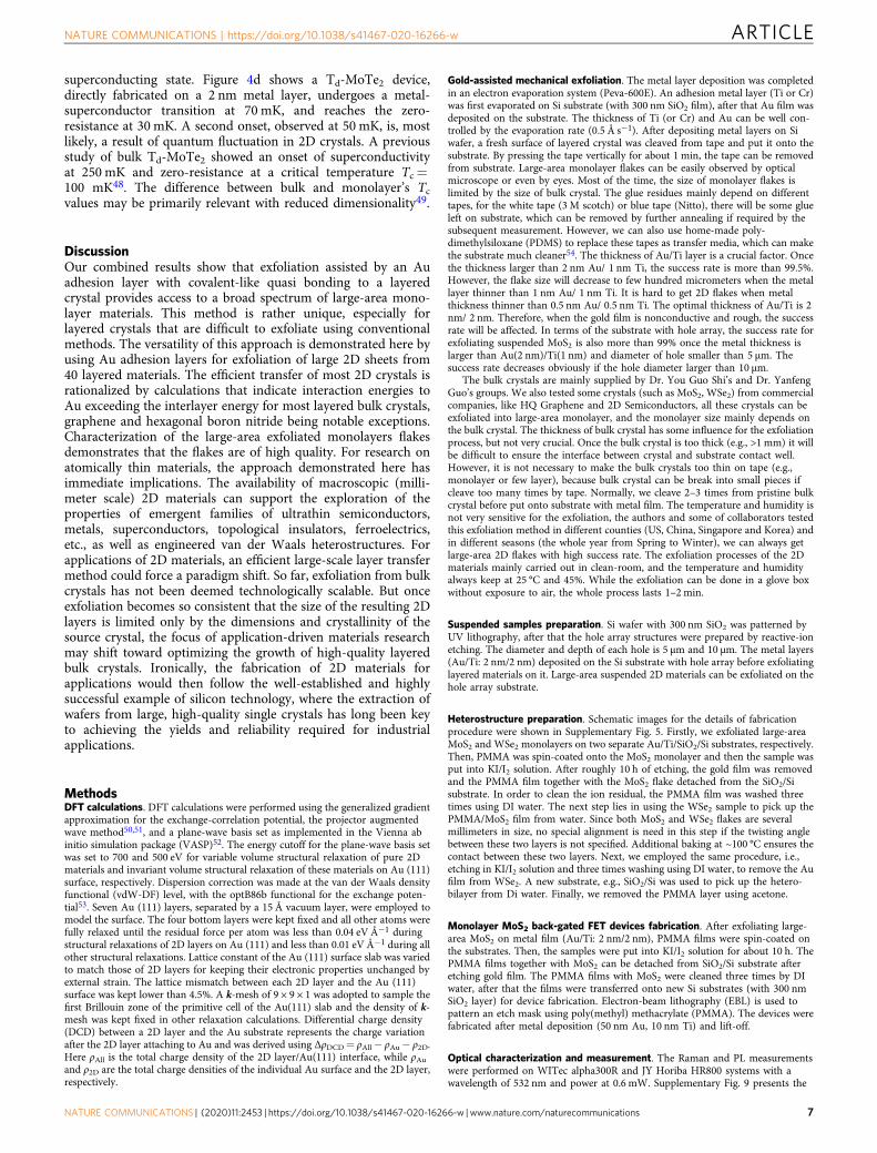
Surface characterization of as-exfoliated samples. High-qualitymacroscopic monolayers have practical advantages, for instancein establishing the lattice structure and electronic band structureof unexplored 2D materials or van der Waals stacks by scanningtunneling microscopy (STM) and ARPES. The Au-coated supportfacilitates such electron-based spectroscopy by eliminating char-ging effects associated with insulating (e.g., SiO2) substrates whilepreserving the intrinsic electronic band structures. Figure 3a, billustrates atomic-resolution STM images for as-exfoliated WSe2and Td-MoTe2 monolayers, which are challenging to image oninsulating substrates due to charging effects. Low-energy electrondiffraction with millimeter incident electron-beam size shows asingle-phase diffraction pattern for MoTe2 (Fig. 3c), indicatingthat it is a single-crystal at the millimeter scale. Figure 3d displaysan ARPES map of the low-energy electronic structure of the WSe2monolayer, showing clear and sharp bands. The valence bandfeatures a single flat band around Γ and a large band splitting nearK. Along the Γ-K line, one single band starts to split into twospin-resolved bands at k � 1
3ΔkK;Γ, and the valence band max-
imum at K sits at ~0.6 eV higher than that at Γ. Figure 3e displaysthe symmetric band splitting spectra along K–M–K’ arising fromstrong spin-orbit coupling mainly at the W site in the WSe2lattice39. These features constitute the critical signatures of banddispersion in monolayer TMDCs. Here it deserves an emphasison the big advantage of large area of monolayer TMDCs, whichmake it quite feasible and easy to accurately measure the bandstructure by using standard ARPES technique40.
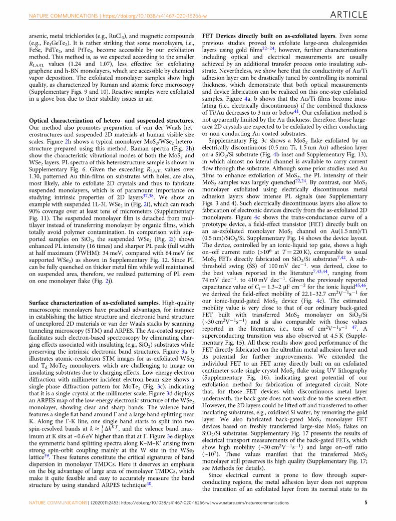
FET Devices directly built on as-exfoliated layers. Even someprevious studies proved to exfoliate large-area chalcogenideslayers using gold films22–24; however, further characterizationsincluding optical and electrical measurements are usuallyachieved by an additional transfer process onto insulating sub-strate. Nevertheless, we show here that the conductivity of Au/Tiadhesion layer can be drastically tuned by controlling its nominalthickness, which demonstrate that both optical measurementsand device fabrication can be realized on this one-step exfoliatedsamples. Figure 4a, b shows that the Au/Ti films become insu-lating (i.e., electrically discontinuous) if the combined thicknessof Ti/Au decreases to 3 nm or below41. Our exfoliation method isnot apparently limited by the Au thickness, therefore, those large-area 2D crystals are expected to be exfoliated by either conductingor non-conducting Au-coated substrates.
Supplementary Fig. 3c shows a MoS2 flake exfoliated by anelectrically discontinuous (0.5 nm Ti, 1.5 nm Au) adhesion layeron a SiO2/Si substrate (Fig. 4b inset and Supplementary Fig. 13),in which almost no lateral channel is available to carry currentflow through the substrate. Although some prior studies used Aufilms to enhance exfoliation of MoS2, the PL intensity of theirMoS2 samples was largely quenched22,24. By contrast, our MoS2monolayer exfoliated using electrically discontinuous metaladhesion layers show intense PL signals (see SupplementaryFigs. 3 and 4). Such electrically discontinuous layers also allow tofabrication of electronic devices directly from the as-exfoliated 2Dmonolayers. Figure 4c shows the trans-conductance curve of aprototype device, a field-effect transistor (FET) directly built onan as-exfoliated monolayer MoS2 channel on Au(1.5 nm)/Ti(0.5 nm)/SiO2/Si. Supplementary Fig. 14 shows the device layout.The device, controlled by an ionic-liquid top gate, shows a highon–off current ratio (>106 at T= 220 K), comparable to usualMoS2 FETs directly fabricated on SiO2/Si substrates7,42. A sub-threshold swing (SS) of 100 mV dec−1. was derived, close tothe best values reported in the literature7,43,44, ranging from74mV dec−1. to 410 mV dec−1. Given the previously reportedcapacitance value of Ci= 1.3~2 μF cm−2 for the ionic liquid45,46,we derived the field-effect mobility of 22.1–32.7 cm2V−1s−1 forour ionic-liquid-gated MoS2 device (Fig. 4c). The estimatedmobility value is very close to that of our ordinary back-gatedFET built with transferred MoS2 monolayer on SiO2/Si(~30 cm2V−1s−1) and is also comparable with those valuesreported in the literature, i.e., tens of cm2V−1s−1 47. Asuperconducting transition was also observed at 4.5 K (Supple-mentary Fig. 15). All these results show good performance of theFET directly fabricated on the ultrathin metal adhesion layer andits potential for further improvements. We extended theindividual FET to an FET array directly built on an exfoliatedcentimeter-scale single-crystal MoS2 flake using UV lithography(Supplementary Fig. 16), indicating great potential of ourexfoliation method for fabrication of integrated circuit. Notethat, for those FET devices with discontinuous metal layerunderneath, the back gate does not work due to the screen effect.However, the 2D layers could be lifted off and transferred to otherinsulating substrates, e.g., oxidized Si wafer, by removing the goldlayer. We also fabricated back-gated MoS2 monolayer FETdevices based on freshly transferred large-size MoS2 flakes onSiO2/Si substrates. Supplementary Fig. 17 presents the results ofelectrical transport measurements of the back-gated FETs, whichshow high mobility (~30 cm2V−1s−1) and large on–off ratio(~107). These values manifest that the transferred MoS2monolayer still preserves its high quality (Supplementary Fig. 17;see Methods for details).
Since electrical current is prone to flow through super-conducting regions, the metal adhesion layer does not suppressthe transition of an exfoliated layer from its normal state to its
NATURE COMMUNICATIONS | https://doi.org/10.1038/s41467-020-16266-w ARTICLE
NATURE COMMUNICATIONS | (2020) 11:2453 | https://doi.org/10.1038/s41467-020-16266-w |www.nature.com/naturecommunications 5

ba
b
1 nm
e K M K’a
0.5 nm
a
b
WSe2
MoTe2
d Γ
K//(1/Å) K//(1/Å)
c
a
b
K
1L WSe2 1L WSe2
0
–1
0
–1
–2
–3–2
0 1 –0.5
High High
Low Low
0.5E
– E
F (
eV)
E –
EF (
eV)
MoTe2
Fig. 3 STM and ARPES measurements of 2D materials exfoliated onto conductive Au/Ti adhesion layers. a, b STM images of monolayer WSe2 and Td-MoTe2, respectively. c LEED pattern of monolayer Td-MoTe2. d, e Band structure of monolayer WSe2. d Original ARPES band structure of monolayer WSe2(hv= 21.2 eV) along Γ-K high symmetry line. The valence band maximum (VBM) is positioned at K instead of Γ, which is an important signature ofmonolayer WSe2. e Second-derivative spectra of band dispersion along K–M–K’, showing clear spin-orbital coupling (SOC) induced spin-splitting bands.
1E–12
1E–11
1E–10
1E–9
1E–8
1E–7
1E–6
1E–5
1E–4
1E–3
0.01
0.1C
urre
nt (
A)
Metal layer thickness
b
Au/Ti:2 nm/2 nm
Au:1 nm 50°
–50°
0.0 phase 1 μm0.0 phase 1 μm
Vsd = 0.4 V
Au1 nm
Au/Ti: 1.5 nm/0.5 nm
Vg = –0.5 to 0.6 VStep: 0.1 V
MoS2
Vsd = 0.1V
Gate voltage (V)
Con
duct
ance
� (S
)
–2 –1 0 1 2 3 41E–11
1E–10
1E–9
1E–8
1E–7
1E–6
1E–5
1E–4
–0.4 –0.2 0.0 0.2 0.4
–3 μ
–2 μ
–1 μ
0
1 μ
2 μ
3 μ
I sd (u
A)
Vsd (V)
c
0.0 0.2 0.4 0.6 0.8 1.0 1.2 1.4 1.6 1.8 2.0
0
5
10
15
20
25
30
Rxx
(Ω
)
T (K)
Iac = 10 nA0.00 0.02 0.04 0.06 0.08 0.10
0
5
10
15
20
25
30
Rxx
[Ω]
T [K]
d
Td-MoTe2 Au/Ti: 1.5 nm/0.5 nm
Au/Ti: 2 nm/2 nm
0.0
6.0 × 10⁻³
4.0 × 10⁻³
2.0 × 10⁻³
–2.0 × 10⁻³
–4.0 × 10⁻³
–6.0 × 10⁻³
–0.5 –0.4 –0.3 –0.2 –0.1 0.0 0.1 0.2 0.3 0.4 0.5
0.0
5.0×10⁻¹³
–5.0 × 10⁻¹³
–1.0 × 10⁻¹²
–1.5 × 10⁻¹²
–2.0 × 10⁻¹²
–2.5 × 10⁻¹²
–3.0 × 10⁻¹²
Cur
rent
(A
)
Voltage (V)
aAu/Ti: 1 nm/2 nm
Au/Ti2 nm/2 nm
Au/Ti3 nm/2 nm
Au/Ti1 nm/1 nm Au/Ti
1 nm/2 nm
Au/Ti1 nm/2 nm
Fig. 4 Electrical measurements of metal adhesion layers and of 2D materials exfoliated onto nonconductive metal films. a Electrical transfer curves oftypical Au/Ti adhesion layers. b Two-terminal resistance of Au/Ti layers with different nominal thickness. The inset shows atomic force microscope (AFM)phase maps of two metal layers. c Gate voltage-conductance transfer characteristics of a top-gated MoS2 FET on SiO2/Si with Au (1.5 nm)/Ti (0.5 nm)adhesion layer (T= 220 K, source−drain bias Vsd= 0.1 V). Left inset: Optical image of the FET device with windows for the ionic-liquid top gate. Rightinset: low-bias source-drain current-voltage characteristics for gate voltage −0.5 to 0.6 V. d Temperature-dependent resistance of a Td-MoTe2 flakeexfoliated onto SiO2/Si with a 2 nm metal adhesion layer.
ARTICLE NATURE COMMUNICATIONS | https://doi.org/10.1038/s41467-020-16266-w
6 NATURE COMMUNICATIONS | (2020) 11:2453 | https://doi.org/10.1038/s41467-020-16266-w |www.nature.com/naturecommunications
superconducting state. Figure 4d shows a Td-MoTe2 device,directly fabricated on a 2 nm metal layer, undergoes a metal-superconductor transition at 70 mK, and reaches the zero-resistance at 30 mK. A second onset, observed at 50 mK, is, mostlikely, a result of quantum fluctuation in 2D crystals. A previousstudy of bulk Td-MoTe2 showed an onset of superconductivityat 250 mK and zero-resistance at a critical temperature Tc=100 mK48. The difference between bulk and monolayer’s Tcvalues may be primarily relevant with reduced dimensionality49.
DiscussionOur combined results show that exfoliation assisted by an Auadhesion layer with covalent-like quasi bonding to a layeredcrystal provides access to a broad spectrum of large-area mono-layer materials. This method is rather unique, especially forlayered crystals that are difficult to exfoliate using conventionalmethods. The versatility of this approach is demonstrated here byusing Au adhesion layers for exfoliation of large 2D sheets from40 layered materials. The efficient transfer of most 2D crystals isrationalized by calculations that indicate interaction energies toAu exceeding the interlayer energy for most layered bulk crystals,graphene and hexagonal boron nitride being notable exceptions.Characterization of the large-area exfoliated monolayers flakesdemonstrates that the flakes are of high quality. For research onatomically thin materials, the approach demonstrated here hasimmediate implications. The availability of macroscopic (milli-meter scale) 2D materials can support the exploration of theproperties of emergent families of ultrathin semiconductors,metals, superconductors, topological insulators, ferroelectrics,etc., as well as engineered van der Waals heterostructures. Forapplications of 2D materials, an efficient large-scale layer transfermethod could force a paradigm shift. So far, exfoliation from bulkcrystals has not been deemed technologically scalable. But onceexfoliation becomes so consistent that the size of the resulting 2Dlayers is limited only by the dimensions and crystallinity of thesource crystal, the focus of application-driven materials researchmay shift toward optimizing the growth of high-quality layeredbulk crystals. Ironically, the fabrication of 2D materials forapplications would then follow the well-established and highlysuccessful example of silicon technology, where the extraction ofwafers from large, high-quality single crystals has long been keyto achieving the yields and reliability required for industrialapplications.
MethodsDFT calculations. DFT calculations were performed using the generalized gradientapproximation for the exchange-correlation potential, the projector augmentedwave method50,51, and a plane-wave basis set as implemented in the Vienna abinitio simulation package (VASP)52. The energy cutoff for the plane-wave basis setwas set to 700 and 500 eV for variable volume structural relaxation of pure 2Dmaterials and invariant volume structural relaxation of these materials on Au (111)surface, respectively. Dispersion correction was made at the van der Waals densityfunctional (vdW-DF) level, with the optB86b functional for the exchange poten-tial53. Seven Au (111) layers, separated by a 15 Å vacuum layer, were employed tomodel the surface. The four bottom layers were kept fixed and all other atoms werefully relaxed until the residual force per atom was less than 0.04 eV Å−1 duringstructural relaxations of 2D layers on Au (111) and less than 0.01 eV Å−1 during allother structural relaxations. Lattice constant of the Au (111) surface slab was variedto match those of 2D layers for keeping their electronic properties unchanged byexternal strain. The lattice mismatch between each 2D layer and the Au (111)surface was kept lower than 4.5%. A k-mesh of 9 × 9 × 1 was adopted to sample thefirst Brillouin zone of the primitive cell of the Au(111) slab and the density of k-mesh was kept fixed in other relaxation calculations. Differential charge density(DCD) between a 2D layer and the Au substrate represents the charge variationafter the 2D layer attaching to Au and was derived using ΔρDCD= ρAll− ρAu− ρ2D.Here ρAll is the total charge density of the 2D layer/Au(111) interface, while ρAuand ρ2D are the total charge densities of the individual Au surface and the 2D layer,respectively.
Gold-assisted mechanical exfoliation. The metal layer deposition was completedin an electron evaporation system (Peva-600E). An adhesion metal layer (Ti or Cr)was first evaporated on Si substrate (with 300 nm SiO2 film), after that Au film wasdeposited on the substrate. The thickness of Ti (or Cr) and Au can be well con-trolled by the evaporation rate (0.5 Å s−1). After depositing metal layers on Siwafer, a fresh surface of layered crystal was cleaved from tape and put it onto thesubstrate. By pressing the tape vertically for about 1 min, the tape can be removedfrom substrate. Large-area monolayer flakes can be easily observed by opticalmicroscope or even by eyes. Most of the time, the size of monolayer flakes islimited by the size of bulk crystal. The glue residues mainly depend on differenttapes, for the white tape (3 M scotch) or blue tape (Nitto), there will be some glueleft on substrate, which can be removed by further annealing if required by thesubsequent measurement. However, we can also use home-made poly-dimethylsiloxane (PDMS) to replace these tapes as transfer media, which can makethe substrate much cleaner54. The thickness of Au/Ti layer is a crucial factor. Oncethe thickness larger than 2 nm Au/ 1 nm Ti, the success rate is more than 99.5%.However, the flake size will decrease to few hundred micrometers when the metallayer thinner than 1 nm Au/ 1 nm Ti. It is hard to get 2D flakes when metalthickness thinner than 0.5 nm Au/ 0.5 nm Ti. The optimal thickness of Au/Ti is 2nm/ 2 nm. Therefore, when the gold film is nonconductive and rough, the successrate will be affected. In terms of the substrate with hole array, the success rate forexfoliating suspended MoS2 is also more than 99% once the metal thickness islarger than Au(2 nm)/Ti(1 nm) and diameter of hole smaller than 5 μm. Thesuccess rate decreases obviously if the hole diameter larger than 10 μm.
The bulk crystals are mainly supplied by Dr. You Guo Shi’s and Dr. YanfengGuo’s groups. We also tested some crystals (such as MoS2, WSe2) from commercialcompanies, like HQ Graphene and 2D Semiconductors, all these crystals can beexfoliated into large-area monolayer, and the monolayer size mainly depends onthe bulk crystal. The thickness of bulk crystal has some influence for the exfoliationprocess, but not very crucial. Once the bulk crystal is too thick (e.g., >1 mm) it willbe difficult to ensure the interface between crystal and substrate contact well.However, it is not necessary to make the bulk crystals too thin on tape (e.g.,monolayer or few layer), because bulk crystal can be break into small pieces ifcleave too many times by tape. Normally, we cleave 2–3 times from pristine bulkcrystal before put onto substrate with metal film. The temperature and humidity isnot very sensitive for the exfoliation, the authors and some of collaborators testedthis exfoliation method in different counties (US, China, Singapore and Korea) andin different seasons (the whole year from Spring to Winter), we can always getlarge-area 2D flakes with high success rate. The exfoliation processes of the 2Dmaterials mainly carried out in clean-room, and the temperature and humidityalways keep at 25 °C and 45%. While the exfoliation can be done in a glove boxwithout exposure to air, the whole process lasts 1–2 min.
Suspended samples preparation. Si wafer with 300 nm SiO2 was patterned byUV lithography, after that the hole array structures were prepared by reactive-ionetching. The diameter and depth of each hole is 5 μm and 10 μm. The metal layers(Au/Ti: 2 nm/2 nm) deposited on the Si substrate with hole array before exfoliatinglayered materials on it. Large-area suspended 2D materials can be exfoliated on thehole array substrate.
Heterostructure preparation. Schematic images for the details of fabricationprocedure were shown in Supplementary Fig. 5. Firstly, we exfoliated large-areaMoS2 and WSe2 monolayers on two separate Au/Ti/SiO2/Si substrates, respectively.Then, PMMA was spin-coated onto the MoS2 monolayer and then the sample wasput into KI/I2 solution. After roughly 10 h of etching, the gold film was removedand the PMMA film together with the MoS2 flake detached from the SiO2/Sisubstrate. In order to clean the ion residual, the PMMA film was washed threetimes using DI water. The next step lies in using the WSe2 sample to pick up thePMMA/MoS2 film from water. Since both MoS2 and WSe2 flakes are severalmillimeters in size, no special alignment is need in this step if the twisting anglebetween these two layers is not specified. Additional baking at ~100 °C ensures thecontact between these two layers. Next, we employed the same procedure, i.e.,etching in KI/I2 solution and three times washing using DI water, to remove the Aufilm from WSe2. A new substrate, e.g., SiO2/Si was used to pick up the hetero-bilayer from Di water. Finally, we removed the PMMA layer using acetone.
Monolayer MoS2 back-gated FET devices fabrication. After exfoliating large-area MoS2 on metal film (Au/Ti: 2 nm/2 nm), PMMA films were spin-coated onthe substrates. Then, the samples were put into KI/I2 solution for about 10 h. ThePMMA films together with MoS2 can be detached from SiO2/Si substrate afteretching gold film. The PMMA films with MoS2 were cleaned three times by DIwater, after that the films were transferred onto new Si substrates (with 300 nmSiO2 layer) for device fabrication. Electron-beam lithography (EBL) is used topattern an etch mask using poly(methyl) methacrylate (PMMA). The devices werefabricated after metal deposition (50 nm Au, 10 nm Ti) and lift-off.
Optical characterization and measurement. The Raman and PL measurementswere performed on WITec alpha300R and JY Horiba HR800 systems with awavelength of 532 nm and power at 0.6 mW. Supplementary Fig. 9 presents the
NATURE COMMUNICATIONS | https://doi.org/10.1038/s41467-020-16266-w ARTICLE
NATURE COMMUNICATIONS | (2020) 11:2453 | https://doi.org/10.1038/s41467-020-16266-w |www.nature.com/naturecommunications 7

representative Raman spectra for monolayer and few-layer BP and α-RuCl3 sam-ples excited by 2.33 eV radiation in vacuum environments. The laser power on thesample during Raman measurement was kept below 100 μW in order to avoidsample damage and excessive heating. The silicon Raman mode at 520.7 cm−1 wasused for calibration prior to measurements and as an internal frequency reference.
X-ray photoelectron spectroscopy characterization. The X-ray photoelectronspectroscopy (XPS, Thermo Scientific ESCALAB 250 Xi) was performed with AlKα X-rays (hυ= 1486.6 eV) in an analysis chamber that had a base pressure < 3 ×10⁻⁹ Torr. Core spectra were recorded using a 50 eV constant pass energy (PE) in50–100 μm small area lens mode (i.e., aperture selected area). The XPS peaks werecalibrated using the adventitious carbon C1s peak position (284.8 eV).
Scanning probe microscopy measurements. The AFM scanning (Veeco Multi-mode III) was used to check the thickness and surface morphology of thosemonolayer samples. The STM measurement was performed using a custom built,low-temperature, and UHV STM system at 300 K. A chemically etched W STM tipwas cleaned and calibrated against a gold (111) single crystal prior to the mea-surements. For STM and ARPES measurements, the 2D layers were exfoliated ontoan Au(5 nm)/Ti(2 nm)/SiO2(~300 nm)/Si substrate. An annealing process at 500 Kfor 2 h was performed to degas the samples after loading them into the high-vacuum chamber.
Angle-resolved photoemission spectroscopy measurement. High resolutionARPES measurements were carried out on our lab system equipped with a ScientaR4000 electron energy analyzer55. We use Helium discharge lamp as the lightsource, which can provide photon energies of hυ= 21.218 eV (Helium I). Theenergy resolution was set at 10–20 meV for band structure measurements (Fig. 3).The angular resolution is ~0.3 degree. The Fermi level is referenced by measuringon a clean polycrystalline gold that is electrically connected to the sample. Thesamples were measured in vacuum with a base pressure better than 5 × 10⁻¹¹ Torr.The ARPES measurements for WSe2 and MoS2 monolayers were carried out atroughly 30 K using a home-build photoemission spectroscopy system with aVUV5000 Helium lamp. The spot diameter of the Helium lamp is 0.5 mm.
FET characterization and measurement. The electrical characteristic measure-ments were carried out in the probe station with the semiconductor parameteranalyzers (Agilent 4156 C and B1500) and oscilloscope. The ionic liquid used fortop-gated MoS2 FET device is N-diethyl-N-(2-methoxyethyl)-N-methylammo-nium bis-(trifuoromethylsulfonyl)-imide (DEME–TFSI), which has been widelyused in 2D-material-based devices.
Online content. Methods, along with any Supplementary Information displayitems and Source Data, are available in the online version of the paper; referencesunique to these sections appear only in the online paper.
Data availabilityAll data needed to evaluate the conclusions in the paper are present in the paper and/orthe Supplementary Information. Additional data related to this paper may be requestedfrom the authors.
Received: 11 February 2020; Accepted: 21 April 2020;
References1. He, S. L. et al. Phase diagram and electronic indication of high-temperature
superconductivity at 65 K in single-layer FeSe films. Nat. Mater. 12, 605–610(2013).
2. Zhang, C. et al. Engineering point-defect states in monolayer WSe2. ACS Nano13, 1595–1602 (2019).
3. Ezawa, M. Valley-polarized metals and quantum anomalous hall effect insilicene. Phys. Rev. Lett. 109, 055502 (2012).
4. Jiang, S. W., Li, L. Z., Wang, Z. F., Mak, K. F. & Shan, J. Controllingmagnetism in 2D CrI3 by electrostatic doping. Nat. Nanotechnol. 13, 549–553(2018).
5. Novoselov, K. S. et al. Electric field effect in atomically thin carbon films.Science 306, 666–669 (2004).
6. Huang, Y. et al. Reliable exfoliation of large-area high-quality flakes ofgraphene and other two-dimensional materials. ACS Nano 9, 10612–10620(2015).
7. Radisavljevic, B., Radenovic, A., Brivio, J., Giacometti, V. & Kis, A. Single-layerMoS2 transistors. Nat. Nanotechnol. 6, 147–150 (2011).
8. McGuire, M. A., Dixit, H., Cooper, V. R. & Sales, B. C. Coupling of crystalstructure and magnetism in the layered, ferromagnetic insulator CrI3. Chem.Mater. 27, 612–620 (2015).
9. Jiang, D. et al. High-Tc superconductivity in ultrathin Bi2Sr2CaCu2O8+x downto half-unit-cell thickness by protection with graphene. Nat. Commun. 5, 5708(2014).
10. Tang, S. J. et al. Quantum spin Hall state in monolayer 1T’-WTe2. Nat. Phys.13, 683–687 (2017).
11. Zhang, Y. et al. Superconducting gap anisotropy in monolayer FeSe thin film.Phys. Rev. Lett. 117, 117001 (2016).
12. Novoselov, K. S., Mishchenko, A., Carvalho, A. & Neto, A. H. C. 2D materialsand van der Waals heterostructures. Science 353, 9439 (2016).
13. Liu, Y. et al. Van der Waals heterostructures and devices. Nat. Rev. Mater. 1,16042 (2016).
14. Wang, C. et al. Monolayer atomic crystal molecular superlattices. Nature 555,231–236 (2018).
15. Li, X. S., Cai, W. W., Colombo, L. & Ruoff, R. S. Evolution of graphene growthon Ni and Cu by carbon isotope labeling. Nano Lett. 9, 4268–4272 (2009).
16. Moon, I. K., Lee, J., Ruoff, R. S. & Lee, H. Reduced graphene oxide by chemicalgraphitization. Nat. Commun. 1, 73 (2010).
17. Sutter, P. W., Flege, J. I. & Sutter, E. A. Epitaxial graphene on ruthenium. Nat.Mater. 7, 406–411 (2008).
18. Meng, L. et al. Buckled silicene formation on Ir(111). Nano Lett. 13, 685–690(2013).
19. Liu, H., Du, Y. C., Deng, Y. X. & Ye, P. D. Semiconducting black phosphorus:synthesis, transport properties and electronic applications. Chem. Soc. Rev. 44,2732–2743 (2015).
20. Coleman, J. N. et al. Two-dimensional nanosheets produced by liquidexfoliation of layered. Mater. Sci. 331, 568–571 (2011).
21. Fan, X. B. et al. Fast and efficient preparation of exfoliated 2H MoS2nanosheets by sonication-assisted lithium intercalation and infrared laser-induced 1T to 2H phase reversion. Nano Lett. 15, 5956–5960 (2015).
22. Desai, S. B. et al. Gold-mediated exfoliation of ultralarge optoelectronically-perfect monolayers. Adv. Mater. 28, 4053–4058 (2016).
23. Velicky, M. et al. Mechanism of gold-assisted exfoliation of centimeter-sizedtransition-metal dichalcogenide monolayers. ACS Nano 12, 10463–10472(2018).
24. Magda, G. Z. et al. Exfoliation of large-area transition metal chalcogenidesingle layers. Sci. Rep. 5, 14714 (2015).
25. Zhang, Y. B., Tan, Y. W., Stormer, H. L. & Kim, P. Experimental observationof the quantum Hall effect and Berry’s phase in graphene. Nature 438,201–204 (2005).
26. Novoselov, K. S. et al. Two-dimensional gas of massless Dirac fermions ingraphene. Nature 438, 197–200 (2005).
27. Cao, Y. et al. Unconventional superconductivity in magic-angle graphenesuperlattices. Nature 556, 43–50 (2018).
28. Hao, Y. F. et al. Oxygen-activated growth and bandgap tunability of largesingle-crystal bilayer graphene. Nat. Nanotechnol. 11, 426–431 (2016).
29. Qiao, J. S., Kong, X. H., Hu, Z. X., Yang, F. & Ji, W. High-mobility transportanisotropy and linear dichroism in few-layer black phosphorus. Nat.Commun. 5, 4475 (2014).
30. Hu, Z.-X., Kong, X., Qiao, J., Normand, B. & Ji, W. Interlayer electronichybridization leads to exceptional thickness-dependent vibrational propertiesin few-layer black phosphorus. Nanoscale 8, 2740–2750 (2016).
31. Qiao, J. et al. Few-layer Tellurium: one-dimensional-like layered elementarysemiconductor with striking physical properties. Sci. Bull. 63, 159–168(2018).
32. Li, W. et al. Experimental realization of honeycomb borophene. Sci. Bull. 63,282–286 (2018).
33. Deng, Y. et al. Gate-tunable room-temperature ferromagnetism in two-dimensional Fe3GeTe2. Nature 563, 94–99 (2018).
34. Giovannetti, G. et al. Doping graphene with metal contacts. Phys. Rev. Lett.101, 026803 (2008).
35. Li, H. et al. From bulk to monolayer MoS2: evolution of Raman scattering.Adv. Funct. Mater. 22, 1385–1390 (2012).
36. Mak, K. F., Lee, C., Hone, J., Shan, J. & Heinz, T. F. Atomically thin MoS2: anew Direct-gap semiconductor. Phys. Rev. Lett. 105, 136805 (2010).
37. Du, X., Skachko, I., Barker, A. & Andrei, E. Y. Approaching ballistic transportin suspended graphene. Nat. Nanotechnol. 3, 491–495 (2008).
38. Lee, C., Wei, X. D., Kysar, J. W. & Hone, J. Measurement of the elasticproperties and intrinsic strength of monolayer graphene. Science 321, 385–388(2008).
39. Zhang, Y. et al. Electronic structure, surface doping, and optical response inepitaxial WSe2 thin films. Nano Lett. 16, 2485–2491 (2016).
40. Zhang, H. Y. et al. Resolving deep quantum-well states in atomically thin 2H-MoTe2 flakes by nanospot angle-resolved photoemission spectroscopy. NanoLett. 18, 4664–4668 (2018).
ARTICLE NATURE COMMUNICATIONS | https://doi.org/10.1038/s41467-020-16266-w
8 NATURE COMMUNICATIONS | (2020) 11:2453 | https://doi.org/10.1038/s41467-020-16266-w |www.nature.com/naturecommunications

41. Frydendahl, C. et al. Optical reconfiguration and polarization control in semi-continuous gold films close to the percolation threshold. Nanoscale 9,12014–12024 (2017).
42. Yoon, Y., Ganapathi, K. & Salahuddin, S. How good can monolayer MoS2transistors be? Nano Lett. 11, 3768–3773 (2011).
43. Liu, W., Sarkar, D., Kang, J. H., Cao, W. & Banerjee, K. Impact of contact onthe operation and performance of back-gated monolayer MoS2 field-effect-transistors. ACS Nano 9, 7904–7912 (2015).
44. Kappera, R. et al. Phase-engineered low-resistance contacts for ultrathin MoS2transistors. Nat. Mater. 13, 1128–1134 (2014).
45. Zhan, C., Neal, J., Wu, J. & Jiang, D. E. Quantum effects on the capacitance ofgraphene-based electrodes. J. Phys. Chem. C. 119, 22297–22303 (2015).
46. Fujimoto, T. & Awaga, K. Electric-double-layer field-effect transistors withionic liquids. Phys. Chem. Chem. Phys. 15, 8983–9006 (2013).
47. Ganatra, R. & Zhang, Q. Few-Layer MoS2: a promising layered semiconductor.ACS Nano 8, 4074–4099 (2014).
48. Qi, Y. P. et al. Superconductivity in Weyl semimetal candidate MoTe2. Nat.Commun. 7, 11038 (2016).
49. Xi, X. et al. Ising pairing in superconducting NbSe2 atomic layers. Nat. Phys.12, 139–143 (2016).
50. Blöchl, P. E. Projector augmented-wave method. Phys. Rev. B 50, 17953–17979(1994).
51. Kresse, G. & Joubert, D. From ultrasoft pseudopotentials to the projectoraugmented-wave method. Phys. Rev. B 59, 1758–1775 (1999).
52. Kresse, G. & Furthmüller, J. Efficient iterative schemes for ab initio total-energy calculations using a plane-wave basis set. Phys. Rev. B 54, 11169–11186(1996).
53. Klimes, J., Bowler, D. R. & Michaelides, A. Van der Waals density functionalsapplied to solids. Phys. Rev. B 83, 195131 (2011).
54. Jain, A. et al. Minimizing residues and strain in 2D materials transferred fromPDMS. Nanotechnology 29, 265203 (2018).
55. Liu, G. D. et al. Development of a vacuum ultraviolet laser-based angle-resolved photoemission system with a superhigh energy resolution better than1 meV. Rev. Sci. Instrum. 79, 023105 (2008).
AcknowledgementsWe would like to thank Dr. Zhongming Wei, Xianjue Chen and Jia Wang for valuablediscussions about XPS. This work is supported by the National Key Research andDevelopment Program of China (Grant No. 2019YFA0308000, 2018YFA0305800,2018YFE0202700, 2018YFA0704201), the Youth Innovation Promotion Association ofCAS (2019007, 2018013, 2017013), the National Natural Science Foundation of China(Grant No. 11874405, 11622437, 61674171, 61725107, 61971035, and 11974422), theNational Basic Research Program of China (Grant No. 2015CB921300), and the StrategicPriority Research Program (B) of the Chinese Academy of Sciences (Grant No.XDB25000000, XDB30000000), the Research Program of Beijing Academy of QuantumInformation Sciences (Grant No. Y18G06). P.S. and E.S. acknowledge support by the U.S.Department of Energy, Office of Science, Basic Energy Sciences, under Award No. DE-SC0016343. Calculations were performed at the Physics Lab of High-PerformanceComputing of Renmin University of China and Shanghai Supercomputer Center.
Author contributionsP.S., W.J., H.J.G., and X.J.Z. are equally responsible for supervising the discovery. Y.H.and R.Y. conceived the project. Y.H.P., J.P.H., and J.W. performed the DFT calculations.Y.H., H.L.L., and L.L. prepared all the mechanical exfoliation samples. Y.H. and R.Y.performed the Raman, PL and AFM measurements. M.H., J.W., P.S., and E.S. performedXPS measurement. Y.Q.C., G.D.L., L.Z., and W.J.Z. performed the ARPES measurement.Z.L.Z., P.C., K.H.W., L.M., Z.Z., L.W.L, and Y.L.W performed the STM and LEEDmeasurement. Y.G.S. and Y.F.G. prepared bulk layered crystals. S.B.T., C.Z.G., Z.G.C., L.M.W. G.H.Y., and L.H.B. fabricated the transistors and performed the electrical mea-surements. Y.H., Y.H.P., R.Y., J.P.H., P.S., and W.J. analyzed data, wrote the manuscriptand all authors discussed and commented on it.
Competing interestsThe authors declare the following competing interests that three Chinese patents werefiled (201910529797.7; 201910529796.2; 201910529623.0) by the Institute of Physics,Chinese Academy of Sciences, along with their researchers (Y.H., H.L.L., and X.J.Z).
Additional informationSupplementary information is available for this paper at https://doi.org/10.1038/s41467-020-16266-w.
Correspondence and requests for materials should be addressed to P.S., W.J., X.-J.Z. orH.-J.G.
Peer review information Nature Communications thanks Peter Bøggild, Kai-Qiang Lin,and the other, anonymous, reviewer(s) for their contribution to the peer review of thiswork. Peer review reports are available.
Reprints and permission information is available at http://www.nature.com/reprints
Publisher’s note Springer Nature remains neutral with regard to jurisdictional claims inpublished maps and institutional affiliations.
Open Access This article is licensed under a Creative CommonsAttribution 4.0 International License, which permits use, sharing,
adaptation, distribution and reproduction in any medium or format, as long as you giveappropriate credit to the original author(s) and the source, provide a link to the CreativeCommons license, and indicate if changes were made. The images or other third partymaterial in this article are included in the article’s Creative Commons license, unlessindicated otherwise in a credit line to the material. If material is not included in thearticle’s Creative Commons license and your intended use is not permitted by statutoryregulation or exceeds the permitted use, you will need to obtain permission directly fromthe copyright holder. To view a copy of this license, visit http://creativecommons.org/licenses/by/4.0/.
© The Author(s) 2020
NATURE COMMUNICATIONS | https://doi.org/10.1038/s41467-020-16266-w ARTICLE
NATURE COMMUNICATIONS | (2020) 11:2453 | https://doi.org/10.1038/s41467-020-16266-w |www.nature.com/naturecommunications 9