memorias del 1er taller de atomic layer deposition...
TRANSCRIPT

Memorias del 1er Taller de Atomic Layer Deposition ALD Depósito de Capas Atómicas El 7 y 8 de Mayo se llevó acabo el 1er taller de depósito de capas atómicas en las instalaciones de ciudad universitaria de la UACJ. Es estas memorias se encuentran los trabajos expuestos por parte de investigadores y estudiantes.
2015
Universidad Autónoma de Ciudad Juárez
5/7/2015

2
Directorio
Universidad Autónoma de Ciudad Juárez
Lic. Ricardo Duarte Jáquez Rector
Instituto de Ingeniería y Tecnología Maestro Francisco López Hernández
Departamento de Física y Matemáticas Maestro Natividad Nieto Saldaña
División Multidisciplinaria Ciudad Universitaria
Maestro Absalón Uruchurtu Moreno
3
Comité
Mtro. Absalón Uruchurtu Moreno
Mtro. Rene Noriega Armendáriz
Mtro. Manuel Alberto Rodríguez Esparza
Mtra. Mónica Padilla García
Física de Materiales: CAFiM (UACJ-CA-80)
Dra. Diana María Carrillo Flores
Dr. Juan Francisco Hernández Paz
Dr. José Trinidad Elizalde Galindo
Dr. Manuel Antonio Ramos Murillo
Dr. José Rurik Farías Mancilla
Dr. José Luis Enríquez Carrejo
Dr. Pierre Giovanni Maní González

4
Índice 1er Taller ALD
1. Ponencias ALD………………………………………………………………………………..5
2. Posters ALD…………………………………………………………………………………...6
3. A detailed assessment of indium diffusion in ALD-grown
high-k dielectrics employing ARXPS……………………………………………………….7
4. Propiedades magnéticas con primeros principios
utilizando DFT................................................................................................................8
5. A flexible solar cell using atomic layer deposition………………………………………...9
6. Growth conditions and crystallographic properties of zno nanorod arrays using
ald……………………………………………………………………………………………...10
7. Vertically aligned ZnO nanorods growth using textured ZnO films
produced by ALD……………………………………………………………………………..11
8. Growth of ZnO ultrathin films by atomic layer deposition .............................................12
9. Electrical properties of zno/al2o3 nanocomposites by ald……………………………….13
10. Effect of doping precursors on the structural properties of ZnO
Nanorods grown by Solvothermal-ALD method …………………………………………14
11. IGZO transistors using HfO2 as dielectric layer by ALD………………………………...15
12. Highly oriented ZnO nanorod arrays synthesized by the two step method:
ALD and Microwave assisted-Hidrothermal……………………………………………...16
13. Aplicación de películas delgadas de ALD en sensores químicos................................17
14. ALD para desarrollo de tecnología lógica avanzada....................................................18
15. CAD (Computer-Aided Design) para la fabricación y caracterización de
dispositivos MOSFET y FinFET con dieléctricos de alta-K..........................................19
16. ALD en el desarrollo de dispositivos de memoria no-volátiles emergentes.................20
17. Synthesis and characterization of TiO2 nanofilms by ALD for electric and photocatalytic
applications………………………………………………………………………………….21

5
Ponencias ALD
1. Fundamentos y aplicaciones de la técnica de depósito por capaz atómicas ALD.
Dr. Eduardo Martinez.
2. Controling the optical electrical and termal properties of dielectrics materials. Dr. Hugo Tiznado.
3. A detailed assessment of indium diffussion in ALD-grown high-k dielectrics employing ARXPS.
Dr. Alberto Herrera Gómez.
4. Aplicaciones de ALD para la investigación de dispositivos integrados
avanzados. Dr. Joel Molina Reyes.
5. Crecimiento y Caracterización de Películas de TiO2 Crecidas por Depósito de
Capas Atómicas (ALD) para Aplicaciones Fotocataliticas. Dr. Edgar López Luna.
6. Cobertura parcial de Superficies con TiO2 y HfO2 mediante ALD.
Dr. Miguel Ángel Vidal Borbolla.
7. Design, assembly and control of an Atomic Layer Deposition system (ALD).
Dr. Pierre Giovanni Mani González.

6
Poster ALD
Electrical characterization of ALD high- k oxide films. Dr. Jesús Roman Martínez
Remote Plasma Nitridation of HfO2 Nanofilms. Dr. Zeus Montiel Design, assembly and control of an Atomic Layer Deposition system (ALD). Hugo Leos Mendez Synthesis and characterization of TiO2 nanofilms by ALD for electric and photocatalytic applications
Eliezer Iván Chairez Reyes, Fernando Trujillo Arvizuo, Juan Andrés Ortiz Jaramillo

7
A detailed assessment of indium diffusion in ALD-grown high-k
dielectricsemploying ARXPS
O. Ceballos-Sanchez,a A. Sanchez-Martinez,a M. O. Vazquez-Lepe,a T. Duong,b R. Arroyave,b F. Espinosa-Magaña,c and A. Herrera-Gomeza
a CINVESTAV-Unidad Queretaro, Queretaro, Qro. 76230, México
b Department of Mechanical Engineering, TexasA&MUniversity, College Station, TX77843-3123, USA
c Centro de Investigación en Materiales Avanzados, Chihuahua, Chihuahua 31109, México
The electrical performance of InGaAs-based MOS structures is affected by post deposition annealing. A proper characterization of the structural alterations associated with the degradation of the interface and electrical properties is important for understanding failure mechanisms.1Most of the studies are focused in the control of interfacial passivation phenomena.2,3 However, important effects such as the diffusion of atomic species from the substrate has not been as widely examined. The samples employed in this study were high-k dielectrics ALD-grown on InGaAs; TiN was employed as gate-metal and capping layer. X-ray spectroscopy(XPS) experiments revealed the appearance of an indium peak induced by annealing.Through a robust methodology, based on angle-resolved XPS, it was found that the new peak is related to diffusion of indium through the dielectric into the metallic layer. This is the case when the high-k material is alumina, 4 hafnia 5 and zirconia.6The transport of gallium is only patent in the case of hafnia and zirconia.5The structure of the samples was characterized employing the MultiLayer Method7 and the experimental methodology described in Reference 8.Once the structure (thickness and composition) of the various layers constituting the nanofilms were assessed, it was possible to generate the expected angular behavior of the XPS signal from the indium peak under different scenarios. By employing this “scenarios” approach it was possible to robustly show the diffusion phenomenon and to quantify the amount of transported mass.The quantitative analysis, together with density function theory (DFT) calculations, allowed for the assessment of the activation energy for the diffusion of indium through the high-k dielectrics.It was surprising to find that, for all three ALD-grown dielectrics, the transport activation energy of indium is around 0.8 eV. 1 R. V. Galatage, H. Dong, D. M. Zhernokletov, B. Brennan, C. L. Hinkle, R. M. Wallace, and E. M. Vogel. Appl. Phys. Lett. 99, 172901 (2011). 2 H.-S. Kim, I. Ok, M. Zhang, C. Choi, T. Lee, F. Zhu, G. Thareja, L. Yu, and J. C. Lee. Appl. Phys. Lett. 88, 252906 (2006).
3 S. A. Suleiman, H. J. Oh, A. Du, C. M. Ng, and S. J. Lee, Electrochem. Solid-State Lett. 13, H336–H338 (2010).
4 O. Ceballos-Sanchez, A. Sanchez-Martinez, M. O. Vazquez-Lepe, T. Duong, R. Arroyave, F. Espinosa-Magaña, and A. Herrera-Gomez, J. Appl. Phys. 112, 053527 (2012).
5 A. Sanchez-Martinez, O. Ceballos-Sanchez, M.O. Vazquez-Lepe, T. Duong; Arroyave, R; Espinosa-Magana, F; Herrera-Gomez, A. J. Appl.
Phys.114, 143504 (2013). 6 O. Ceballos-Sanchez, E. Martinez, A. Herrera-Gomez. Submitted to Appl. Phys. Lett.
7 A. Herrera-Gomez, “Self consistent ARXPS analysis for multilayer conformal films with abrupt interfaces,” Internal Report.
CINVESTAV-Unidad Querétaro (2008). See http://www.qro.cinvestav.mx/~aherrera/reportesInternos/arxpsAnalysisSharpIntefaces.pdf 8 A. Herrera-Gomez, F.S. Aguirre-Tostado, P.G. Mani-Gonzalez, M. Vazquez-Lepe, A. Sanchez-Martinez, O. Ceballos-Sanchez, R.M. Wallace, G.
Conti and Y. Uritsky. J. Elec. Spec. Rel. Phen. 184, 487 (2011).
8
PROPIEDADES MAGNÉTICAS CON PRIMEROS PRINCIPIOS UTILIZANDO DFT
S. Marín Silva 1, C. I. Rodríguez Rodríguez1, F. Rábago Bernal1, J. T. Elizalde Galindo2, M
A. Ramos2 1Universidad Tecnológica de Ciudad Juárez, Av. Universidad Tecnológica # 3051.Col. Lote
Bravo II, C. P. 32695, Cd. Juárez Chihuahua, México. 2 Depto. de Física y Matemáticas, Instituto de Ingeniería y Tecnología, Universidad
Autónoma de Ciudad Juárez, Av. Del charro, # 450 N., Ciudad Juárez, Chihuahua 32310, México.
E-mail: [email protected]
RESUMEN
Se presenta un estudio teórico para entendimiento de las propiedades magnéticas en
sistemas bimetálicos de aluminio (AlBx: Bx = Sr, Ta, Ca y Y). El motivo principal es
determinar la densidad de estados cuando estas se encuentran en un estado polarizado
de spin; los cálculos se realizaron basados en la teórica de densidad funcional (Density
Functional Theory), con la aproximación de densidad localizada (Local Density
Approximation). De la información obtenida se logró estimar el valor de los magnetones de
Bohr para determinar propiedades magnéticas de cada estructura cristalina. Palabras claves: Magnetismo, Densidad de Estados, Spin

9
A flexible solar cell using Atomic Layer Deposition
M.F. Meléndrez1*, M. Jose-Yacaman2, C. Vargas-Hernández3, A. Mayoral4, F.
Solís-Pomar5, E. Pérez-Tijerina5 and E. Martinez6
1Department of Materials Engineering (DIMAT), Faculty of Engineering, University of
Concepcion, 270 Edmundo Larenas, Casilla 160-C, Concepcion, Chile 4070409. 2International Center for Nanotechnology and Advanced Materials (ICNAM), Department of Physics & Astronomy, University of Texas at San Antonio, One UTSA Circle, San Antonio,
TX 78249, USA. 3Laboratorio de Propiedades Ópticas de Materiales, Universidad Nacional de Colombia
Sede Manizales, Campus la Nubia. 4Laboratorio de Microscopía Avanzada, Instituto de Nanociencia de Aragón, Universidad
de Zaragoza, 50018 Zaragoza, Spain
5Nanoscience and Nanotechnology Laboratory (GN2), Faculty of Physics & Mathematics (FCFM), Universidad Autonoma de Nuevo León, Monterrey, México 66450.
6Centro de investigación en Materiales Avanzados (CIMAV), Unidad Monterrey-PIIT, Apodaca, Nuevo León, México 66600
Abstract Flexible and rigid dye sensitized solar cells (flex-DSSCs) were built using hexagonal-shaped small ZnO nanorods synthesized on PET (Polyethylene terephthalate)/ITO and Glass/FTO substrates. In the synthesis, Atomic Layer Deposition (ALD) was used to deposit a textured ZnO film which acts as seed layer. ZnO nanorods growth was carried out by a chemical method assisted by ultrasound using Zn(NO3)2 and hexamethylenetetramine (HMT) as precursors. The reaction was carried out in two steps: i) ZnO textured film deposition and ii) ultrasound-assisted growth. After, synthesis, aligned ZnO nanorods (ZnO-NRs) with lengths and thicknesses between (240-350 nm) and (25-80 nm) on substrates were obtained and characterized by HRTEM, SAED, EF-SEM, UV-Vis and Raman spectroscopy. Structural analysis revealed that the ZnO nanorods are well crystalline, possessing a perfect hexagonal structure characteristic of Wurtzite zinc oxide with preferential growth in [0001] direction. ZnO-NRs/(PET/ITO) and ZnO-NRs(Glass/FTO) transmittance ranged between 50% and 80%, this variation depended on the synthesis conditions. Optical band-gap of the synthesized materials was approximately 3.3 eV and this value was independent of the nanorods dimensions. Through EF-SEM, it is evidenced that the nanorods grew on ZnO seed layer of 200 nm, which allowed good contact with the conducting surface of the substrate. Analyses on the effect of synthesis parameters on NRs growth, fabrication of solar cell prototype using working electrode and collector electrode were formed by (Glass/FTO/ZnO-film/ZnO-NRs/ruthenium-dye) and (Glass/FTO/Pt-layer) respectively. Experimental details, structural, electrical and optical characterization details are discussed. Keywords: ZnO Nanorods Dye sensitized solar cell, ultrasound-assisted synthesis Aknowledgments: The authors thank to N.Pineda, C. Leyva-Porras, L.G.Silva, E. Longoria R. for their technical support. We also thank the support by grants from CONACYT and from Basic Science Project No. 133252.

10
GROWTH CONDITIONS AND CRYSTALLOGRAPHIC PROPERTIES OF ZnO NANOROD ARRAYS USING ALD
E. Martinez1, J. Villarreal 2,3, C. Castro-Peña 2,3, E. Pérez-Tijerina 2,3
1 Centro de investigación en Materiales Avanzados S. C., Unidad Monterrey-PIIT, Apodaca, Nuevo León 66600, México,
2 Facultad de Ciencias Físico-Matemáticas, Universidad Autónoma de Nuevo León, San
Nicolás de los Garza, Nuevo León 66451, México,
3 Centro de Innovación, Investigación y Desarrollo en Ingeniería y Tecnología de la UANL-PIIT, Apodaca, Nuevo León 66600, México.
In this article, we report ZnO nanorod arrays on glass and flexible substrates by a hybrid method. ZnO nanorods (ZnO-NRs) arrays were prepared by growing seeds with atomic layer deposition (ALD) and thereafter the ZnO-NRs were grown by wet chemistry. Different synthesis conditions were used to control the geometry and allignement of ZnO arrays. The growth of ZnO nanorods is studied as function of growing time (½hr, 1hr, 2hrs, 3hrs, 4hrs and 5 hrs), molar concentration (0.001M, 0.005M, 0.01M, 0.05M and 0.1M), synthesis temperature (50°C, 70°C and 90°C), seed thermal treatment (200°C, 300°C, 400°C, 500°C and 600°C) with and without oxygen atmosphere. HR-TEM, SAED, FE-SEM, X-ray diffraction (XRD), and UV–Vis spectroscopy were employed to characterize the ZnO-NRs samples on the substrates. The growth mechanism and resulted dimensions of nanorods are function of the synthesis parameters such as reaction time, temperature, precursor molar ratio, and thickness of ZnO film. Crystallographic orientation of the ZnO nanorods and ZnO-ALD films was determined by X-ray diffraction analysis. Composition, morphologies, length, size and diameter of the nanorods were studied using a scanning electron microscope and energy dispersed x-ray spectroscopy (EDS) analyses. In this work, it is demonstrated that is possible to control the aspect ratio through the characteristics of ZnO seeds and hydrothermal conditions. The nanorod arrays synthesized in solution had a diameter, length, density, and orientation desirable for a potential application as photosensitive materials in the manufacture of flexible electronic devices such as dye sensitized solar cells. Keywords: Vertical-aligned ZnO nanorods, Atomic layer deposition, hydrothermal method Aknowledgments: The authors thank to N.Pineda, C. Leyva-Porras, L.G.Silva, E. Longoria R. for their technical support. We also thank the support by grants from CONACYT and from Basic Science Project No. 133252. Corresponding author’s email: [email protected]

11
Vertically aligned ZnO nanorods growth using textured ZnO films produced by ALD
J. L. Cervantes1, R. Rangel1, R. Maya1, E. Martínez2
1Facultad de Ingeniería Química, Universidad Michoacana de S.N.H., Morelia, Michoacán, México, 2 Centro de Investigación en Materiales Avanzados, S.C., Parque de Investigación e Innovación Tecnológica (PIIT), Apodaca, Nuevo León, México. The synthesis of one-dimensional single crystalline ZnO nanostructures has been of increasing interest due to their promising applications in nanoscale devices. Doped and vertically aligned ZnO nanorod arrays with different aspect ratios were synthesized by hybrid wet chemical route. In this study, it was possible to obtain vertically aligned ZnO nanorods using a method that consists in two steps: i) the growing of a textured ALD film to grow a ZnO seeded surface on glass and silicon single crystals ii) and the nanorod array growth by hydrothermal synthesis. ZnO thin films are firstly produced by means of ALD deposited on glass substrates. Subsequently a hydrothermal method is employed to grow vertical-aligned doped-ZnO nanorod arrays on ZnO films. A textured ZnO layer with preferential direction in the normal c-axes is formed on substrates by the decomposition of diethylzinc (DEZn) to provide nucleation sites for vertical nanorod growth. Doped ZnO nanorods (ZnO-NRs) growth over the substrates was performed by wet chemical procedure in which Zn(NO3)2 and hexamethylenetetramine were used as the main precursors. C6H9O6In, Ru3(CO)12 and Ce(C2H3O2)3 • 1.5H2O compounds were used for doping. Crystallographic orientation of doped ZnO nanorods and ZnO-ALD films was determined by X-ray diffraction analysis. XRD results indicate that the nanorods are high-quality single crystals growing along [0001] direction with a high consistent orientation perpendicular to the substrate which is quantified through the texture coefficient. Composition, morphologies, length, size and diameter of the nanorods were studied using a scanning electron microscope, energy dispersive x-ray spectroscopy (EDS) analyses and atomic force microscopy (AFM). Length and thickness of the ZnO-NRs ranged between 40 and 90 nm and 300 and 600 nm, respectively. It is demonstrated that crystallinity of the ZnO-ALD films plays an important role on the vertical-aligned doped ZnO nanorod growth. SEM images in plane and tilted view show that the nanorods have smaller average diameters when compared with conventional hydrothermal synthesis. The possible growth mechanism concerning the growth of the different doped ZnO nanorods morphologies through the hybrid method is also discussed. The nanorod arrays synthesized in solution had a diameter, length, density, and orientation desirable for a potential application as nanostructured sensor devices and solar cells. Keywords: ZnO, Atomic layer deposition, nanorods. Aknowledgments: The authors thank to N.Pineda, C. Leyva-Porras, L.G.Silva, E. Longoria R. for their technical support. We also thank the support by grants from CONACYT and from Basic Science Project No. 133252.

12
Growth of ZnO ultrathin films by atomic layer deposition
E. Martínez-Guerra 1,*, José A. Flores 2,3 and E. Pérez-Tijerina 2,3
1 Centro de Investigación en Materiales Avanzados, S.C.(CIMAV), Av. Alianza Norte #202, Parque de Investigación e Innovación Tecnológica (PIIT), Nueva Carretera Aeropuerto Km.
10, Apodaca, Nuevo León, México. C. P. 66600. 2 Facultad de Ciencias Físico-Matemáticas, Universidad Autónoma de Nuevo León, San
Nicolás de los Garza, Nuevo León, México 66450 3 Centro de Innovación, Investigación y Desarrollo en Ingeniería y Tecnología, Laboratorio de Nanociencias y Nanotecnología (CIIDIT-UANL), PIIT Monterrey, C.P. 66600, Apodaca,
N.L., México
Atomic Layer Deposition (ALD) is a chemical vapor deposition technique that is suitable for the controlled growth of thin films at atomic scale. Zinc oxide ultrathin films were grown by this technique controlling experimental conditions as substrate temperature, exposure time of precursor (DEZ-water pulse) and purging time between deposition cycles. X-Ray diffraction (XRD) analysis confirmed the polycrystalline growth with a hexagonal structure wurtzite. As the deposition temperature was raised, the crystallinity improved and particularly the ZnO (002) peak was observed indicating formation of highly oriented films along the [001] direction. The ZnO textured growth was analyzed by a high resolution microscopy study (HRTEM) and also performed through the film/substrate region to determine the crystallographic nature of the interface. Surface morphology and topography of the ZnO films were characterized by Scanning Electron Microscopy (SEM) and Atomic Force Microscopy (AFM) to determine the influence of experimental parameters. AFM and SEM analyses show the good surface structural quality of the obtained films as confirmed by RMS roughness values and also comparable with previously reported work [1,2]. A model for the mechanism growing of zinc oxide using Diethylzinc by ALD has been proposed using primary calculations.
Aknowledgments: The authors thank to N.Pineda, C. Leyva-Porras, L.G.Silva, E. Longoria R. for their technical support. We also thank the support by grants from CONACYT and from Basic Science Project No. 133252. [1] U.Ozgur, Ya.I.Alivov, C.Liu, A.Teke, M.A.Reshchikov, S.Dogan, V.Avrutin, S.J.Cho and H.Morkoc, Journal of Applied Physics, 98 (2005) 41301. [2] Pieter C.Rowlette, Cary G.Allen, Olivia B.Bromley, Amy E.Dubetz and Colin A.Wolden, Chem.Vap.Deposition, 15 (2009), 15.

13
1. ELECTRICAL PROPERTIES OF ZnO/Al2O3 NANOCOMPOSITES BY ALD
E. Martínez1, O. Ramírez2, A. Siller2, S. Aguirre-Tostado1, E. Pérez-Tijerina3,4
1 Centro de Investigación en Materiales Avanzados S. C., Unidad Monterrey-PIIT, Apodaca, Nuevo León 66600, México.
2 Posgrado de CIMAV-Unidad Monterrey, Maestría en Ciencia de Materiales. 3 Centro de Innovación, Investigación y Desarrollo en Ingeniería y Tecnología de la
UANL-PIIT, Apodaca, Nuevo León 66600, México. 4 Facultad de Ciencias Físico-Matemáticas, Universidad Autónoma de Nuevo León, San
Nicolás de los Garza, Nuevo León 66451, México.
Transparent conductive, Al-doped ZnO films (ZnO:Al) have been deposited by means of an atomic layer deposition (ALD) method which is an ideal technique for fabricating composite thin films. The thickness and stoichiometry of composite thin films prepared using ALD is dependent on the underlying surface chemistry during ALD film growth. These films are unique nanocomposites that allow various thin film properties to be tuned by changing the composition and interfacial density. ZnO/Al2O3 nanocomposites allow the surface roughness to be controlled because ZnO is crystalline and Al2O3 is amorphous at low deposition temperatures. The ZnO and Al2O3 films were deposited using alternating diethyl zinc/H2O exposures and trimethyl aluminum/H2O exposures, respectively. The growth rate and surface topography of the pure oxide films were examined using atomic force microscopy (AFM) and scanning electron microscopy (SEM) techniques. The ZnO ALD films grew significantly roughened in contrast with the Al2O3 films which grew remarkably smooth because of their amorphous structure. AFM measurements revealed that a single trimethyl aluminum/H2O reaction cycle was sufficient to reduce markedly the surface roughness of the ZnO/Al2O3 nanolaminate films. Growth of nanolaminated ZnO/Al2O3 films was evaluated by x-ray diffraction (XRD) analyses through which is evident the different crystalline nature for each film. The conductivity of the ZnO/Al2O3 alloys was monitored using the Van der Pauw method at room temperature with a magnetic field of about 0.55 T. The electron mobility, resistivity, carrier concentration and sheet resistance of ZnO:Al films have been measured in all cases. Results illustrate that the ALD of ZnO/Al2O3 nanolaminates could be very useful for applications in new generation solar cells and flexible electronics. Aknowledgments: The authors thank to N.Pineda, C. Leyva-Porras, L.G.Silva, E. Longoria R. for their technical support. We also thank the support by grants from CONACYT and from Basic Science Project No. 133252.
14
Effect of doping precursors on the structural properties of ZnO Nanorods grown by Solvothermal-ALD method
J. L. Cervantes1, R. Rangel1, J. Menchaca3, E. Ortega4, E. Martínez2
1 Facultad de Ingeniería Química, Universidad Michoacana de S.N.H., Morelia, Michoacán,
México 2 Centro de Investigación en Materiales Avanzados, S.C.(CIMAV), Av. Alianza Norte #202, Parque de Investigación e Innovación Tecnológica (PIIT), Nueva Carretera Aeropuerto Km.
10, Apodaca, Nuevo León, México. C. P. 66600. 3 Facultad de Ciencias Físico-Matemáticas, Universidad Autónoma de Nuevo León, San
Nicolás de los Garza, Nuevo León, México 66450 4 Instituto Tecnológico de Estudios Superiores de Monterrey (ITESM-Campus
Monterrey),Ave. E. Graza Sada 2501 Sur, Col. Tecnológico, C.P. 64849, Monterrey, N.L., México
The synthesis of one-dimensional single crystalline ZnO nanostructures has been of increasing interest due to their promising applications in nanoscale devices. Doped and vertically aligned ZnO nanorod arrays with different aspect ratios were synthesized by hybrid wet chemical route. In this study, it was possible to obtain vertically aligned ZnO nanorods using a method that consists in two steps: i) the growing of a textured ALD film to grow a ZnO seeded surface on glass and silicon single crystals (111). ii) and the nanorod array growth by solvothermal synthesis. ZnO thin films are firstly produced by means of ALD deposited on glass substrates and silicon single crystal (111). Subsequently a solvothermal method is employed to grow vertical-aligned doped-ZnO nanorod arrays on ZnO films. A textured ZnO layer with preferential direction in the normal c-axes is formed on substrates
by the decomposition at 190˚C and 2.51E-1 torr of diethylzinc (DEZn) to provide nucleation sites for vertical nanorod growth. ALD parameters such as exposure time (0.05 and 0.03 s) and number of cycles 400 were varied to modulate the crystallographic nature of seed layer. Doped ZnO nanorods (ZnO-NRs) growth over the substrates was performed by wet chemical procedure in which Zn(NO3)2 and hexamethylenetetramine were used as the main precursors. C6H9O6In, Ru3(CO)12 and Ce(C2H3O2)3•1.5H2O compounds were used for doping. Crystallographic orientation of doped ZnO nanorods and ZnO-ALD films was determined by X-ray diffraction analysis. The XRD measurements indicate that the prepared nanoparticles have a hexagonal wurtzite structure and are high-quality single crystals growing along [0001] direction with a high consistent orientation perpendicular to the substrate which is quantified through the texture coefficient. Composition, morphologies, length, size and diameter of the nanorods were studied using a scanning electron microscope, energy dispersive x-ray spectroscopy (EDS) and atomic force microscopy (AFM) analyses. Length and thickness of the ZnO-NRs ranged between 40 and 90 nm and 300 and 600 nm, respectively. It is demonstrated that crystallinity of the ZnO-ALD films plays an important role on the vertical-aligned doped ZnO nanorod growth. SEM images in plane and tilted view show that nanorods have smaller average diameters when compared with conventional hydrothermal synthesis. Aknowledgments: The authors thank to N.Pineda, C. Leyva-Porras, L.G.Silva, E. Longoria R. for their technical support. We also thank the support by grants from CONACYT and from Basic Science Project No. 133252.
15
IGZO transistors using HfO2 as dielectric layer by ALD
R. Rodríguez1, S. Aguirre1, I. Mejía2, N. Hernández2, M. Quevedo2, E. Martínez1 1 Centro de Investigación en Materiales Avanzados, S.C.(CIMAV), Av. Alianza Norte #202, Parque de Investigación e Innovación Tecnológica (PIIT), Nueva Carretera Aeropuerto Km.
10, Apodaca, Nuevo León, México. C. P. 66600. 2 Department of Materials Science and Engineering, University of Texas at Dallas,
Richardson, Texas, 75080
We investigate the effect of oxygen Pressure on the electrical, optical and structural properties of amorphous InGaZnO (a-IGZO) deposited by Puled Laser Deposition at room temperature. Films were prepared onto highly doped p-type silicon <100>and glass as substrates. The electrical resistivity and the carrier density showed large variation with changes in the oxygen pressure. It was found a minimum resistivity for those films deposited at 10 mTorr and a huge increment in those films deposited at 80 mTorr.
It was found by XRD that all films deposited at room temperature exhibit an amorphous structure. On the other hand, the physical properties of the films like transparency, electron mobility, and free-electron concentration were found to be correlated to the oxygen pressure during the deposition and in turn to the possible oxygen vacancies or metallic interstitial in the film. The energy gap estimated from the optical transmittance showed an increasing tendency with increasing oxygen pressure. When carrier concentration was less than 1019 cm-3, the temperature dependence of hall mobility showed thermally-activated behavior while carrier concentration was independent of temperature, showed almost degenerated conduction at Ne>1018 cm-3.
Films with better performance were used as active channel in TFT fabricated by shadow mask and photolithography. For films deposited at low pressure, less than 20 mTorr, transistors showed low ION/IOff ratio with high saturation current (ISat) which suggest low resistivity. For those films deposited at pressures higher than 30mTorr, the ION/ IOff increase up to 107 with ISat in range 10-3 to 10-5. Field Effect mobility is higher than 10 cm2/(V*s)for those films with oxygen treatment. Our results suggest that oxygen pressure can be exploited as key parameter to control the electrical and the optical properties of a-IGZO films deposited by PLD.
The authors gratefully acknowledge to The University of Texas at Dallas (UTD) through the Flexible Electronics Research group headed by Dr. Manuel Quevedo for fruitful discussions and technical facilities. We also thanks the support by grants from CONACYT and from Basic Science Projects No. 133252. The authors also thanks to N.Pineda, C. Leyva-Porras, L.G.Silva, E. Longoria R. for their technical support.

16
Highly oriented ZnO nanorod arrays synthesized by the two step method: ALD and Microwave assisted-Hidrothermal
1.1.1 R. Castro1, E. Pérez-Tijerina2,3, E. Martínez1
1.1.2 1 Centro de investigación en Materiales Avanzados S. C., Unidad Monterrey-PIIT,
Apodaca, Nuevo León 66600, México. 2Centro de Innovación, Investigación y Desarrollo en Ingeniería y Tecnología de la
UANL-PIIT, Apodaca, Nuevo León 66600, México 3 Facultad de Ciencias Físico-Matemáticas, Universidad Autónoma de Nuevo León, San
Nicolás de los Garza, Nuevo León 66451, México The synthesis of one-dimensional single crystalline ZnO nanostructures has been of increasing interest due to their promising applications in nanoscale optoelectronic devices. Vertically aligned ZnO nanorod arrays with different aspect ratios were synthesized by hybrid wet chemical route. In this study, it was possible to obtain vertically aligned ZnO nanorods using a method that consists in two steps: i) the growing of a textured ALD film to grow a ZnO seeded surface on silicon (111) and glass substrates ii) and the nanorod array growth by microwave assisted hydrothermal synthesis. A 40 nm-thick layer of textured ZnO nanocrystals with their c axes normal to the substrate is formed by the decomposition of diethylzinc (DEZ) to provide nucleation sites for vertical nanorod growth. ALD parameters such as exposure time (0.1, 0.05 and 0.03 s) and number of cycles (100, 200, 300 and 400) were varied to modulate the crystallographic nature of seed layer. ZnO nanorods are grown on ZnO seed layers by hydrothermal synthesis of mixture solution of zinc nitrate hexahydrate and hexamethylenetetramine. The ZnO nanorod arrays were obtained under hydrothermal conditions using microwave radiation at 80 °C for 60 minutes with a pH of 7 fixed with ammonium hidroxide. Crystallographic orientation of the ZnO nanorods and ZnO-ALD films was determined by X-ray diffraction analysis. XRD results indicate that the nanorods are high-quality single crystals growing along [0001] direction with a high consistent orientation perpendicular to the substrate which is quantified through the texture coefficient. These analyses revealed that crystallographic nature of ZnO seed layer plays an important role in the vertical-aligned ZnO nanorod growth.In those ALD-ZnO seed layer, in which the highest peak was (002) as occurs for exposure time of 0.05 s and 400 ALD cycles the texture coefficient TC002 was increased up to 0.8 for seed films and 0.96 for ZnO nanorod arrays confirming evidence of a preferential growth in that direction on glass.Composition, morphologies, length, size, diameter and orientation of the nanorods were studied using a scanning electron microscope and energy dispersed x-ray spectroscopy analyses. SEM images in plane and tilted view show that the nanorods have smaller average diameters when compared with conventional hydrothermal synthesis. Additionally, it is found that an alkaline pH increases growth rate in microwave assisted hydrothermal synthesis with longer nanorods. UV-VIS and photoluminescence (PL) measurements were used to investigate the structural changes evolving into ZnO crystals. The possible growth mechanism concerning the growth of the different ZnO nanorods morphologies through the hybrid method is also discussed. The nanorod arrays made in solution have a rod diameter, length, density, and orientation desirable for use in ordered nanorod-polymer solar cells since it allows a more efficient transport and collection of photogenerated electrons through a designed path. Aknowledgments: The authors thank to N.Pineda, C. Leyva-Porras, L.G.Silva, E. Longoria R. for their technical support. We also thank the support by grants from CONACYT and from Basic Science Project No. 133252.

17
Aplicación de Películas Delgadas de ALD en Sensores Químicos.
Berni M. Pérez Ramos*, Joel Molina Reyes*
*Departamento de Electrónica, Instituto Nacional de Astrofísica, Óptica y Electrónica, Grupo de Microelectrónica, Luis
Enrique Erro No. 1, Tonantzintla, Puebla, México, 72000. E-mail: [email protected]
El desarrollo impulsado por la miniaturización en la industria electrónica ha hecho surgir la necesidad de
tecnologías de depósito de películas que permitan el control del espesor a nivel atómico. También, los
requerimientos para la fabricación de estructuras con grandes razones de aspecto hacen necesario contar con
sistemas de depósito de películas conformales y bastante uniformes. Es por esto que el depósito de películas
por capas atómicas (ALD) se ha convertido en una herramienta fundamental para el procesamiento de una
amplia variedad de materiales en un gran rango de aplicaciones electrónicas distintas [1]. Una de las áreas
que ha tomado ventaja del desarrollo de la tecnología ALD es la fabricación de sensores químicos de estado
sólido. Este tipo de sensores emplean dieléctricos (usualmente óxidos metálicos) para que operen como
materiales de compuerta sensibles a iones. La presencia de sitios anfóteros en la superficie de dichos
dieléctricos hace que la superficie se cargue eléctricamente debido a la adsorción de iones determinantes, y
esto a su vez ocasiona una diferencia de potencial en el sistema electrolito-aislante-semiconductor (EIS) que
puede ser detectado, por ejemplo, como un cambio en el voltaje de umbral de un transistor MOS. Todos
estos materiales inorgánicos, tales como el Si3N4, Al2O3, ZrO2, Ta2O5 y HfO2, pueden ser procesados
mediante ALD y son empleados de manera regular en una gran variedad de sensores químicos [2,3].
De manera específica, la aplicación de dieléctricos depositados por ALD en sensores químicos de estado
sólido provee de importantes ventajas tales como: la fabricación de películas con un bajo contenido de
defectos, control preciso del espesor a escala atómica, y depósito conformal sobre estructuras con una gran
razón de aspecto. También, las reacciones químicas secuenciales y auto-limitadas del proceso ALD permiten
obtener películas altamente estequiométricas que favorecen la generación de una alta densidad de sitios
reactivos en la superficie del dieléctrico, y que mejoran la respuesta electroquímica de los sensores [2,3].1Es
por esto que empleamos películas de dieléctricos por ALD como áreas sensibles en sensores capacitivos de
iones (ISCAP) y en sensores ISFET de compuerta extendida (EG-ISFET). Películas delgadas (10nm) de
Al2O3 son depositadas sobre las regiones de compuerta/áreas sensibles, empleando TMA y agua como gases
precursores a una temperatura de 250 °C. Las características químicas de las películas son determinadas por
medio de mediciones FTIR, y se ha encontrado correlación entre los cambios en la densidad de enlaces
químicos específicos con las variaciones temporales en la sensibilidad de estos sensores (figura 1). Estos
dispositivos presentan sensibilidades promedio de 54 [mVpH-1] y 0.8 [pFpH-1], para EG-ISFETs e ISCAPS,
respectivamente (figura 2). En conclusión, la aplicación de películas depositadas por ALD, con todas las
ventajas que la tecnología proporciona, nos permite fabricar diversos tipos de sensores químicos con muy
buenas características de sensibilidad y estabilidad, en comparación a otros reportes [2]. Figura 1. Máximo del pico de absorción FTIR de la banda del enlace Al-O2, en función del tiempo de inmersión y el pH de
soluciones no buffer.
Figura 1. Máximo del pico de absorción FTIR de la banda del
enlace Al-O2, en función del tiempo de inmersión y el pH de
soluciones no buffer.
Figura 2. Respuesta en voltaje y capacitancia de sensores
EG-ISFET e ISCAP, respectivamente.
[1] S. M. George, Chem. Rev., 110, 111–131 (2010). [2] Y. G. Vlasov, et al., Anal. Bioanal. Chem., 376, 788–796 (2003). [3] P. Bergveld, Sensors Actuators, B Chem., 88, 1–20 (2003).
18
ALD para Desarrollo de Tecnología Lógica Avanzada
Uribe Vargas Héctor Manuel1, Molina Reyes Joel1, 1Instituto Nacional de Astrofísica, Óptica y Electrónica (INAOE), Grupo de
Microelectrónica. Tonantzintla, Puebla, 72840, México. E-mail: [email protected]
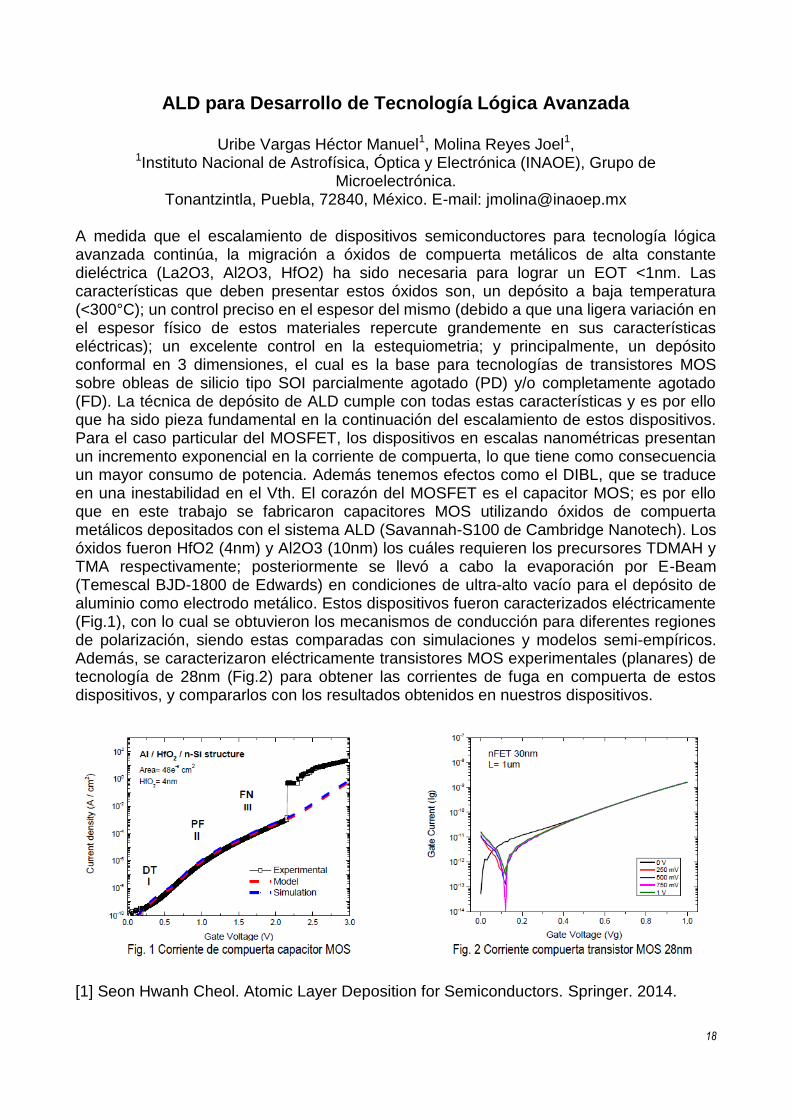
A medida que el escalamiento de dispositivos semiconductores para tecnología lógica avanzada continúa, la migración a óxidos de compuerta metálicos de alta constante dieléctrica (La2O3, Al2O3, HfO2) ha sido necesaria para lograr un EOT <1nm. Las características que deben presentar estos óxidos son, un depósito a baja temperatura (<300°C); un control preciso en el espesor del mismo (debido a que una ligera variación en el espesor físico de estos materiales repercute grandemente en sus características eléctricas); un excelente control en la estequiometria; y principalmente, un depósito conformal en 3 dimensiones, el cual es la base para tecnologías de transistores MOS sobre obleas de silicio tipo SOI parcialmente agotado (PD) y/o completamente agotado (FD). La técnica de depósito de ALD cumple con todas estas características y es por ello que ha sido pieza fundamental en la continuación del escalamiento de estos dispositivos. Para el caso particular del MOSFET, los dispositivos en escalas nanométricas presentan un incremento exponencial en la corriente de compuerta, lo que tiene como consecuencia un mayor consumo de potencia. Además tenemos efectos como el DIBL, que se traduce en una inestabilidad en el Vth. El corazón del MOSFET es el capacitor MOS; es por ello que en este trabajo se fabricaron capacitores MOS utilizando óxidos de compuerta metálicos depositados con el sistema ALD (Savannah-S100 de Cambridge Nanotech). Los óxidos fueron HfO2 (4nm) y Al2O3 (10nm) los cuáles requieren los precursores TDMAH y TMA respectivamente; posteriormente se llevó a cabo la evaporación por E-Beam (Temescal BJD-1800 de Edwards) en condiciones de ultra-alto vacío para el depósito de aluminio como electrodo metálico. Estos dispositivos fueron caracterizados eléctricamente (Fig.1), con lo cual se obtuvieron los mecanismos de conducción para diferentes regiones de polarización, siendo estas comparadas con simulaciones y modelos semi-empíricos. Además, se caracterizaron eléctricamente transistores MOS experimentales (planares) de tecnología de 28nm (Fig.2) para obtener las corrientes de fuga en compuerta de estos dispositivos, y compararlos con los resultados obtenidos en nuestros dispositivos.
[1] Seon Hwanh Cheol. Atomic Layer Deposition for Semiconductors. Springer. 2014.
19
CAD (Computer-Aided Design) para la Fabricación y Caracterización de Dispositivos MOSFET y FinFET con Dieléctricos de Alta-K
Omar López López1, Joel Molina Reyes1.
1Instituto Nacional de Astrofísica, Óptica y Electrónica (INAOE), Grupo de Microelectrónica. Tonantzintla, Puebla, 72840, México. E-mail: [email protected]
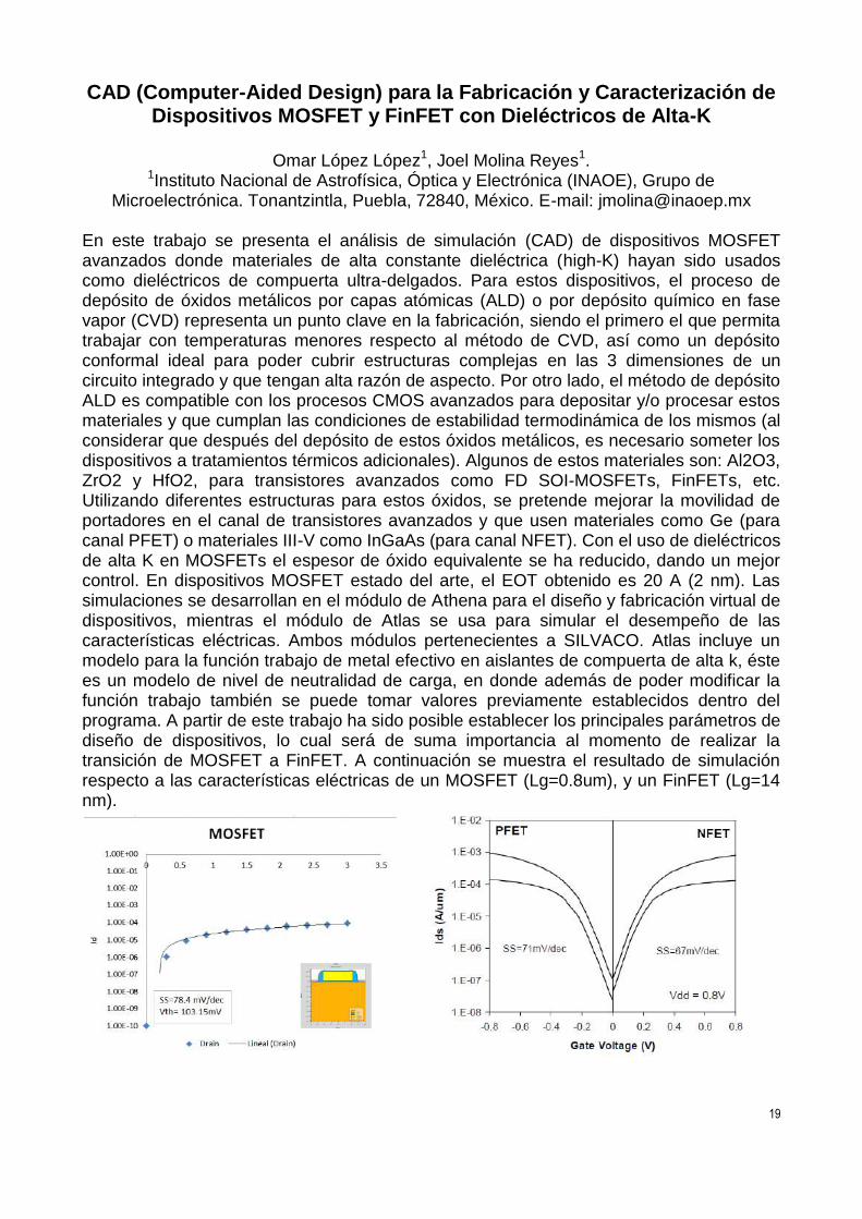
En este trabajo se presenta el análisis de simulación (CAD) de dispositivos MOSFET avanzados donde materiales de alta constante dieléctrica (high-K) hayan sido usados como dieléctricos de compuerta ultra-delgados. Para estos dispositivos, el proceso de depósito de óxidos metálicos por capas atómicas (ALD) o por depósito químico en fase vapor (CVD) representa un punto clave en la fabricación, siendo el primero el que permita trabajar con temperaturas menores respecto al método de CVD, así como un depósito conformal ideal para poder cubrir estructuras complejas en las 3 dimensiones de un circuito integrado y que tengan alta razón de aspecto. Por otro lado, el método de depósito ALD es compatible con los procesos CMOS avanzados para depositar y/o procesar estos materiales y que cumplan las condiciones de estabilidad termodinámica de los mismos (al considerar que después del depósito de estos óxidos metálicos, es necesario someter los dispositivos a tratamientos térmicos adicionales). Algunos de estos materiales son: Al2O3, ZrO2 y HfO2, para transistores avanzados como FD SOI-MOSFETs, FinFETs, etc. Utilizando diferentes estructuras para estos óxidos, se pretende mejorar la movilidad de portadores en el canal de transistores avanzados y que usen materiales como Ge (para canal PFET) o materiales III-V como InGaAs (para canal NFET). Con el uso de dieléctricos de alta K en MOSFETs el espesor de óxido equivalente se ha reducido, dando un mejor control. En dispositivos MOSFET estado del arte, el EOT obtenido es 20 A (2 nm). Las simulaciones se desarrollan en el módulo de Athena para el diseño y fabricación virtual de dispositivos, mientras el módulo de Atlas se usa para simular el desempeño de las características eléctricas. Ambos módulos pertenecientes a SILVACO. Atlas incluye un modelo para la función trabajo de metal efectivo en aislantes de compuerta de alta k, éste es un modelo de nivel de neutralidad de carga, en donde además de poder modificar la función trabajo también se puede tomar valores previamente establecidos dentro del programa. A partir de este trabajo ha sido posible establecer los principales parámetros de diseño de dispositivos, lo cual será de suma importancia al momento de realizar la transición de MOSFET a FinFET. A continuación se muestra el resultado de simulación respecto a las características eléctricas de un MOSFET (Lg=0.8um), y un FinFET (Lg=14 nm).
20
ALD en el Desarrollo de Dispositivos de Memoria No-Volátiles
Emergentes
René Valderrama1, Joel Molina1 1Instituto Nacional de Astrofísica, Óptica y Electrónica (INAOE), Grupo de
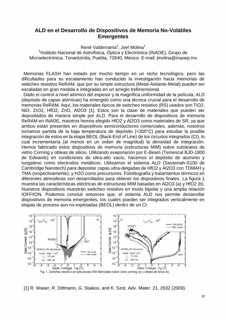
Microelectrónica. Tonantzintla, Puebla, 72840, México. E-mail: [email protected] Memorias FLASH han estado por mucho tiempo en un nicho tecnológico, pero las dificultades para su escalamiento han conducido la investigación hacia memorias de switcheo resistivo ReRAM, que por su simple estructura (Metal-Aislante-Metal) pueden ser escaladas en gran medida e integradas en un arreglo tridimensional. Dado el control a nivel atómico del espesor y la magnífica uniformidad de la película, ALD (depósito de capas atómicas) ha emergido como una técnica crucial para el desarrollo de memorias ReRAM. Aquí, los materiales típicos de switcheo resistivo (RS) usados son TiO2, NiO, ZrO2, HfO2, ZnO, Al2O3 [1]. Estos son la clase de materiales que pueden ser depositados de manera simple por ALD. Para el desarrollo de dispositivos de memoria ReRAM en INAOE, nosotros hemos elegido HfO2 y Al2O3 como materiales de SR, ya que ambos están presentes en dispositivos semiconductores comerciales, además, nosotros tomamos partida de la baja temperatura de depósito (<300°C) para estudiar la posible integración de estos en la etapa BEOL (Back-End of Line) de los circuitos integrados (CI), lo cual incrementaría (al menos en un orden de magnitud) la densidad de integración. Hemos fabricado estos dispositivos de memoria (estructuras MIM) sobre substratos de vidrio Corning y obleas de silicio. Utilizando evaporación por E-Beam (Temescal BJD-1800 de Edwards) en condiciones de ultra-alto vacío, hacemos el depósito de aluminio y tungsteno como electrodos metálicos. Utilizamos el sistema ALD (Savannah-S100 de Cambridge Nanotech) para depositar capas ultra-delgadas de HfO2 y Al2O3 con TDMAH y TMA (respectivamente), y H2O como precursores. Fotolitografía y tratamientos térmicos en diferentes atmosferas son desarrollados para obtener los dispositivos finales. La figura 1 muestra las características eléctricas de estructuras MIM basadas en Al2O3 (a) y HfO2 (b). Nuestros dispositivos muestran switcheo resistivo en modo bipolar y una amplia relación IOFF/ION. Podemos concluir entonces que, el sistema ALD nos permite desarrollar dispositivos de memoria emergentes, los cuales pueden ser integrados verticalmente en etapas de proceso aun no explotadas (BEOL) dentro de un CI.
[1] R. Waser, R. Dittmann, G. Staikov, and K. Szot, Adv. Mater. 21, 2632 (2009).
21
Synthesis and characterization of TiO2 nanofilms by ALD for electric and photocatalytic applications
H. Hernandez-Arriaga
a, E. García-Ramirez
a, M. G. Garcia-Valdivieso
a, P. G. Mani-Gonzalez
b, J.
Molina-Reyesc, Eduardo Martìnez
d, E. López- Luna
a, J.L. Enriquez- Carrejo
b, M.A. Vidal-Borbolla
a.
aCoordinadora para la Innovación y la Aplicación de la Ciencia y Tecnología, UASLP Sierra Leona 550,
Lomas 1ª. Sección, San Luis Potosí, C.P. 78210, San Luis Posotí, México bInstituto de Ingeniería y Tecnología, Departamento de Física y Matemáticas, Universidad Autónoma de
Ciudad Juárez, Ave. Del Charro 450, Cd. Juárez C.P. 32310, Chihuahua., México. cInstituto Nacional de Astrofìsica, Optica y Electronica, Luis Enrique Erro 1 Tonantzintla C.P. 72840, Puebla,
México. dCentro de Investigación en Materiales Avanzados Monterrey, Alianza Norte 202. Parque de Investigación e
Innovación Tecnológica. Apodaca, C.P. 66600, Nuevo León, México.
Abstract
Titanium oxide (TiO2) films are being studied for its high-k constant and photocatalytic properties.
Atomic layer deposition (ALD) is a novel technique used to deposit TiO2 with high quality and
control thickness. Some applications for TiO2 are anti-reflective coatings, sensors and MOSFET´s.
The TiO2 films were synthetized through Titanium Isopropoxide as precursor and H2O as
oxidant-agent varying the aperture-time valve of H2O pulse each ALD cycles. Oxygen vacancies
were created in TiO2 films to perform ferromagnetic measurements. TiO2 films were exposed to
thermal annealing to induce crystallization above 500 °C. X-Ray Reflectivity (XRR) and
transmission electron microscopy (TEM) were used to compare TiO2 nanofilms thickness and
quality obtained through ALD technique. Stoichiometric films were studied with X-Ray
Photoelectron Spectroscopy (XPS). Leakage current and dielectric constant were studied through
I-V, C-V measurements respectively.