advertiment. lʼaccés als continguts dʼaquesta tesi queda...
TRANSCRIPT

ADVERTIMENT. Lʼaccés als continguts dʼaquesta tesi queda condicionat a lʼacceptació de les condicions dʼúsestablertes per la següent llicència Creative Commons: http://cat.creativecommons.org/?page_id=184
ADVERTENCIA. El acceso a los contenidos de esta tesis queda condicionado a la aceptación de las condiciones de usoestablecidas por la siguiente licencia Creative Commons: http://es.creativecommons.org/blog/licencias/
WARNING. The access to the contents of this doctoral thesis it is limited to the acceptance of the use conditions setby the following Creative Commons license: https://creativecommons.org/licenses/?lang=en

Functional oxide films and interfaces: ferroelectric
BaTiO3 films on Si(001) and conducting (110) and
(111) LaAlO3/SrTiO3 interfaces
Mateusz Ścigaj
October 2016
Doctoral Thesis
SUPERVISORS
Dr. Florencio Sánchez Barrera
Dr. Gervasi Herranz Casabona
Institut de Ciència de Materials de Barcelona ICMAB-CSIC
Laboratory of Multifunctional Oxides and Complex Structures
TUTOR
Prof. Javier Rodríguez Viejo
Universitat Autònoma de Barcelona
Department of Physics, Faculty of Science
Doctoral Program: Material Science


Dr. Florencio Sánchez Barrera and Dr. Gervasi Herranz Casabona, tenured
scientists at the Institut de Ciència de Materials de Barcelona - Consejo Superior de
Investigaciones Científicas, and Prof. Javier Rodríguez Viejo, applied physics professor
at Universitat Autònoma de Barcelona
CERITIFY
that Mateusz Ścigaj, master in engineering in chemistry, carried out under their direction
the research work entitled “Functional oxide films and interfaces: ferroelectric BaTiO3
films on Si(001) and conducting (110) and (111) LaAlO3/SrTiO3 interfaces”. This work
has been developed within a PhD program in Materials Science at the Universitat
Autònoma de Barcelona at the department of physics.
For that record they sign the certificate.
Bellaterra, October 2016
Dr. Florencio Sánchez
Barrera
Dr. Gervasi Herranz
Casabona
Prof. Javier Rodríguez
Viejo


v
Acknowledgement
First of all, I would like to send my gratitude to my PhD supervisors, dr. Florencio Sánchez
and dr. Gervasi Herranz, for giving me the opportunity to work with them and for
presenting me the world of physics. Herein, I also would like to thank prof. Josep
Fontcuberta for showing me the right research methodology, always based on logic and
inquisitiveness.
Special thanks go to dr. Nico Dix, for his time spent with me in the PLD RHEED and XRD
laboratories and to dr. Ignasi Fina for the valuable discussions on ferroelectricity and for
the PFM and MFM measurements. I also acknowledge dr. Jaume Gazquez for his work
with TEM and dr. Vassil Skumryev for his work with SQUID. Here I would like to extend
my gratitude to other members of our research group at ICMAB for creating a friendly and
scientifically stimulating environment, namely to: dr. David Pesquera, dr. Diego Gutierrez,
dr. Ekaterina Khestanova, Rafael Cichelero, Liu Fanmao, Blai Casals and dr. Vladimir
Laukhin. Moreover, I would like to express my gratitude to dr. Jean Fompeyrine and dr.
Stefan Abel from IBM Zurich for the valuable collaboration. I also thank all my friends
with whom I was not directly collaborating for the words of encouragements, especially to
dr. Yu Siming and dr. Cornelia Pop.
I also recognise the support of the scientific service at ICMAB, namely the technicians of
AFM, XRD, SEM, PPMS and the clean room.
Jednocześnie chciałbym podziękować moim rodzicom za to, że zawsze byli ze mną.
Chciałbym im podziękować za nieustanną pomoc i motywację do podążania karierą
naukową, pomimo wszelkich przeciwności obecnych w naszych życiach.

Moreover, I could not possibly oversee the vision promoted and the work done by
developers of free software1. This work could not be done in the current shape without
them.
Finally, I would like to acknowledge the financial support for conducting my PhD studies
by means of the AGAUR (Government of Catalonia) and the FPU (Government of Spain)
grants. Further financial support by the Spanish Government (projects MAT2011-29269-
CO3, NANOSELECT CSD2007-00041 and MAT2014-56063-C2-1-R) and the Catalan
Government (2009 SGR 00376) is also acknowledged.
1 Zotero (www.zotero.org), VESTA (jp-minerals.org/vesta/en), Gwyddion (gwyddion.net), WSxM
(www.wsxmsolutions.com), ImageJ (imagej.nih.gov/ij/), ReMagX (remagx.org), MAUD
(maud.radiographema.eu), GIMP (http://www.gimp.org)

vii
Somewhere, something incredible is waiting to be known.
Carl Sagan2
2 This quote is commonly attributed to prof. Carl Edward Sagan, an American astronomer. However, the true
author might actually be Sharon Begley, a Newsweek reporter working on the article with prof. Sagan. [1]


ix
Abstract
In this thesis the focus was aimed to the monolithic integration of functional oxides on
silicon and to the exploration of interfaces between different oxides and the SrTiO3(110)
and SrTiO3 (111) surfaces.
Herein we report the monolithic integration of ferroelectric BaTiO3 on silicon, the current
platform for microelectronics. This was done using the LNO/CeO2/YSZ buffer layer. The
structural and functional properties are investigated. The films are epitaxial an c-oriented.
Very low surface roughness and high ferroelectric remanent polarization are reported. High
crystal quality ferrimagnetic CoFe2O4 was subsequently integrated in the structure. Thus
obtained multifunctional structure shows high structural quality, robust ferromagnetism
and superior ferroelectric properties, all at room temperature. Moreover, we report the
integration of epitaxial BaTiO3 on Si using SrTiO3 buffer layer. Also in this case the
recorded ferroelectric loops point to the good functional properties of this structure. A
structural and functional comparison is given between BTO grown on the thin SrTiO3 and
CeO2/YSZ buffer layers on silicon.
We also report on the structural and transport properties of LaAlO3/SrTiO3 interfaces, with
special emphasis on the LaAlO3/SrTiO3(110) interface featuring two-dimensional electron
gas (2DEG). Further analysis of the interface structure and chemistry, electronic orbital
hierarchy and superconductivity enriched our knowledge of the 2DEG electronic
properties. Special focus also was given to the conductive interfaces comprising
SrTiO3(110), SrTiO3(111) and amorphous oxides. This study enables us to disentangle the
relative importance of the oxygen affinity of the deposited metals and the orientation-
dependent energy of vacancy formation and diffusion on the creation of oxygen vacancies.
In addition we report the layer by layer growth of Y:ZrO2 on SrTiO3(110), leading to the
epitaxial relationship [110]YSZ(001) //[001]SrTiO3(110). This novel idea of an interface
featuring a symmetry discontinuity with the substrate being the lower symmetry material
paves the way towards development of other innovative oxide interfaces.

x
Resumen
La tesis aborda la integración monolítica de óxidos funcionales sobre silicio y la
exploración de intercaras entre SrTiO3(110), SrTiO3(111) y otros óxidos
En primer lugar la tesis detalla la integración monolítica del BaTiO3 en silicio, la plataforma
actual en microelectrónica. Para ello se ha usado la heteroestructura LaNiO3/CeO2/YSZ
como capa de barrera química y acomodación estructural. Se han investigado las
propiedades estructurales y funcionales. Las capas son epitaxiales y orientadas con el eje c
perpendicular al substrato, y presentan rugosidad superficial muy baja y alta polarización
ferroeléctrica en remanencia. El óxido ferrimagnético CoFe2O4 fue integrado seguidamente
en la estructura. La estructura multifuncional obtenida presenta alta calidad estructural, con
excelentes propiedades ferromagnéticas y ferroeléctricas a temperatura ambiente.
Asimismo presentamos la integración de BaTiO3 epitaxial sobre Si usando SrTiO3 como
capa de barrera. También en este caso los ciclos de polarización ferroeléctrica medidos
señalan las buenas propiedades funcionales de la estructura. Se presenta una comparación
de las propiedades estructurales y funcionales de BaTiO3 crecido sobre SrTiO3/Si(001) y
sobre CeO2/YSZ/Si(001).
La segunda parte de la tesis se centra en las propiedades estructurales y de transporte de
intercaras de LaAlO3/SrTiO3, con un especial énfasis en el estudio de la formación de un
gas bidimensional de electrones en la intercara LaAlO3/SrTiO3(110). El análisis de la
estructura y química de la intercara, de su jerarquía orbital electrónica, y de sus propiedades
superconductoras amplían el conocimiento existente de los gases bidimensionales de
electrones en intercaras de óxidos. Se han estudiado también las intercaras conductoras
entre SrTiO3(110), SrTiO3(111) y óxidos amorfos. El estudio ha permitido determinar la
importancia relativa de la afinidad con el oxígeno de los metales depositados y la
dependencia con la orientación de la energía de formación y difusión de vacantes de
oxígeno. Además la tesis detalla el crecimiento monocapa a monocapa de Y:ZrO2 sobre
SrTiO3(110), dando lugar a la relación epitaxial [110]YSZ(001) //[001]SrTiO3(110).
Representa una nueva intercara presentando discontinuidad de simetría sin presentar

variantes cristalinas gracias a usar la superficie de menor simetría como substrato, y abre
paso al desarrollo de otras intercaras originales entre óxidos.

xii
Motivation and Outline
Since its discovery microelectronics has been shaping our lives. However, currently we are
reaching the point when the progress in the field becomes hindered by the intrinsic
limitations of the used technology. In order to overcome these shortcomings, we need to
search for new materials, with novel or improved properties. Promising candidates for this
task are functional oxides. The complex oxides feature properties greatly depending on e.g.
lattice distortions and defects, thus giving scientists a great playground. A crucial step in
applying these materials in commercial devices is their integration with current
microelectronic platform. In the last few decades epitaxial films of the most relevant
functional oxides have been achieved on proper substrates. Also, heterostructures
combining different functional oxides, or with new properties emerging from the interface,
have been achieved. More details on the topic may be found in the Introduction in Chapter
1. However, combining complex oxides with other materials, oxides and other types, still
requires important progress.
The thesis aims progressing in relevant objectives in this field:
Integration of functional oxides on silicon. Here we first focus on the ferroelectric
BaTiO3 grown on Si(001). Section 1.3. gives a short introduction to the ferroelectric
perovskites, i.e. the physics and the challenges in their integration with the silicon
platform. Chapter 2 provides information about the growth and resulting structural and
functional properties of the BTO/LNO/CeO2/YSZ/Si structure. In turn, Chapter 4 is
devoted to the analogous structure, but using a thinner SrTiO3 buffer layer.
Combining oxides in multifunctional epitaxial heterostructures. This aim was to
integrate a ferrimagnetic spinel CoFe2O4 and ferroelectric BaTiO3, while the final
structure should have silicon as the substrate. The structural and functional properties
of the multilayer heterostructure are given in Chapter 3.
Creation of functional interfaces with the orientation different from the usual one. In
this case we present (110) and (111) oriented LaAlO3/SrTiO3 conducting interfaces,
therefore having the orientation different than the most studied conventional (001). A
brief summary of the current state of the art in the two-dimensional electron gases at

xiii
the interfaces with SrTiO3 is given in the Section 1.4. The structural and functional
properties of the epitaxial LaAlO3/SrTiO3 interfaces with the (110) and (111)
orientation are given in Chapter 5. In turn, the particular focus on the analogous
interfaces comprising amorphous oxides was given in Chapter 6.
Employing a single crystalline growth of oxides with crystal symmetry discontinuity at
the interface. At this point we investigate the peculiar case of the layer-by-layer growth
of Y:ZrO2 on SrTiO3(110). The details concerning the growth and samples’ structure is
given in Chapter 7.
The final conclusions and perspectives are given in Chapter 8.

xiv
Contents
CHAPTER 1 INTRODUCTION ......................................................................... 1
1.1. Complex oxides ............................................................................................... 1
1.2. Perovskites ..................................................................................................... 4
1.3. Perovskite ferroelectrics .................................................................................. 6
1.3.1. BaTiO3 ............................................................................................................... 7
1.3.2. Growth of BaTiO3 on silicon ............................................................................. 8
1.3.3. Growth of CoFe2O4 on BaTiO3 ........................................................................ 13
1.4. 2DEG at the interfaces with SrTiO3 .................................................................. 15
1.4.1. SrTiO3 ............................................................................................................. 15
1.4.2. LaAlO3 ............................................................................................................. 17
1.4.3. Crystalline LaAlO3/SrTiO3 systems ................................................................. 18
1.5. YSZ/STO interface .......................................................................................... 24
1.6. Methods ........................................................................................................ 25
1.6.1. Pulsed Laser Deposition ................................................................................. 26
1.6.2. Films growth .................................................................................................. 28
1.6.3. Reflection High Energy Electron Diffraction .................................................. 30
1.6.4. LAO/STO transport measurements ............................................................... 32
1.6.5. Ferroelectric characterization ........................................................................ 34
1.6.6. Other techniques ........................................................................................... 38
CHAPTER 2 FERROELECTRIC BATIO3 ON SILICON ....................................... 41
2.1. Growth of BaTiO3 ........................................................................................... 43
2.2. Structural studies ........................................................................................... 45

xv
2.3. Electric and ferroelectric properties ............................................................... 49
2.4. Conclusions ................................................................................................... 53
CHAPTER 3 COFE2O4/BATIO3 ON SILICON .................................................. 55
3.1. Growth of CoFe2O4 ......................................................................................... 57
3.2. Structural characterization ............................................................................. 58
3.3. Electric and ferroelectric properties ............................................................... 60
3.4. Magnetic properties ...................................................................................... 67
3.5. Magnetoelectric characterization ................................................................... 68
3.6. Conclusions ................................................................................................... 71
CHAPTER 4 FERROELECTRIC BATIO3 FILMS ON SRTIO3/SI(001) .................. 73
4.1. STO/Si virtual substrate ................................................................................. 75
4.2. Growth conditions ......................................................................................... 77
4.3. Structural characterization ............................................................................. 78
4.4. Ferroelectric characterization ........................................................................ 82
4.5. Conclusions ................................................................................................... 85
CHAPTER 5 EPITAXIAL LAALO3 ON SRTIO3(110) AND SRTIO3(111) ............. 87
5.1. Substrate preparation .................................................................................... 90
5.2. Growth of LaAlO3 ........................................................................................... 93
5.3. Transmission electron microscopy studies ...................................................... 97
5.4. Electronic transport at the interfaces ........................................................... 100

xvi
5.5. Electron orbital reconstruction in LaAlO3/SrTiO3(110) ................................... 106
5.6. Electrostatic modulation of superconductivity in LaAlO3/SrTiO3(110) ............ 110
CHAPTER 6 THE INTERFACE BETWEEN AMORPHOUS OXIDES AND
SRTIO3(110) AND (111) .................................................................................. 115
6.1. Growth of the amorphous layers .................................................................. 117
6.2. Electronic transport properties ..................................................................... 118
6.3. Thermodynamic considerations .................................................................... 122
6.4. Electron microscopy studies of the interface ................................................. 123
6.5. The role of oxygen vacancies ........................................................................ 125
6.6. Conclusions .................................................................................................. 127
CHAPTER 7 YSZ(001)/SRTIO3(110): SYMMETRY DISCONTINUITY STUDY .. 129
7.1. Growth conditions ........................................................................................ 131
7.2. In-situ epitaxy studies using RHEED .............................................................. 131
7.3. Further structural and morphological characterization .................................. 134
7.4. Final remarks on the epitaxy of YSZ on STO(110)........................................... 137
CHAPTER 8 GENERAL CONCLUSIONS ....................................................... 139

1
Chapter 1 Introduction
1.1. Complex oxides
Microelectronics is based on semiconductors, materials extensively studied for the last
decades. Currently it is hard to imagine our everyday live without elements like diodes or
transistors. The global semiconductor industry increases its value each year reaching
$335.2 billion in sales in 2015 [2] (Figure 1.1). In order to meet the increasing consumers’
needs for more efficient and cheaper devices, the design becomes more sophisticated.
However, the current technology struggles with its inherent limitations, e.g. the extension
of the Moore’s law (Figure 1.2) via further thinning of the transistor gate dielectric results
in an increased tunneling leakage current, thus leading to high power consumption.
Therefore, the exploration of innovative materials with new functionalities is required.
Figure 1.1 Worldwide semiconductor revenues (3 months moving average). Data obtained from ref. [2].

Chapter 1: Introduction
2
Figure 1.2 (top) visualization of Moore's law for computing, a graph reproduced from ref. [3]; (bottom)
examples of a progress in memory down-scaling across the years.
The discovery of superconductivity in YBa2Cu3O7-x (YBCO) placed oxides into the focus
of wide research. In contrast to the conventional semiconductors, like e.g. Si, Ge or GaAs,
where the interface phenomena are based on s- and p- electrons, the transition metal oxides
involve electrons in narrow d-bands. This in turn promotes the existence of correlated
states, like (two-dimensional) superconductivity and (anti)ferromagnetism, where the
electron system cannot be described by simple particle physics which neglects the
interactions between the charge carriers. On the list of examples of correlated transition
metal oxides we can find among others: cuprates showing high temperature
superconductivity [4], manganites with their colossal magnetoresistance [5] and vanadium
oxide featuring metal-insulator transition (used in a Mott transistor) [6]. These phenomena

Chapter 1: Introduction
3
arise from a nontrivial interplay between spin, charge, orbit and lattice degrees of freedom
(Figure 1.3). In principle, a correlation can be modulated by means of chemical
composition, strain, temperature and/or applied fields, thus allowing tuning the materials
properties to specific needs. Moreover, the constituting transition metal can have different
valence states (e.g. Ti3+, Ti4+). This degree of freedom opens a way to electronic
reconstruction at the surfaces and interfaces, apart from the structural reconstruction known
from conventional semiconductors. Complex oxides stabilize in many crystal structures,
often allowing the existence of properties like (anti)ferroelectricity and
(anti)ferromagnetism. The modulation of cation ratio in solid solution, the possibility of
doping by oxygen vacancies and the chemical stability in generally wide span of
temperatures bring about a possible existence of complex phase diagrams with unique
properties. Having all this in mind, there should be no doubt why functional complex oxides
are now main candidates as emerging materials in the International Technology Roadmap
for semiconductors (ITRS)3.
Figure 1.3 Electronic and structural degrees of freedom in correlated oxides. A diagram reproduced from
ref. [7].
3 ITRS is a set of documents elaborated by a group of semiconductor industry expert with the aim to give the
best opinion on the direction of research in the related areas of technology. http://www.itrs2.net/

Chapter 1: Introduction
4
Among complex oxides a very important group is a structural family of perovskites.
Compounds of this class are of key importance mainly due to their wide range of properties
and fairly similar unit cell parameters making possible a growth of multilayer structures.
The following Section 1.2. gives a brief overview on this family.
1.2. Perovskites
ABX3 is the general chemical formula of a perovskite, where A and B denote cations (the
cation A is somehow bigger than the cation B), while X stands for an oxygen or a halogen
anion. For the compounds used in this thesis the X anion is always oxygen, therefore from
now on we will be refereeing to perovskites as ABO3. The perovskite structure can be
described as a network of corner shared BO6 octahedra with the A cation being in 12-fold
cuboctahedral coordination (Figure 1.4).
Figure 1.4 A perovskite structure ABX3 depicted as having in the center a BO6 octahedron (left) or an AO12
cuboctahedron (center).
Perovskites are a very diverse group of compounds due to the fact that the generic structure
can underwent many alternations. The degrees of freedom include e.g. a choice of the
constituting cations and an ability to accommodate fairly high amount of vacancies. The
ABO3 compounds can crystalize in many systems, like cubic, tetragonal, orthorhombic,
rhombohedral and monoclinic. Moreover, phase transitions induced by a change in
temperature or pressure are common. This richness of chemistry is reflected in the presence
of variety of physical properties. [8] The perovskite compounds can be insulating,
semiconductive, metallic, superconductive, piezoelectric, ferroelectric, magnetic and

Chapter 1: Introduction
5
multiferroic. They are important also from the chemical point of view as materials for
energy storage and conversion systems and catalysis. [9,10]
Figure 1.5 Functionalities of perovskite oxides as bulk and interface phenomena. Figure reproduced from
ref. [8].
As mentioned in the previous Section, one way to make a further progress in the field of
microelectronics is to employ new materials in devices. A good example of this is the use
of ferroelectric materials, like BaTiO3, as a high-κ gate dielectrics in a MOSFET4 yielding
a ferroelectric field effect transistor, which has both the memory and the logic
functionality. [11] Other possibility is to integrate a few layers of different materials, which
in turn can bring new properties (like e.g. multiferroicity in BaTiO3/CoFe2O4) or enhance
the ones already present in one of the layers (like e.g. the enhanced ferroelectricity in
BaTiO3/SrTiO3/CaTiO3 superlattices [12] or enlarged supercurrent density in YBa2Cu3O7-
δ/Y1-xCaxBa2Cu3O7-δ [13]). In a multilayer structure a key role in the device functionality
may be played by the interface rather than by the bulk properties of the constituting
materials. A great example for this in the world of oxides is the LaAlO3/SrTiO3 interface
4 MOSFET stands for Metal–Oxide–Semiconductor Field-Effect Transistor; it is the most common transistor
type in both digital and analog circuits. High-κ (dielectric constant) materials enables lower operating voltage.

Chapter 1: Introduction
6
featuring insulator-to-metal transition, which can be triggered electrostatically, giving a
chance to created nanometric size transistors. [14]
In the following Section 1.3. we will shortly discuss the physics of ferroelectrics and
explain the main challenges in their integration on the key substrate of current
microelectronics – silicon. The subsequent Section 1.4. will be devoted to the conduction
at the LaAlO3/SrTiO3 interfaces, where certain experimental findings and proposed
theoretical models will be brought up.
1.3. Perovskite ferroelectrics
Ferroelectric materials are those which possess a spontaneous polarization (i.e. existing
even without applying an external electric field) and where this polarization5 can be
switched by an application of an electric field. These materials are also pyroelectric and
piezoelectric, which means that a change in the polarization can be induced by a variation
of temperature and strain, respectively. Ferroelectricity was for the first time reported in
1921 for a Rochelle salt (KNaC4H4O6·4H2O) [15], where hydrogen bonds rely on the origin
of this property [16]. The discovery in 1945 of ferroelectricity in BaTiO3 [17], a simple
inorganic perovskite compound, has triggered a more extended research on this family of
compounds. Nowadays, the perovskite ferroelectrics are still the most studied group.
Perovskite ferroelectric oxides, like e.g. Pb(ZrxTi1-x)O3, Bi4Ti3O12, and BaTiO3, have been
intensively investigated due to the interest of using them in many devices. Here, to name
just a few, we can mention: non-volatile random access memories, MEMS, optoelectronic
devices and energy storage devices. [18–20] Apart from the functional properties of the
material, one should also keep in mind the manufacturing and the everyday handling
process. In general, it is preferred to avoid a vacuum deposition of materials containing
volatile elements, like Bi of Pb, as they constitute a possible origin of a contamination of
the deposition chamber, a cross-contamination of other materials and an off-stoichiometry
5 Polarization can be defined as a vector field that expresses the density of electric dipole moments in a
dielectric material. For somehow more practical purposes, polarization can be related with the density of an
electric charge developed on the surface of the dielectric.

Chapter 1: Introduction
7
of the grown film. Moreover, Pb is a toxic element and policies of many countries are aimed
towards the removal of Pb-containing products from the marked. [21–24]
1.3.1. BaTiO3
BaTiO3 (for short BTO) is one of the most studied ferroelectric compounds due to its good
ferroelectric properties (remanent polarization of Pr ≈ 26 µC/cm2), good electro-optical
properties (effective Pockels coefficient of reff ≈ 148 pm V-1), simple chemical composition
and the fact that it is Bi- and Pb-free.
BTO undergoes a few phase transitions depending on the temperature. At the temperatures
above ≈ 120 °C is cubic; this is a paraelectric phase (i.e. without a spontaneous dipole
moment). Below this temperature the arrangement of atoms changes into one of the lower
symmetry lattice systems and the material becomes ferroelectric with given direction of the
polar axis. Upon cooling the bulk material at ≈ 120 °C becomes tetragonal (with the polar
axis P along the [001] direction), at ≈ 0 °C orthorhombic (P || [011]) and at ≈ -90 °C
rhombohedral (P || [111]). Therefore, at about the room temperature bulk BTO is tetragonal
(space group P4mm) with the cell parameters c = 4.038 Å and a = b = 3.994 Å (see Figure
1.6 for the visualization of the atomic displacement – the origin of the dipole moment).
Figure 1.6 A unit cell of BTO sketched with atomic radii. The atomic coordinates were taken from ref. [25].

Chapter 1: Introduction
8
1.3.2. Growth of BaTiO3 on silicon
Despite the vast amount of interesting functional properties of BTO, its applicability in
microelectronic devices is hindered due to the difficulties in its monolithic integration with
the silicon platform. The problem is common also in the growth of other complex oxides
on silicon and includes the chemical stability and structural compatibility issues.
A direct growth of oxides on a silicon substrate is also very relevant for technological
applications. For instance, the direct growth of high-κ materials is an important strategy
towards further miniaturization of MOSFETs. In the ideal case, oxides would growth
directly on a silicon substrate yielding an atomically sharp interface. However, it is often
not the case and an additional phase arises at the interface (see examples in Figure 1.7).
One reason for this might be the negative change of Gibbs free energy for the chemical
reactions between silicon and a deposited oxide. [29,30] Apart from pure thermodynamics
of chemical reactions between bulk materials, other factors may play a role, like e.g. energy
of the interface between a thin film material and the substrate, the occurrence of chemical
reactions involving gaseous species and the influence of kinetic barriers. [31,32] In overall,
it is often found experimentally that: the high oxygen pressure used during growth leads to
Figure 1.7 Different types of interfaces of oxides with silicon; the illustrative TEM images were taken from
the literature, respectively: silicon oxide [26], silicate [27], silicide [28].

Chapter 1: Introduction
9
an interfacial SiOx layer, the use of reducing conditions to silicide, while silicates are often
found during deposition of rare-earth oxides.
Another difficulty arises from a mismatch between thermal expansion coefficients of
silicon and complex oxides. For instance for BTO αBTO,RT = 6.1·10-6 K-1, while for silicon
this value is only αSi,RT = 2.3·10-6 K-1. [33] This discrepancy may have profound
consequences upon cooling of the structure after the deposition. [34,35] The resulting high
residual tensile stress may cause cracks in the film. Moreover, as BTO lowers its symmetry
from cubic into tetragonal, a few orientations of the domains are possible (Figure 1.8) with
different orientation of the polar c-axis. Although BTO films with in-plane polarization are
desirable for many electro-optical applications [36,37], BTO with out-of-plane polarization
is required for e.g. ferroelectric memory devices [38], neuromorphic computing [39] and
quantum computing [40] architectures. Nevertheless, the mechanical clamping of BTO thin
film with the Si substrate -nominally causing a tensile stress- should promote the presence
of a-domains. Consequently, the epitaxial growth of c-oriented BTO on Si(001) is
challenging.
Figure 1.8 Different possible orientations of tetragonal BTO on a substrate.
The epitaxial growth of complex oxides on silicon is usually achieved by the use of buffer
layers. A buffer is a material grown epitaxially on silicon; this layer is further used as a
virtual substrate (a template) for a subsequent growth of other films. Already a high number
of crystalline oxides can be grown directly on silicon [41], making up possible buffer
layers. Today, the most important compounds for this purpose are SrTiO3 (STO) and
Y:ZrO2 (YSZ). In fact, already both STO [42] and YSZ [43] have been successfully used
for the integration of high quality ferroelectric Pb(Zr,Ti)O3 on silicon. As on this substrate
STO is grown by means of molecular beam epitaxy (MBE), while YSZ is prepared by

Chapter 1: Introduction
10
pulsed laser deposition (PLD), the use of the buffer layer finally depends on the deposition
technique available in the laboratory. Below we will shortly present the most widely used
buffers for the growth of BTO on Si.
At the end of the 90’s researchers from Oak Ridge National Laboratory achieved an
epitaxial growth of STO on silicon with an atomically flat interface. [44] The strategy used
by them relied on the deposition by MBE of alkaline metals (as Sr) on a bare Si(001); in
this case the resulting SrSi2 permitted subsequent growth of SrO and STO. This finding has
started the use of STO as a buffer layer on silicon. The later protocol modifications by
Motorola [45,46] enabled the growth of STO with high crystalline quality and flat surface
even with no interfacial SiO2 layer. In any case, the deposition of STO on Si requires a very
accurate control of oxygen pressure and temperature. By now, only a few groups have
reported c-oriented epitaxial BTO on STO/Si(001) [36,47–54] and none of these papers
reports a ferroelectric polarization loop as a direct proof of ferroelectricity.
The other buffer commonly used in the growth of complex oxides on Si(001) is YSZ. This
material is generally grown by means of PLD resulting in a flat surface and an almost SiOx-
free interface. In order to achieve the high quality buffer, YSZ initially is grown on as-
received silicon substrate at ultra-high vacuum or at very low oxygen pressure and
temperature T ≈ 800 °C. Under these conditions the deposited Y and Zr reduce the native
silicon oxide yielding an epitaxial thin layer of YSZ (see Figure 1.9). [55] Further growth
of YSZ is conducted at low oxygen pressure, suitable for growth of this oxide. As this
material features high oxygen permeability, at high temperatures oxygen from the
deposition chamber diffuses through it to the silicon substrate resulting in a thin layer of
amorphous SiOx. This buffer structure was used in the integration of BaTiO3(110)/SrRuO3
bilayers on silicon microcantilevers, with possible future applications in
microelectromechanical systems. [56] Moreover, very recently good ferroelectric
properties of BTO grown on silicon have been reported for a complex
YSZ/SrOx/STO/LSMO buffer structure. [57]
Yet another strategy is based on growing directly on silicon a buffer layer, which at the
same time can serve as an electrode. One example is a very thick layer of LaNiO3. In this
case the growth of c-oriented BTO was achieved. The reported ferroelectric loops indicate
a high remanent polarization of up to around Pr = 10 µC/cm2. [58] On the down side, apart
from the usual overall high thickness of the BaTiO3/LaNiO3 bilayer, the films are very

Chapter 1: Introduction
11
rough [33,59–61] and show a polydomain structure with both the a- and c-domains [58,62–
64]. Such microstructure typically causes leakage and fatigue in ferroelectric films and
therefore, this solution seems to be impractical in commercial devices. Similarly, the use
of other conducting oxide CaRuO3 yields rough and polycrystalline BTO. [65] In addition
many reports have been devoted to the growth of BTO on the Pt-metallized Si(001)
substrate. However, also in this case the films show polycrystallinity or high
granularity. [66–68,61,63] Here, another problem is the low thermal stability of Pt at the
temperatures used for oxides deposition, [66,69,70] and a proper choice of an adhesion
interlayer between Pt and silicon plays a main role [71].
The BaTiO3 layers grown by us (described in Chapter 2) and BaTiO3/CoFe2O4 bilayers
(Chapter 3) are based on the YSZ buffer. This is due to the high quality of the YSZ/Si
virtual substrate and the availability of the pulsed laser deposition technique in our
laboratory. In addition, in Chapter 4 we present the structural and ferroelectric properties
of BTO samples we have grown on the STO/Si platform. An advantage of this buffer is the
possibility of using the overall lower process temperature, approaching the maximum
temperature compatible with CMOS processes, usually being an asset in industry. All the
Figure 1.9 The growth mechanism of YSZ on a silicon substrate. The representative TEM image of the
YSZ/Si interface was taken from [72].

Chapter 1: Introduction
12
above-mentioned structures, grown on either YSZ/Si or STO/Si, contain LaNiO3 as the
bottom electrode, as described below.
In order to investigate the functional properties of our BTO films we need to growth them
in between two electrically conductive layers, i.e. electrodes. The choice of electrodes is
very important, as it will influence the electrical and ferroelectric properties of the studied
material, and in the particular case of the bottom electrode also the film structure. The
electrode materials used for epitaxial growth can be roughly divided into three groups:
noble metals (e.g. Pt, Au, Ir, Ru), conductive rutile-type metal oxides (e.g. IrO2, RuO2) and
conductive perovskite oxides (e.g. LaNiO3, (La,Sr)CoO3, (La,Sr)MnO3, SrRuO3,
YBa2Cu3O7-x). Among them, LaNiO3 (for short LNO) is our bottom electrode of choice,
combining: good lattice matching with BTO, simple structure and the fact that in the wide
temperature range (between 1 - 1000 K) it is metallic, but still paramagnetic and does not
undergo any phase transition. [73] This enables the epitaxial growth of BTO and does not
interfere with ferroelectric nor magnetic measurements at these temperatures. In addition,
this complex oxide has a thermal expansion coefficient of αLNO,RT = 12.9·10-6 K-1 [33], thus
more than BTO. Its eventual relaxation during cooling down from deposition temperature,
if occurred, would reduce the tensile stress on BTO due to its thermal mismatch with the
silicon substrate.
While growth of the BTO/LNO perovskite bilayer on the STO perovskite buffer is not
burdened with large lattice mismatch, the use of the fluorite YSZ buffer is more challenging
(Table 1 lists the lattice mismatch). To overcome this difficulty an additional buffer layer
6 In this thesis the lattice mismatch will be defined as f = (ab – au)/au, where au and ab are the relaxed lattice
constants of the upper and bottom layers, respectively. [74]
Table 1 Bulk lattice parameter of BTO (“a” parameter), LNO, CeO2, YSZ and Si, and lattice mismatch6
(“f”) respect to the closest bottom layer.
Chapter 1: Introduction
13
of CeO2 was used, thus resulting in the final BTO/LNO/CeO2/YSZ/Si(001) heterostructure.
The used complex buffer structure between the functional BTO and the YSZ/Si template
allows a progressive accommodation of the huge lattice mismatch of -8.9 %, which
otherwise could result in a full plastic relaxation and polycrystallinity of BTO.
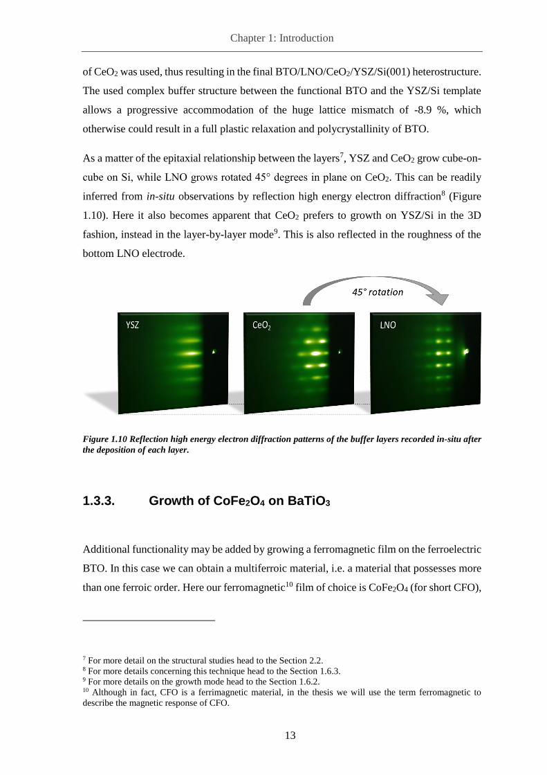
As a matter of the epitaxial relationship between the layers7, YSZ and CeO2 grow cube-on-
cube on Si, while LNO grows rotated 45° degrees in plane on CeO2. This can be readily
inferred from in-situ observations by reflection high energy electron diffraction8 (Figure
1.10). Here it also becomes apparent that CeO2 prefers to growth on YSZ/Si in the 3D
fashion, instead in the layer-by-layer mode9. This is also reflected in the roughness of the
bottom LNO electrode.
Figure 1.10 Reflection high energy electron diffraction patterns of the buffer layers recorded in-situ after
the deposition of each layer.
1.3.3. Growth of CoFe2O4 on BaTiO3
Additional functionality may be added by growing a ferromagnetic film on the ferroelectric
BTO. In this case we can obtain a multiferroic material, i.e. a material that possesses more
than one ferroic order. Here our ferromagnetic10 film of choice is CoFe2O4 (for short CFO),
7 For more detail on the structural studies head to the Section 2.2. 8 For more details concerning this technique head to the Section 1.6.3. 9 For more details on the growth mode head to the Section 1.6.2. 10 Although in fact, CFO is a ferrimagnetic material, in the thesis we will use the term ferromagnetic to
describe the magnetic response of CFO.

Chapter 1: Introduction
14
an insulating material with M = 3 µB/f.u., Néel temperature Tc ≈ 520 °C and a large
magnetostrictive coefficient. [75] CFO has a spinel crystal structure with the unit cell
parameter a = 8.392 Å.
Despite suitable physical properties, high quality growth of CFO on BTO constitutes a
challenge due to the structural dissimilarities. The ideal crystal structure of a spinel has a
close-packed faced centered cubic (fcc) oxygen sublattice with interstitial tetrahedral (A)
and octahedral (B) sites occupied by di- and tri-valent cations (see Figure 1.11 (a)). The
unit cell contains 8 formula units and is much larger than the perovskite one. CFO has as-
called inverse structure, where divalent M 2+ cations are found at B-sites and trivalent N +3
cations are equally distributed over A and B sites; this gives the general formula (N 3+)A [M
2+N 3+]BO4. Moreover, CFO with its large a/2 = 4.196 Å should grow under a significant
compressive epitaxial stress over a c-oriented BTO (lattice mismatch -4.81 %).
Figure 1.11 Structure and morphology of spinels: (a) a schematic CFO unit cell with inverse spinel
structure [76], (b) SEM image of a 111-facetted pyramidal islands in a (001)-oriented CoCr2O4 film
grown on a MgAl2O4(001) substrate. [77,78]
Yet another challenge in achieving flat epitaxial CFO on BTO(001) is overcoming the
thermodynamic limitation of growing (001)-oriented spinels. The surface energy γ in this
case is highly anisotropic (γ(001) ≈ 10·γ(111)) [79], thus the film prefers to grow in the form
of 111-facetted pyramids leading to a rough surface (see an example corresponding to

Chapter 1: Introduction
15
CoCr2O4 on the (b) panel in Figure 1.11). In order to suppress the 3D growth mode, we
have deposited the CFO films under the conditions of kinetic limitation. [80]
1.4. 2DEG at the interfaces with SrTiO3
As we go down with the size of a device, the physics at the surfaces and interfaces have a
predominant role. In many cases the useful functionality of a complex structure relies on
the charge transport along or across an interface, like e.g. in case of p-n junctions in
semiconductor devices. This situation was accurately described by the Nobel laureate H.
Kroemer who said: “Often, it may be said that the interface is the device.” [81] Here it is
important to point out that interface may largely vary from the bulk of the material. First of
all, at an interface the translational symmetry is broken, which may drive to atomic or
electronic reconstructions and eventually can also alter the crystal fields felt by ions in the
lattice. In addition, many defects, like e.g. point defects and dislocations, tend to have
higher density at an interface. Finally, interfaces and surfaces are more prone to changes in
chemical composition. All of this may substantially alter the electronic band structure of
bulk materials allowing the exploitation of surface and interface effects to design devices
for new applications.
The current Section 1.4. is devoted to the LaAlO3/SrTiO3 interface, for which an
unexpected interface conductance was first reported by A. Ohtomo and H.Y. Hwang in
2004 [82]. Despite the fact that the bulk constituting materials are band insulators, the
interface is conductive for certain interface atomic compositions. Subsequently, other
phenomena, e.g. superconductivity and ferromagnetism were also reported for this interface
by different groups.
1.4.1. SrTiO3
Due to its appearance similar to diamond, strontium titanate SrTiO3 (usually abbreviated to
STO) was used as a gemstone between 1950-1970 (see Figure 1.12). The fact that STO has
a “fire” (light dispersion) greatly exceeding that of diamond made it especially appealing

Chapter 1: Introduction
16
for jewels and ornaments. In spite of that, the Mohs hardness of just 5.5 makes it unpractical
in everyday jewelry, which may explain the decline over the years for these applications.
Figure 1.12 STO cut and polished as diamond (left), the same crystal after reduction (right) – the removal
of oxygen atoms from the surface makes it conductive and thus opaque. Pictures taken from [83].
Nowadays STO is particularly important as a substrate for many oxides. This is mainly due
to similarities in the structure and the lattice parameter as well as relatively small reactivity
upon a deposition of an overlayer thin film. The possibility of producing good quality single
crystals at affordable prices is another key aspect making STO the substrate of choice for
many structures. Examples of epitaxially grown functional oxides include ferroelectrics
(perovskites), conductive oxides (nickelates and ruthenates), high temperature
superconductors (curates), colossal magnetoresistance materials (manganites) and
insulating buffer layers (fluorites).
At ambient conditions STO adopts a cubic perovskite structure (space group Pm-3m) with
the cell parameter of 3.905 Å. Below 105 K it adopts a tetragonal structure (space group
I4/mcm) with slightly rotated TiO6 octahedra around the z axis (up to 2.1° at 4.2 K). This
is the so-called tetragonal antiferrodistortive (AFD) phase, in which the original cubic unit
cell is deformed according to the c/a ratio, which can reach ~1.0009 at 10 K.
Stoichiometric STO has an indirect band gap of 3.25 eV and is a band insulator. For the
purpose of comparison, we remind that the semiconducting intrinsic silicon has an indirect
bang gap of about 1.12 eV at room temperature. Introducing oxygen vacancies into the
Chapter 1: Introduction
17
structure of STO increases the charge densities leading to a metallic or even
superconductive state, the latter having its maximum transition temperature Tc (< 500 mK)
at the doping level 1019 – 1021 cm-3 [84]. The metallic state can be reached also by different
ionic substitutions, e.g. Nb for Ti or La for Sr [85], which is used to produce a commercially
available Nb:SrTiO3 substrate which shows n-type conductivity.
STO is an incipient ferroelectric maintaining its paraelectric phase down to T 0 K [86]
However, strain can stabilize a ferroelectric phase even at room temperature. [87] Single‐
crystal single‐domain STO has static dielectric constant ranging from a few hundred at
room temperature [88,89]. Due to its high permittivity STO can be used as agate dielectric
in field effect devices.
1.4.2. LaAlO3
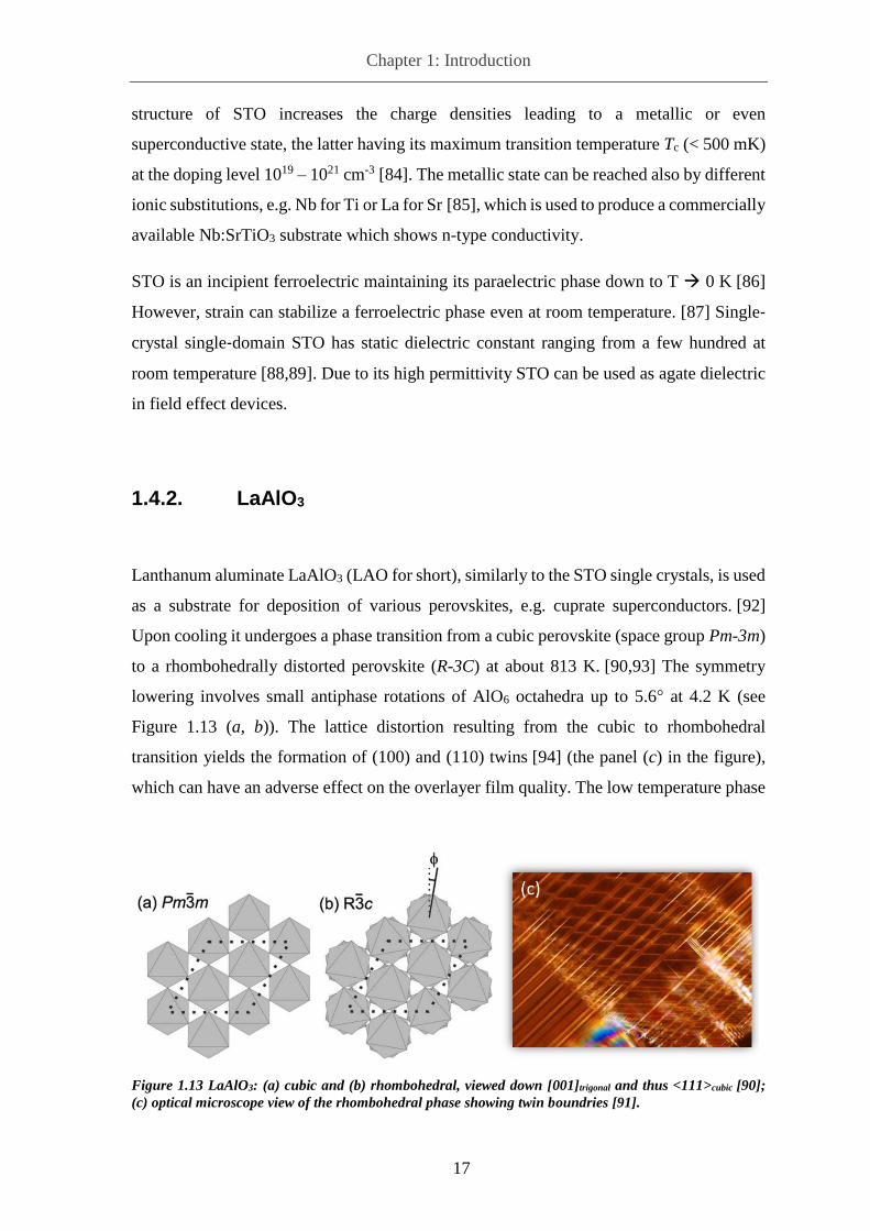
Lanthanum aluminate LaAlO3 (LAO for short), similarly to the STO single crystals, is used
as a substrate for deposition of various perovskites, e.g. cuprate superconductors. [92]
Upon cooling it undergoes a phase transition from a cubic perovskite (space group Pm-3m)
to a rhombohedrally distorted perovskite (R-3C) at about 813 K. [90,93] The symmetry
lowering involves small antiphase rotations of AlO6 octahedra up to 5.6° at 4.2 K (see
Figure 1.13 (a, b)). The lattice distortion resulting from the cubic to rhombohedral
transition yields the formation of (100) and (110) twins [94] (the panel (c) in the figure),
which can have an adverse effect on the overlayer film quality. The low temperature phase
Figure 1.13 LaAlO3: (a) cubic and (b) rhombohedral, viewed down [001]trigonal and thus <111>cubic [90];
(c) optical microscope view of the rhombohedral phase showing twin boundries [91].

Chapter 1: Introduction
18
can be indexed as a pseudocubic perovskite with the lattice parameter of a = 3.791 Å. This
gives a lattice mismatch between LAO and STO of about 3%, which is high, but still
permits achieving a good epitaxy.
Concerning the electronic properties, LAO is a band gap insulator with the energy gap of
5.6 eV and has a dielectric constant of around 24 from room temperature down to 4
K [95,96]. This places it among high-κ oxides; however due to its reactivity with silicon at
high temperatures its application in this field is limited. [97]
1.4.3. Crystalline LaAlO3/SrTiO3 systems
As stated above, sometimes the most interesting phenomena happen at the interface. A great
example of this is the LaAlO3/SrTiO3 interface. This structure was placed in the spot light
by a Nature publication of 2004 by A. Ohtomo and H. Y. Hwang. [82] In the manuscript it
was shown that the interface between the two wide-bandgap insulators exhibits metallic
conductivity, with free electrons being the charge carriers. The epitaxial growth of LAO on
(001)-oriented STO was achieved by pulsed laser deposition. At this orientation the STO
substrate can be terminated by a TiO2 or a SrO layer. Interestingly, a conductive interface
could be achieved only in the case of a TiO2-terminated substrate (see Figure 1.14) [98], a
fact that has been confirmed by all experiments reported so far. It is well established that
the conductivity originates from free electrons localized in a thin layer of STO in a close
proximity of the interface. [99–101] Therefore, we use a term two-dimensional electron gas
(for short 2DEG).
Afterwards other properties of the LAO/STO(001) structure were reported, like a tunable
metal-insulator transition [102], magnetism [103], electrostatically modulated 2D
superconductivity [104] or room temperature giant persistent photoconductivity [105].
These unexpected findings have triggered a huge research on this topic, which is not
expected to fade soon.

Chapter 1: Introduction
19
After over 10 years from the discovery, the origin of 2DEG at the LAO/STO interface is
still debated, although the most accepted mechanism is the polar catastrophe scenario,
proposed in the first publication on the topic [82].
The polar catastrophe scenario takes into account that the n-type conductivity has been
found at the interface between TiO2-terminated STO(001) and epitaxially grown LAO(001)
of a thickness above tc = 4 u.c. of LAO (about 1.52 nm). [106] Using SrO-terminated
substrate results in insulating interface (i.e. room temperature resistance above 109 Ω); the
interfaces are also insulating when the LAO layer is thinner than the critical thickness tc.
To understand the proposed mechanism, we have to take a look at the ideal atomic stacking
at the LaO/TiO2/SrO and LaO/AlO2/SrO interfaces (see Figure 1.15). A generic perovskite
of the formula ABO3 along the [001] direction is composed of alternating layers: AO and
BO2. In the case of STO it means SrO and TiO2 layers. Both of them carry zero net charge
(are neutral) due to the formal charges Ti4+, Sr2+, O2-. On the contrary, in the case of LAO
we have alternating plates LaO+ and AlO2-, which are charged. This results in a polarity
discontinuity at the interface. By integrating the Poisson’s equation for the two systems we
can see that the electrical potential increases monotonically from the interface across the
LAO overlayer. This situation is not favorable energetically. The polar catastrophe scenario
is also known for heterointerfaces between classical semiconductors, e.g.
GaAs/Ge(110) [107]. There, the way to lower system energy is an atomic reconstruction at
the interface. This redistributes the charges of the atomic layers causing an electrical field
Figure 1.14 A sketch of two possible stackings of LAO/STO(001) within an ideal ionic limit. The
LaO/TiO2/SrO (left) results in a conductive structure, while the LaO/AlO2/SrO (right) not.
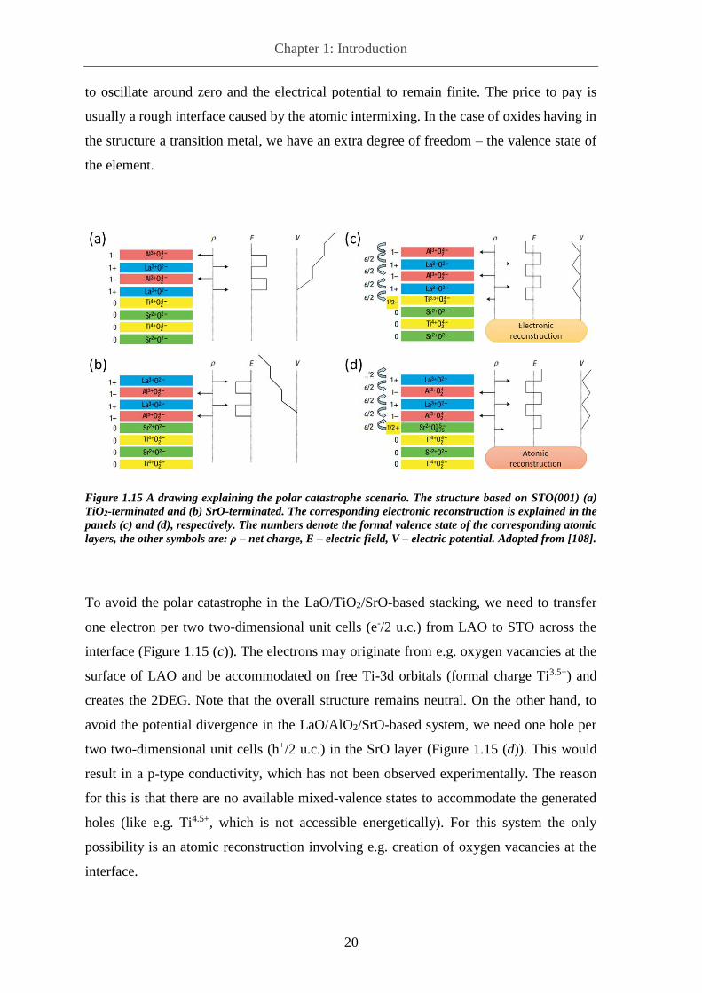
Chapter 1: Introduction
20
to oscillate around zero and the electrical potential to remain finite. The price to pay is
usually a rough interface caused by the atomic intermixing. In the case of oxides having in
the structure a transition metal, we have an extra degree of freedom – the valence state of
the element.
Figure 1.15 A drawing explaining the polar catastrophe scenario. The structure based on STO(001) (a)
TiO2-terminated and (b) SrO-terminated. The corresponding electronic reconstruction is explained in the
panels (c) and (d), respectively. The numbers denote the formal valence state of the corresponding atomic
layers, the other symbols are: ρ – net charge, E – electric field, V – electric potential. Adopted from [108].
To avoid the polar catastrophe in the LaO/TiO2/SrO-based stacking, we need to transfer
one electron per two two-dimensional unit cells (e-/2 u.c.) from LAO to STO across the
interface (Figure 1.15 (c)). The electrons may originate from e.g. oxygen vacancies at the
surface of LAO and be accommodated on free Ti-3d orbitals (formal charge Ti3.5+) and
creates the 2DEG. Note that the overall structure remains neutral. On the other hand, to
avoid the potential divergence in the LaO/AlO2/SrO-based system, we need one hole per
two two-dimensional unit cells (h+/2 u.c.) in the SrO layer (Figure 1.15 (d)). This would
result in a p-type conductivity, which has not been observed experimentally. The reason
for this is that there are no available mixed-valence states to accommodate the generated
holes (like e.g. Ti4.5+, which is not accessible energetically). For this system the only
possibility is an atomic reconstruction involving e.g. creation of oxygen vacancies at the
interface.

Chapter 1: Introduction
21
Despite the fact that the polar catastrophe model seems to explain well the insulating nature
of the LaO/AlO2/SrO interface as well as the critical thickness of the LAO film for the onset
of conductivity at the LaO/TiO2/SrO interface [109], there are certain experimental
findings not fitting well in this simple picture. The theory predicts at the interface the
presence of the charge carrier density equivalent n = 0.5 e- /SSTO(001) ≈ 3.28·1014 cm-2
(SSTO(001) is the area of one 2D unit cell of STO(001), equal 3.9052 Å2). Nevertheless, the
Hall measurement transport data indicate a lower value of the order of 1013. Moreover, the
expected internal electric field across LAO has been found to be much lower than resulting
from the theory [110]. On the other hand, these discrepancies arise from the simplest model,
assuming presence of an atomically sharp defect-free interface. In fact, it has been observed
that atomic intermixing occurs at the LAO/STO(001) interface. One should bear in mind
that the interface disorder can have strong impact on charge profile and the electronic band
structure. [111–113]
Other possible scenarios include cationic intermixing or the presence of oxygen vacancies
at the interface. The intermixing mechanism is based on the fact that the LAO/STO
interface has been found to feature certain interdiffusion [108,114,115] and the fact that the
La1−xSrxTiO3 solid solution is metallic for the wide doping range of 0.05 < x <
0.95 [116,117]. On the other hand, it is known that oxygen vacancies act as electron donors
and that they can be introduced in STO upon heating the substrate at low oxygen
pressure. [118] However, neither intermixing nor the oxygen vacancy model seems to
easily explain the tc = 4 MLs, neither the insulating state of the LaO/AlO2/SrO interface.
Furthermore, sintering LAO and STO compound results in an insulating
material [109,119], while the annealing does not eliminate the metallic conductivity from
the LaO/TiO2/SrO interface [118]. Upon considering different atomic arrangements in
order to understand the origin of the reach physics at the LaO/TiO2/SrO-based interface,
probably it should be pointed out that the very interface is composed of a one unit cell
LaTiO3 (at least within ideal ionic limit). Stoichiometric LaTiO3 is a Mott-insulator [120],
and thus a correlated material, in contrary to STO and LAO.
At the time of the beginning of the thesis, there were no reports discussing 2DEG at
interfaces with STO of an orientation different than the (001). One reason for this might be
a strong believe in the polar catastrophe scenario, which relies on a presence of polarity
discontinuity at the interface, like in the case of LAO(001)/STO(001). In contrast, the

Chapter 1: Introduction
22
heterostructures built by the growth of perovskite oxides on STO(110) do not exhibit any
polarity discontinuity within an ideal ionic limit (see Figure 1.16). This is due to the fact
that perovskites, having a general formula ABO3, along the <110> direction are composed
of alternating layers [O2]4- and [ABO]4+. The formal valence of each layer is independent
of the cationic composition A and B and is the same for both LAO and STO. This means
that the interface was expected to be insulating.
Figure 1.16 The ideal atomic stacking at the LAO/STO interfaces of the three mostly used crystal
orientations of the STO substrate.
In principle, the growth of films on perovskite substrates with an orientation different than
(001) may bring about certain difficulties. The phenomena of our interest originate from
the interface, thus in order to obtain a high quality sample we have to be able to use
substrates of low roughness (to get a well-defined interface) and to achieve epitaxial growth
(to lower the amount of defects in the film close to the interface). The (110) and (111)
surfaces of STO are polar and, thus, the substrate surface usually presents atomic
reconstructions or are covered by adsorbates. [121] Moreover, the (110) and (111) planes
in perovskites have higher energies than the (001) plane. Due to the higher surface energy
growth may result with faced islands rather than well-defined terraces and steps.
Having these issues in mind, we have to ask what we can learn from investigating
LAO/STO structures other then (001)-oriented. One general interest is in investigating the
influence of anisotropy on oxide properties. [122] Particularly in our case, the possibility
of achieving 2DEG along interfaces other than (001) would allow engineering the electron
band structure and modulate the device properties. [123] Moreover, isopolar interfaces (e.g.

Chapter 1: Introduction
23
LAO/STO(110)) may avoid the possible creation of additional defects, like e.g. resulting
from cation intermixing at the interface donor-acceptor antisite defect pairs. [111] In
addition, STO along <111> features a Ti4+ bilayer forming a honeycomb lattice (thus
resembling the structure of graphene), where it was predicted the presence of topological
phases. [124,125]
To date there are several reports on crystalline STO(001)-based interfaces hosting 2DEG
that utilize a different capping layer than LAO, e.g. LaGaO3 [126], CaZrO3 [127], LnTiO3
(where Ln is a rare earth element) [128] or even a spinel γ-Al2O3 [129]. Another group of
materials resulting in the creation of 2DEG at the interface upon deposition on an STO
substrate are amorphous compounds [118,130–135]. Here the film’s critical thickness tc
for the onset of conductivity is a function of the deposition pressure [118,131]. In the case
of interfaces comprising an amorphous compound the scientific community agrees that
oxygen vacancies localized at the vicinity of the interface are the source of charge carriers.
The role of the thin film chemical composition on the creation of the conductive interface
is explained by a different oxygen affinity of the constituting metallic elements.
Nevertheless, before the beginning of the thesis, the influence of the substrate orientation
on the chemistry and the process for the creation and diffusion of oxygen vacancies was
unclear, and therefore, the effect of crystal orientation on the physical properties of
interfaces between amorphous oxides and STO was unexplored.
Figure 1.17 A short comparison between classical semiconductors and LAO/STO oxide based structures.
The picture on the left shows GaAs wafers [136] (used as substrates in n-AlGeAs/i-GaAs high electron
mobility transistors), while the picture on the right features a conductive LAO/STO sample [137].

Chapter 1: Introduction
24
At this point it should be clear that complex oxides are an interesting group of materials for
the use in microelectronics (see Figure 1.17). [122,137] This is mainly due to their
functional properties, like a possible existence of phase transitions or the presence of
correlated states, absent in conventional semiconductors. The devices based on the
LAO/STO interface distinguish themselves by a very small feature sizes of a few
nanometers and excellent on-off ratio of the metal-insulator transition of orders of
magnitude; recently working examples of integrated circuits have been reported [138].
Better understanding of the physics at the interface brings us closer to the commercial
applications; nevertheless, for this more fundamental research is needed. Our contribution
in this task was the exploration of other interfaces featuring 2DEG, based on STO(110) and
STO(111).
1.5. YSZ/STO interface
The LAO/STO interface, presented in the previous Section, is one of the most significant
examples showing how important role in an entire structure can be played by the interface.
Other interface that is of major interest is the YSZ/STO interface, where it has been reported
an increase of ionic conductivity of a few orders of magnitude compared to bulk YSZ
electrolyte [139]. This was attributed to the disorder of the oxygen sublattice at the interface
caused by a high 6.9% mismatch between YSZ and STO [139,140] (Figure 1.18 left panel).
This discovery could pave the way for applying this interface as an electrolyte [140] or a
cathode [141] material in ultrathin monolithic Solid Oxide Fuel Cells (SOFC)
devices [142] operating close to room temperature (Figure 1.18 right panel).
In general, interfaces featuring symmetry discontinuity could bring about new properties.
Therefore, it seems interesting to investigate the growth of YSZ on STO with dissimilar
crystal orientations. This could provide better understanding of the oxygen exchange across
interfaces, in particular the role of crystal symmetry on ionic diffusion. Unfortunately,
different growth strategies to obtain the YSZ(hkl)/STO(001) structure with symmetry
discontinuity at the interface yielded rough and textured polycrystalline films. [140,143]
Here we present a different approach based on lowering of the substrate symmetry.

Chapter 1: Introduction
25
Changing the out-of-plane orientation of the film with respect to the substrate commonly
results in hindering the crystalline quality. In particular, the growth of (110)-oriented films
on (001)-oriented substrates produces different crystal variants due to lowering of the
symmetry. [144] Examples include SrRuO3(110) [145] and SrTiO3(110) [146] on
YSZ(001) or Sr(Ti,Fe)O3(110) on CeO2(001) [147]. On the other hand, growing a higher
symmetry (001) film on a lower symmetry (110) substrate could produce a single-
crystalline interface, without crystalline variants of the film. Herein we utilize this novel
approach by growing single domain YSZ(001) on SrTiO3(110) in a layer-by-layer mode.
This structure features the discontinuity of both the crystal symmetry in the interface plane
and the atomic stacking across it.
1.6. Methods
In this section we will shortly introduce the principles of the essential techniques for the
thin films deposition and measurements. First, we explain the basics of the pulsed laser
deposition, subsequently we remind the basic consideration of the thin film growth and
introduce the reflection high energy electron diffraction technique for the growth
monitoring. The next subsection deals with the transport measurements at low
temperatures, essential for probing the metallic state at the LAO/STO interface. The last
subsection explains the basics of the ferroelectric characterization of BTO on silicon.
Figure 1.18 (left) A sketch of the YSZ(001)/STO(001) interface adopted from [139]; the arrows indicate
the interface with the oxygen sublattice featuring oxygen vacancies – the cause of the high ionic
conductivity. (right) A sketch of a single chamber configuration of a micro-SOFC where high interface
conductivity can be used, after [142].

Chapter 1: Introduction
26
1.6.1. Pulsed Laser Deposition
The research in the field of complex oxides was hindered for a long time due to the
difficulties in the material growth, mainly related to their stoichiometry and complexity of
the crystal structure. Therefore no wonder that the discovery in 1986 at IBM Zurich of the
high temperature superconductivity in polycrystalline BaxLa5−xCu5O5(3−y) [148] and the
year later a successful growth of a superconducting Y‐Ba‐Cu‐O thin film in New Jersey
USA [149] by means of Pulsed Laser Deposition (PLD) has attracted a huge attention of
the scientific community. The resulting progress in understanding and development of the
PLD technique was a key step in improvement of the growth of oxide multilayers. As a
result, nowadays oxide heterostructures can be grown chemically abrupt and with high
crystalline perfection; being possible to change between the grown materials over a
distance of a single unit cell [150].
PLD is a physical method of deposition based on a material ablation upon an interaction
with laser pulses. Figure 1.19 presents a sketch of a typical PLD set-up. The set-up11 used
in this study is powered by an excimer KrF laser12 with the wavelength λ = 248 nm and the
pulse duration of 20 ns. On the laser beam path is placed a mask which cuts off its less
homogeneous part. By means of mirrors, a lens and a transparent window, the beam is
focused onto a ceramic target placed inside a vacuum chamber. Inside the chamber filled
with oxygen at given pressure the beam irradiates a small area of the target causing its
ablation. This is a high energy process far from equilibrium resulting in creation of a plasma
plume composed of a stoichiometric composition of the target material species. The plasma
entities are ejected in the direction perpendicular to the target surface, in the direction of
the substrate, typically a heated single crystal, and on their way they react physically and
chemically with oxygen. This is to say, that the gas composition and partial pressure are
the means to control the chemistry and kinetics of the arriving particles. When the material
approaches the surface atoms rearrange, nucleation and growth occurs. Here it is important
to point out that, in the case of PLD, the growth is dictated by short laser pulses with much
slower surface diffusion process occurring between pulses. [151] The use of the resulting
11 Twente Solid State Technology (TSST) company, http://www.tsst.nl/ 12 Coherent company, https://www.coherent.com/

Chapter 1: Introduction
27
high supersaturation during a deposition pulse and reducing the time between pulses
permits overcoming thermodynamic growth conditions. A good example of this is a growth
of (001)-oriented CoFe2O4 spinel (discussed in Chapter 3). The overall deposition process
involves many tunable parameters, like laser energy density (fluence), size of an irradiated
target area, laser frequency, target - substrate distance, oxygen pressure and substrate
temperature. This richness of the degrees of freedom makes PLD a top research tool for the
high quality thin film growth, but by the same token it makes it more difficult to control.
Another issue is the lack of homogeneity in thickness and composition of the grown
material at a large surface area; however constant improvements may soon solve these
problems [152] and in fact PLD is used on industrial scale already today. [153]
Figure 1.19 A sketch of a PLD set-up. The above picture presents the inside of the chamber during a film
growth.

Chapter 1: Introduction
28
1.6.2. Films growth
When the material ablated from the target reaches the substrate, its adsorption takes place,
possibly followed by surface diffusion and nucleation. Chemical reactions at the surface
and the material desorption also may occur. As the deposited material coalesces, the way
the thin film will grow is governed by the interplay of thermodynamics and kinetics. The
most common growth modes are: layer-by-layer (2D growth, Franck van der Merve),
islands (3D growth, Vollmer-Weber) and layer plus island (2D-3D growth, Stranski-
Krastanov). For the comparison see Figure 1.20. Whether the growth will occur in the 2D
or 3D fashion depends on the bond strength between the atoms within the deposited layer
and the layer-substrate bonds. The 2D growth mode is usually the most desired as it results
in a well-controlled atomically smooth surface of the deposited layer. A condition for the
occurrence of this mode is defined in terms of the surface energy:
𝛾𝑓𝑖𝑙𝑚 + 𝛾𝑖𝑛𝑡𝑒𝑟𝑓𝑎𝑐𝑒 ≤ 𝛾𝑠𝑢𝑏𝑠𝑡𝑟𝑎𝑡𝑒 Eq. 1
This is to say that the sum of the surface energy of the growing film and the interfacial
energy of the film and the substrate must be smaller or equal the surface energy of the
substrate (at thermodynamic equilibrium). In addition, during the growth a transition from
2D growth mode to the 3D one may occur. This as-called Stransky-Krastanov (2D-3D)
mode is explained considering an additional contribution of elastic energy that increases
with thickness, being lower when islands form. Moreover, among the 2D growth modes we
can distinguish the layer-by-layer growth mode and its variation - the step flow growth,
with the later one characterized by the constant average step density. These both modes are
driven by the ration of the mean surface diffusion length of adatoms (Λ) and the terrace
width of the substrate surface (W), with the layer-by-layer growth mode being favored for
Λ < W (and the step flow for Λ > W). Needless to say, Λ is governed mainly by the deposition
temperature, the surface termination and the deposition rate, while W is given by the
substrate miscut angle.

Chapter 1: Introduction
29
Figure 1.20 The three most common growth modes: layer-by-layer (a), islands (b) and layer plus island
(c); step flow growth is a variation of the layer-by-layer growth mode and is illustrated in (d).
When the film grows in the layer-by-layer fashion, the thickness of each new layer of the
material is a multiplication of the thickness of as called monolayer (ML). In this thesis, a
monolayer is defined as a minimum number of atomic planes in a given crystallographic
direction ensuring the film stoichiometry (being equal to the one of the target’s bulk
material) and the electrical neutrality. [154] Therefore, in the case of complex oxides, a
monolayer is sometimes referred as a molecular layer. The Figure 1.21 depicts a few
examples. For instance, while a thickness of one ML and one unit cell (u.c.) in the case of
STO(001) is equal (3.905 Å)13, in the case of the (110) orientation a thickness of one ML
is nominally only 3.905·½·√2 Å = 2.761 Å. In the case of Y:ZrO2(001) one u.c. is
equivalent 2 MLs.
13 STO(001) as well can be grown by an alternating deposition of electronically neutral SrO and TiO2 (from
two different targets). In this case each of this layers can be defined as a monolayer.

Chapter 1: Introduction
30
Figure 1.21 A concept of a monolayer. (a) SrTiO3 grown along the [001] direction, (b) SrTiO3 grown along
[110] (a unit cell marked as a square, the arrows indicate distinct atomic planes), (c) Y:ZrO2 grown along
[001] (for the sake of clarity, the Zr substitution for Y and the presence of oxygen vacancies are neglected).
The growth in the ML-by-ML rather than u.c.-by-u.c. fashion is quite common for
compounds having in the unit cell a few molecular formulas, in case of both conventional
semiconductors [155] and oxides [129,156]. Therefore, the concept of a monolayer is
important e.g. in the determination of the deposition rate. The growth of thin films can be
monitored in-situ using reflection high energy electron diffraction.
1.6.3. Reflection High Energy Electron Diffraction
Reflection High Energy Electron Diffraction (RHEED) is an analytical non-destructive
method providing information of the morphology and the crystal lattice at the surface. It
can be used for growth monitoring, thus quite often it can be found integrated in PLD and
MBE14 deposition set-ups. This technique is based on diffraction of high energy electrons
from the sample surface. The electron beam -coming from a filament- is focused at the
sample at a low incident angle (usually θ < 4 °). Our set-up15 equipped with a differentially
pumped electron gun uses the electron energy equal 30 keV, corresponding to the de
14 Molecular Beam Epitaxy, a technique for physical deposition of thin films. It is based on a slow evaporation
of predominantly pure elements that upon condensing on a substrate form the film. 15 STAIB Instruments: http://www.staibinstruments.com, k-Space software: http://www.k-space.com; the
development of high pressure RHEED: ref. [157,158]

Chapter 1: Introduction
31
Broglie wavelength of 0.07 Å. This configuration allows us to see diffraction caused only
by the atoms located in the last atomic layers. After interacting with the sample the beam
is projected onto a phosphorus screen. Among the Bragg’s reflections, it can be seen the
specular spot, the direct beam and the Kikuchi lines (Figure 1.22).
Figure 1.22 The principle of the RHEED geometry.
In the case of rough surfaces diffraction occurs in transmission and the corresponding
pattern is spotty. In the case of flat surfaces diffraction occurs in a reflection mode and the
pattern is either streaky or formed by spots positioned along semicircles (Laue zones)
depending on the surface roughness. In the case of reflection patterns, the intensity of the
reflected beam depends on the average density of steps on the surface, and thus on the
grown layer coverage (see Figure 1.23). This is because a step edge is over a magnitude
greater that the electron wavelength, thus it can act as a scattering center. Within the
simplest picture [159,160], upon the beginning of the deposition, the first material coming
increases the disorder on the surface causing a drop of intensity. The intensity starts to
recover after reaching half of the coverage and reaches its maximum when the full layer is
grown.

Chapter 1: Introduction
32
Figure 1.23 The intensity of RHEED specular spot as a function of a top-most layer coverage.
Apart from monitoring the growth rate [154], RHEED can provide us useful information
about for instance the growth kinetic [161], material relaxation [162], crystalline
orientation [163], surface termination [164] and reconstruction [165]. The fact that all this
characterization can be done in-situ during the film growth makes RHEED a very powerful
tool for deposition control in real time.
1.6.4. LAO/STO transport measurements
The STO substrates (0.5 mm thick, one side polished) were cleaved to the 5x2.5 mm2 size
prior to the deposition. In order to measure the transport properties at the LAO/STO
interface, the samples were ultrasonically wired with aluminum wires. A used configuration
was a 6-contacts arrangement the Hall geometry (see Figure 1.24 (a)). The current was
injected along the in-plane [001] direction in (110)-interfaces, along [11-2] in (111)-
interfaces and along [100] in (001)-interfaces (Figure 1.24 (c)).
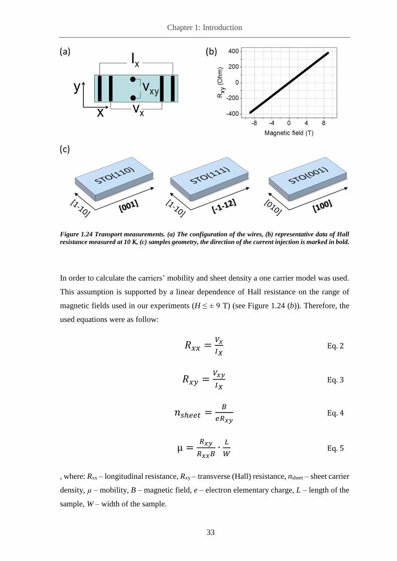
Chapter 1: Introduction
33
Figure 1.24 Transport measurements. (a) The configuration of the wires, (b) representative data of Hall
resistance measured at 10 K, (c) samples geometry, the direction of the current injection is marked in bold.
In order to calculate the carriers’ mobility and sheet density a one carrier model was used.
This assumption is supported by a linear dependence of Hall resistance on the range of
magnetic fields used in our experiments (H ≤ ± 9 T) (see Figure 1.24 (b)). Therefore, the
used equations were as follow:
𝑅𝑥𝑥 =𝑉𝑥
𝐼𝑋 Eq. 2
𝑅𝑥𝑦 =𝑉𝑥𝑦
𝐼𝑋 Eq. 3
𝑛𝑠ℎ𝑒𝑒𝑡 =𝐵
𝑒𝑅𝑥𝑦 Eq. 4
µ =𝑅𝑥𝑦
𝑅𝑥𝑥𝐵∙𝐿
𝑊 Eq. 5
, where: Rxx – longitudinal resistance, Rxy – transverse (Hall) resistance, nsheet – sheet carrier
density, µ – mobility, B – magnetic field, e – electron elementary charge, L – length of the
sample, W – width of the sample.

Chapter 1: Introduction
34
The transport measurements at low temperature were made in a Physical Property
Measurement System (PPMS) using the constant current mode of 1 µA. During a sweep
magnetic field was reaching a value of 9 Tesla in magnitude.
1.6.5. Ferroelectric characterization
The ferroelectric loops and leakage current were measured using a capacitor-like
configuration, having the investigated material in between the bottom electrode LNO and
the top electrode Pt. Platinum was chosen as material for the top electrode as it is a noble
metal (i.e. chemically resistive), easy to pattern (via a shadow mask or a lithography lift-
off), can be grown at room temperature and has a good rectifying characteristic [166]. After
cleaning the sample with acetone and ethanol, the Pt contacts were subsequently deposited
by means of magnetron sputtering using a grid as a shadow mask giving an array of contacts
about 60 µm by 60 µm in size, around 15 µm apart, and the thickness of about 20 nm. The
common used configurations for electric and ferroelectric tests are as called top-top (two
capacitors are measured in series) and top-bottom (a single capacitor is measured), see
Figure 1.25. In the top-bottom configuration the ground is connected to the bottom LNO
layer (using a silver paste), while the voltage is applied to a top Pt contact (using a W
needle16 controlled by a micropositioner17). On the other hand, in the top-top configuration,
both the ground and the voltage source are connected to two different top Pt contacts,
leading to the configuration of two capacitors connected in series by a LNO electrode which
now is floating (i.e. not grounded nor connected to a charge reservoir). Here the electric
field E is calculated as the applied voltage V divided by twice the distance between the
LNO and Pt electrodes. In this thesis, unless explicitly specified otherwise, all the electric
and ferroelectric measurements of BTO were performed in the top-top configuration. The
reason for this is that this configuration leads to a decrease of a leakage current for both
voltage polarities and lets to avoid asymmetric interface-related build-in electric
fields. [167,168]
16 The needle has a diameter of 20 µm, model SE-20TB, Signatone Co. http://www.signatone.com/ 17 Model S-725, Signatone Co.

Chapter 1: Introduction
35
Figure 1.25 The measurement configurations. (a) top-top and (b) bottom-top configurations and the
equivalent electric circuits.
The ferroelectric loops are recorded by applying a triangular voltage waveform and
measuring current using a virtual ground method18. Here, the basic equation for the
hysteresis measurements is:
𝑗(𝑉) = 𝑗l(V) + 𝑗tr(𝑉) +𝜕𝐷(𝑉)
𝜕𝑡 Eq. 6
, where: jl is the leakage current, jtr is the emission current from the traps existing in the
capacitor, D is the electric displacement, V is the applied voltage, t is time.
In turn, the electric displacement can be defined as:
𝐷 = 𝜀0𝐸 + 𝑃tot = 𝜀0𝐸 + 𝑃lin + 𝑃0 = 𝜀0𝐸 + 𝜀0𝜒𝐸 + 𝑃0 = 𝜀0𝜀r𝐸 + 𝑃0 Eq. 7
, where: E is the applied electric field, Plin is the linear polarization existing only when an
electric field is applied to the capacitor, P0 is the spontaneous polarization existing in the
ferroelectric, χ is the dielectric susceptibility, εr is the static dielectric constant. The term
ε0E is usually neglected in the case of ferroelectrics due to their χ ≫ 1; this will be also the
case in this thesis while referring to ferroelectric polarization (D ≡ Ptot).
18 For this we were using a ferroelectric tester TF2000 from aixACCT company http://www.aixacct.com/
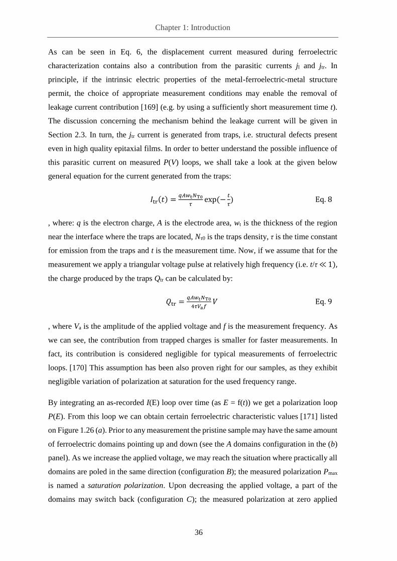
Chapter 1: Introduction
36
As can be seen in Eq. 6, the displacement current measured during ferroelectric
characterization contains also a contribution from the parasitic currents jl and jtr. In
principle, if the intrinsic electric properties of the metal-ferroelectric-metal structure
permit, the choice of appropriate measurement conditions may enable the removal of
leakage current contribution [169] (e.g. by using a sufficiently short measurement time t).
The discussion concerning the mechanism behind the leakage current will be given in
Section 2.3. In turn, the jtr current is generated from traps, i.e. structural defects present
even in high quality epitaxial films. In order to better understand the possible influence of
this parasitic current on measured P(V) loops, we shall take a look at the given below
general equation for the current generated from the traps:
𝐼tr(𝑡) =𝑞𝐴𝑤t𝑁T0
𝜏exp(−
𝑡
𝜏) Eq. 8
, where: q is the electron charge, A is the electrode area, wt is the thickness of the region
near the interface where the traps are located, Nτ0 is the traps density, τ is the time constant
for emission from the traps and t is the measurement time. Now, if we assume that for the
measurement we apply a triangular voltage pulse at relatively high frequency (i.e. t/τ ≪1),
the charge produced by the traps Qtr can be calculated by:
𝑄tr =𝑞𝐴𝑤t𝑁T0
4𝜏𝑉a𝑓𝑉 Eq. 9
, where Va is the amplitude of the applied voltage and f is the measurement frequency. As
we can see, the contribution from trapped charges is smaller for faster measurements. In
fact, its contribution is considered negligible for typical measurements of ferroelectric
loops. [170] This assumption has been also proven right for our samples, as they exhibit
negligible variation of polarization at saturation for the used frequency range.
By integrating an as-recorded I(E) loop over time (as E = f(t)) we get a polarization loop
P(E). From this loop we can obtain certain ferroelectric characteristic values [171] listed
on Figure 1.26 (a). Prior to any measurement the pristine sample may have the same amount
of ferroelectric domains pointing up and down (see the A domains configuration in the (b)
panel). As we increase the applied voltage, we may reach the situation where practically all
domains are poled in the same direction (configuration B); the measured polarization Pmax
is named a saturation polarization. Upon decreasing the applied voltage, a part of the
domains may switch back (configuration C); the measured polarization at zero applied

Chapter 1: Introduction
37
voltage Pr is named a remanent (remnant) polarization. Now, when we apply a voltage of
an opposite sense, we will eventually reach a point of null measured polarization
(configuration D); the corresponding electric field Ec is named a coercive field.
Figure 1.26 Poling and switching of the spontaneous polarization: (a) polarization versus electric field
hysteresis loop, (b) an example of possible corresponding domain structures (electrodes not shown). [171]
In the Dynamic Hysteresis Mode (DHM) the sample is exposed to four consecutive bipolar
voltage pulses in the sequence up-up-down-down (Figure 1.27 (a)). The used by us voltage
waveform was triangular, the delay time τ between the pulses equals 1 second and the
measurement frequency range between 1 kHz and 15 kHz (the value specified for each
measurement). The first and the third voltage pulse in DHM pre-polarize the sample to the
negative and positive state, respectively. Thanks to this the same measurement conditions
are met while recording the negative and positive part of the loop. The final hysteresis loop
is obtained by combining the current measured while applying a negative voltage (in the
second pulse) and a positive voltage (in the fourth pulse).
One way to remove the influence of parasitic leakage current from a ferroelectric
polarization loop is to perform the I(V) measurement in a Dynamic Leakage Current
Compensation (DLCC) mode. The DLCC voltage pulses sequence is based on two
consecutive DHM measurements, where the second one is done at the half of the

Chapter 1: Introduction
38
measurement frequency of the first one (see Figure 1.27 (b)). Here, the calculation of the
polarization is based on the assumption that the electric displacement is frequency
independent, while the amount of the electric charge resulting from the leakage current
depends on the measurement time. [172] All the ferroelectric loops presented in this thesis,
unless explicitly specified otherwise, were measured using the DLCC mode.
Leakage current is measured by applying a step shaped voltage waveform to the sample
and measuring the current by the virtual ground amplifier. Each voltage step lasts till the
current response becomes stable in the measurement time scale (for a few seconds) and
then the current integration time is in the range from 70% to 90% of the step time. The
leakage curves were obtained averaging I-V curves increasing and decreasing voltage.
1.6.6. Other techniques
The Pt top contacts were deposited by a sputtering. The sputtering process itself is defined
as the ejection of a material from a solid target due to the impact of energetic particles on
its surface. In the sputtering deposition the aforementioned target erosion is done by ion
bombardment of -in our case- argon, present in the chamber and ionized due to the applied
potential difference between the target and the substrate. In the RF (radio frequency)
variation of sputtering, this potential difference is varied at a typical frequency of 13.56
MHz. This enables formation of plasma, even for electrically insulating target materials. In
addition, in order to improve the yield of the sputtering process, a magnetron is used; the
created by it magnetic field allows a better confinement of the electrons close to the target.
At the beginning of the thesis a RF sputtering was used for the deposition of Pt contacts.
Later, it was replaced by a DC sputtering. The used by us RF sputtering deposition
Figure 1.27 A comparison between DHM (a) and DLLC (b) modes; ν0 is the measurement frequency and
τ is the delay time between pulses. [169]

Chapter 1: Introduction
39
parameters include: room temperature, an argon flux of 10 sccm, a power of 20 W and a
target-substrate distance of 6 cm. In turn, the DC sputtering was operating at the conditions
of: room temperature, an argon pressure of 5·10-3 mbar and a power 10 W, resulting in a
growth rate of 0.709 Å/s; in this case the chosen contact thickness was 20 nm. Prior to the
metallization, the samples were ultrasonically cleaned with acetone and ethanol.
Lattice parameters and epitaxial relationships were determined by X-ray diffraction (XRD)
using Cu Kα radiation. The θ-2θ symmetric scans and rocking curves were recorded using
a Siemens D500-2 circle diffractometer equipped with Ni-filters (eliminating the Kβ
contribution in the spectrum). In turn, for the pole figure and reciprocal space map
measurements the Bruker 1T8 Advance diffractometer equipped with a 2D detector was
used.
X-ray reflectivity (XRR) was one of the methods used in the thesis to define the thickness
of the thin films. This technique relies of the θ-2θ scans at very low angles (2θ between
0.5° and 6.0°) and the refractive effects, being relevant at these angles. The recorded
intensity versus angle plot features as called Kiessig fringes. The period of this oscillations
depends inversely on the film thickness. For the XRR measurements a Rigaku rotaflex RU-
200B was used.
Topographic images of the surfaces were recorded by atomic force microscopy (AFM) in
a dynamic mode in Keysight 5100 AFM or Keysight 5500 LS AFM setups. AFM is a
scanning probe technique sensitive to the forces interacting between a sharp tip and a
sample surface placed below. In the tapping mode, the cantilever with the probing tip
oscillates near it resonance frequency. When the tip is placed in a close distance from the
sample surface, the resulting force applied to the tip shifts it resonance frequency. While
scanning the sample, the change in the amplitude of the oscillations is corrected by
adjusting the tip-surface distance and thus the topographic image is recorded. In addition,
the phase difference between the driven sine wave and the cantilever response is also
recorded and yields the phase image. The phase image reflects the variations of the material
composition.
The pooled domains in BTO were observed using piezo force microscopy (PFM). PFM
works in a contact mode and the conductive tip acts as a top electrode. An alternating
voltage is applied causing deformations of the piezoelectric sample, and these periodic

Chapter 1: Introduction
40
surface vibrations are then transmitted back to the tip. As a result, there is a 180 ° phase
shift in the PFM response for the domains pointed up and down. In turn, for this collinear
polarization the PFM amplitude should be constant. In our case the measurements were
performed with a MFP-3D Asylum Research microscope. MikroMasch silicon cantilevers
with Pt coating (ANSCM-PT) were used. The dual AC resonance tracking (DART) method
was employed to achieve better sensitivity. [173]
Magnetization loops were measured in the 10 - 350 K range by superconducting quantum
interference device (SQUID) with the magnetic field applied in plane along Si[110].
Magnetization dependence on temperature has been measured using the same platform and
conditions after demagnetizing the sample to 5.5 µemu at low temperature. The used by us
SQUID was fabricated by Quantum Design.
Magnetic force microscopy (MFM) measurements have been performed using the same
AFM platform as in the PFM measurements. In MFM measurements the phase shift near
the cantilever resonance is tracked while keeping the cantilever at a constant distance (35
nm) from the surface. The cantilever (model MFM Hc from NT-MDT) had been
magnetized with a magnet before imaging.

41
Chapter 2 Ferroelectric BaTiO3 on silicon
Part of the work discussed in this chapter was later published in:
M. Scigaj, N. Dix, I. Fina, R. Bachelet, B. Warot-Fonrose, J. Fontcuberta, and F. Sánchez.
“Ultra-flat BaTiO3 epitaxial films on Si(001) with large out-of-plane polarization” Applied
Physics Letters 102, 112905 (2013).

Chapter 2 Ferroelectric BaTiO3 on silicon
42
Abstract
Monolithic integration of epitaxial c-oriented ferroelectric BaTiO3
with silicon constitutes a challenge as the functional layer usually
grows polycrystalline with high roughness or has low polarization.
Herein we have used a buffer layer heterostructure to achieve
epitaxial growth of c-oriented BaTiO3 onto silicon. The buffer
layers are grown on as-received Si(001) substrate and comprise of
Y:ZrO2, CeO2 and LaNiO3. The resulting BaTiO3 films have the
surface roughness of a few Å and feature ferroelectric remanent
polarization of 6-10 µC/cm2.

Chapter 2 Ferroelectric BaTiO3 on silicon
43
Monolithic integration of ferroelectric BTO on silicon is interesting from the point of view
of microelectronics. Despite large body of publications addressing the growth difficulties,
achieving epitaxial growth of high quality BTO on silicon was remaining elusive. Below
we present a structural and ferroelectric characterization of our state-of-art samples.
2.1. Growth of BaTiO3
BTO films were grown on Si(001) substrates using the YSZ/CeO2/LNO buffer structure.
The choice of the buffers and the related growth mechanisms are detailed in the Section
1.3.2. The used buffer layers thickness was: tLNO = 35 nm, tCeO2 = 20 nm and tYSZ = 35 nm.
Deposition conditions for the ferroelectric BTO itself include: substrate temperature T =
700 °C, laser repetition rate f = 5 Hz, oxygen partial pressure of PO2 = 0.02 mbar and
substrate-target distance of 46 mm. The deposition conditions are summarized in Table 2.
Table 2 The deposition conditions for the BTO/LNO/CeO2/YSZ/Si(001) samples.
After the growth the sample was cooled down in higher oxygen pressure of PO2 = 0.2 mbar.
This procedure was followed while growing the samples in the BTO thickness range of
nominally 19-825 nm.
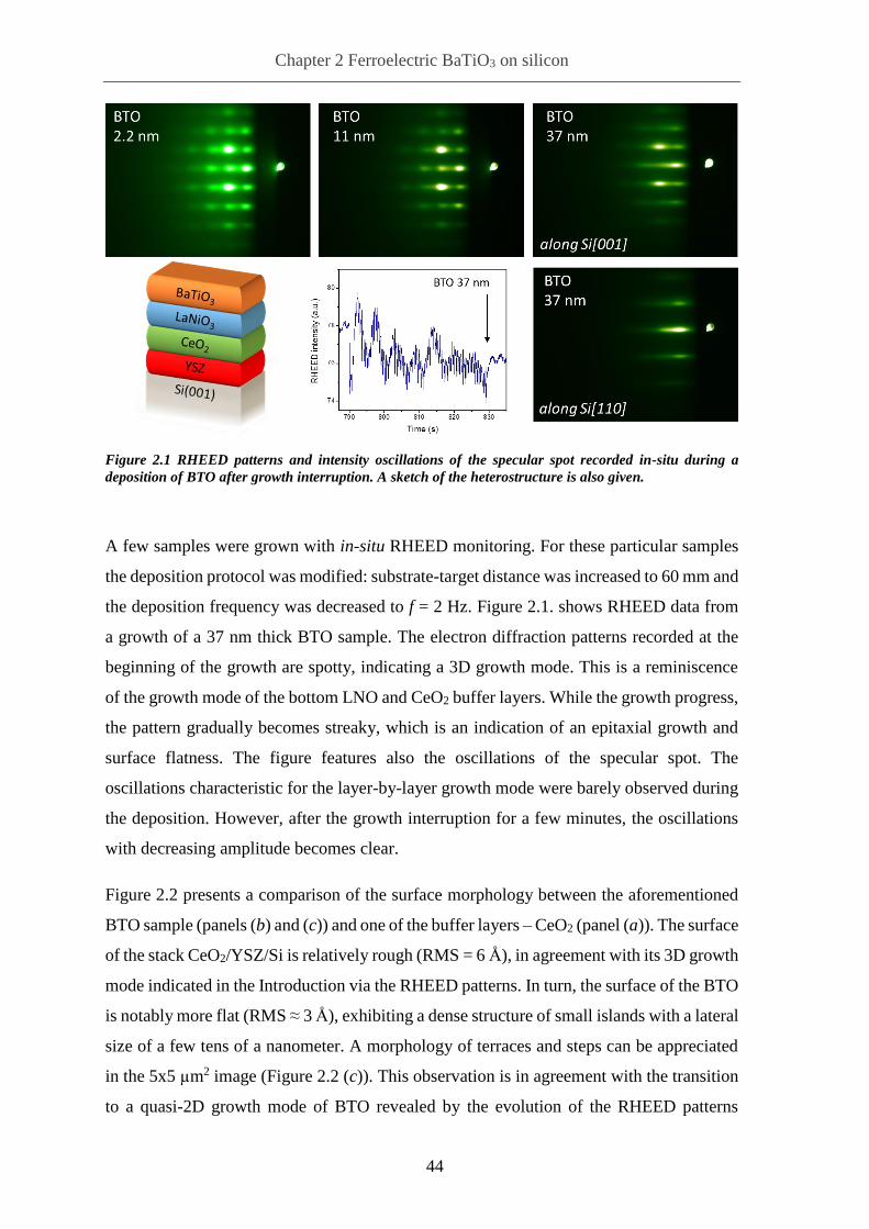
Chapter 2 Ferroelectric BaTiO3 on silicon
44
A few samples were grown with in-situ RHEED monitoring. For these particular samples
the deposition protocol was modified: substrate-target distance was increased to 60 mm and
the deposition frequency was decreased to f = 2 Hz. Figure 2.1. shows RHEED data from
a growth of a 37 nm thick BTO sample. The electron diffraction patterns recorded at the
beginning of the growth are spotty, indicating a 3D growth mode. This is a reminiscence
of the growth mode of the bottom LNO and CeO2 buffer layers. While the growth progress,
the pattern gradually becomes streaky, which is an indication of an epitaxial growth and
surface flatness. The figure features also the oscillations of the specular spot. The
oscillations characteristic for the layer-by-layer growth mode were barely observed during
the deposition. However, after the growth interruption for a few minutes, the oscillations
with decreasing amplitude becomes clear.
Figure 2.2 presents a comparison of the surface morphology between the aforementioned
BTO sample (panels (b) and (c)) and one of the buffer layers – CeO2 (panel (a)). The surface
of the stack CeO2/YSZ/Si is relatively rough (RMS = 6 Å), in agreement with its 3D growth
mode indicated in the Introduction via the RHEED patterns. In turn, the surface of the BTO
is notably more flat (RMS ≈ 3 Å), exhibiting a dense structure of small islands with a lateral
size of a few tens of a nanometer. A morphology of terraces and steps can be appreciated
in the 5x5 µm2 image (Figure 2.2 (c)). This observation is in agreement with the transition
to a quasi-2D growth mode of BTO revealed by the evolution of the RHEED patterns
Figure 2.1 RHEED patterns and intensity oscillations of the specular spot recorded in-situ during a
deposition of BTO after growth interruption. A sketch of the heterostructure is also given.

Chapter 2 Ferroelectric BaTiO3 on silicon
45
during the growth. Although terraces are not observed in most of the samples, even the 825
nm thick BTO film has a remarkably low roughness of about 9 Å. For the sake of
comparison, a morphology similar to the one of the BTO on silicon in Figure 2.2 was also
observed in much thinner (~5 nm thick) BTO films grown on the perovskite substrate
Nd:SrTiO3(001), where scanning tunneling microscopy confirmed they are multilayered
islands. [174]
2.2. Structural studies
A typical θ/2θ scan around symmetrical reflections of a BTO sample is given in Figure 2.3.
The strongest intensity peak on the left panel corresponds to the substrate Si(004). All other
Figure 2.2 A comparison of the surface morphology of the CeO2 buffer layer (a) and the BTO layer (b, c).
Figure 2.3 XRD θ-2θ scan of a sample with the BTO thickness of 220 nm. The zoomed area shows the data
coming from the samples with different BTO thickness; positions of the bulk BTO(002) and BTO(200)
reflections are also marked.

Chapter 2 Ferroelectric BaTiO3 on silicon
46
peaks belong to the 00l family of planes of the constituting layers: BTO, LNO, CeO2 and
YSZ. The right panel shows a magnification around the BTO(002) reflection. Here the
dashed lines mark the nominal position of the (002) and (200) reflections in the bulk, thus
corresponding to relaxed BTO with the c-axis being oriented out-of-plane and in-plane,
respectively. We can readily see that BTO in our structure is c-oriented and presenting
elongated c-axis parameter. Also it can be inferred from the right panel, that the BTO film
lowers its c-parameter as the thickness increases and at the thickness of 825 nm is already
fully relaxed. In addition, for the thickest 825 nm BTO film, a minor peak coming from the
(111)-oriented BTO appears. Here the XRD intensity ratio IBTO(111)/IBTO(001) is equal only
around 0.022% of the bulk values (not that in the plot the XRD intensity is given in a
logarithmic scale).
All BTO films grown (the thickness range 19-825 nm) are c-oriented (see Figure 2.4 (a)).
A progressive film relaxation is visible, from cBTO = 4.103 Å (19 nm) to from cBTO = 4.039
Å (825 nm). The sample corresponding to the blue triangle on the graph was cooled down
with a much higher oxygen pressure than standard samples (PO2 = 200 mbar instead of 0.2
mbar). The point fits in the trend with cBTO = 4.076 Å, thus showing that the presence of
oxygen vacancies is not the reason for the enlarged c parameter. In addition, the right panel
in the Figure 2.4 shows the lowering of the full width at half maximum (FWHM) of the
rocking curves around the BTO(002) reflection. The reduction of mosaicity with thickness
is not unexpected for the observed by us transition from 3D to 2D growth shown by the
evolution of the RHEED patterns.
Figure 2.4 (a) The out-of-plane lattice parameter of BTO plotted as a function of the film thickness; the
sample marked in blue was cooled down under high oxygen pressure (200 mbar). (b) A log-log plot of the
FWHM of the rocking curves of the BTO(002) reflection as a function of thickness; the inset shows
rocking curves of some of the samples.

Chapter 2 Ferroelectric BaTiO3 on silicon
47
The epitaxial relationship between the substrate and the deposited films was investigated
by means of XRD pole figures around asymmetrical reflections, recorded using a two-
dimensional (2D) detector. Representative frames at φ angle (respect to the Si[110]
direction) of 0° and 45° are given in the Figure 2.5 (a) and (b). The intensity integrated in
χ is plotted below the corresponding frames. At φ = 0° the Bragg spots correspond to h0l
family of planes of LNO and BTO, and to 111 planes of YSZ, CeO2 and Si (the last two
are overlapped). In turn, for the φ = 45° frame, 11l reflections of LNO and BTO and
202 reflections of YSZ, CeO2 and Si are observed. This implies that YSZ and CeO2 grow
cube-on-cube on Si, while LNO and BTO are rotated 45° in-plane, as expected from the
lattice mismatch.
Figure 2.5 XRD measurements, of a sample with a 55 nm thick BTO layer, acquired by means of a 2D
detector. 2θ-χ detector frames around in-plane sample directions (with respect to Si[110]) of ϕ = 0o(a) and
ϕ =45o(b), with the corresponding integrated intensity along χ plotted below.
The same epitaxial relationship is readily visible from the pole figures recorded around
101 reflections of Si and films, depicted in Figure 2.6. Therefore, the epitaxial
relationship can be in short written as [110]BTO(001) || [110]LNO(001) || [100]CeO2(001)
|| [100]Si(001). A corresponding simplified sketch is shown in the right panel.

Chapter 2 Ferroelectric BaTiO3 on silicon
48
Figure 2.6 Pole figures, of the sample with t(BTO) ≈ 55 nm, around given reflections of the sample’s
constituting materials (left). On the right, a schematic cartoon of the heterostructure showing the epitaxial
relationships.
In order to get a better insight on the films and interfaces structural quality a TEM study
has been performed on a sample with tBTO ≈ 50 nm. The whole multilayer stacking is visible
in the low magnification cross-section TEM image in Figure 2.7 (a). Here one can
appreciate the smooth BTO surface and the perfectly resolved interfaces. The last point is
confirmed by the series of high resolution images in panels (b-e). In addition, the YSZ/Si
interface features an interfacial SiOx layer with the thickness of about 3 nm, while the
overlaying YSZ layer presents excellent crystalline order and sharp interface with CeO2.
The high contrast within the LNO and BTO layers suggests thickness fluctuations of the
TEM specimen, thus limiting the possibility of identification of defects.

Chapter 2 Ferroelectric BaTiO3 on silicon
49
Figure 2.7 TEM cross-section characterization of a sample with ≈ 50 nm thick BTO. On the left, a low
resolution image showing the whole stack. The remaining images display the particular interfaces in a
high resolution.
2.3. Electric and ferroelectric properties
The main purpose of this Chapter is to present a monolithic integration of ferroelectric BTO
on silicon. In this Section we present the electrical and ferroelectric properties of our
structures. The ferroelectric characterization of the BTO-based samples was done by
measuring current (I) versus applied electric field (E), as explained in the Introduction. A
representative I(E) curve of a sample with 55 nm thick BTO is given in the inset of Figure
2.8 (a), showing ferroelectric switching peaks at about 300 kV/cm. Polarization (P) loops
were obtained by integrating current over time. The corresponding loop presented in panel
(a) indicates the remanent polarization (Pr) and saturation polarization (Ps) of around 10
µC/cm2 and 20 µC/cm2, respectively. Polarization loops of thicker samples (tBTO = 138 and
440 nm) are also shown. The corresponding Pr are respectively around 7 and 4 µC/cm2. As
can be seen in the Figure 2.8 (b), most of the deposited samples are characterized by the
remanent polarization laying in the range 6-8 µC/cm2, however the direct dependence on

Chapter 2 Ferroelectric BaTiO3 on silicon
50
thickness cannot be readily appreciated from the plot. It is usually observed that Pr scales
with the tetragonality of the ferroelectric film. In our case we can see that the measured
remanent polarization scales the BTO c lattice parameter (Figure 2.8 (c)). Moreover, it can
be appreciated that the ferroelectric loops in the panel (a) largely differ in the coercive field
(Ec). The log-log plot of the Ec versus the BTO thickness is shown in the (d) panel. The
dashed line in the plot indicates the common scaling for ferroelectric thin films
Ec ∝ t -2/3 [175]. The experimental data match pretty well to this model, while a linear fit
(not shown here) gives a similar power coefficient of -0.73(9). The data corresponding to
the thickest 825 nm BTO sample are not shown in the figure, as the voltage available in the
measurement station was not sufficient to saturate the sample.
Figure 2.8 Polarization loops of the samples with different BTO thickness (a); the inset presents the
current-voltage loop of the sample with t(BTO) = 55 nm. Remnant polarization plotted as a function of the
BTO thickness (b) and the BTO out-of-plane parameter (c). Coercive field plotted versus the BTO thickness
(d); the dashed line is a linear fit with the slope of -⅔.

Chapter 2 Ferroelectric BaTiO3 on silicon
51
Figure 2.9 Leakage current of a sample with 55 nm BTO (a), J-E linear relationship for the SCLC
mechanism (b) and the modified Schottky mechanism (c); α coefficient is taken from log J = α · log E; Ne
is the effective charge density at the interface. The vertical bar in panels (b) and (c) indicate the apparent
transition between 23.2 kV/cm2 and 47.4 kV/cm2.
Leakage current can be a problem in a capacitor. A representative leakage curve of a 55 nm
thick BTO sample is depicted in Figure 2.9 (a). The presented resistance characteristic is
comparable to other ferroelectric thin films on silicon, e.g. PZT [43] and BiFeO3 [176]
single layers and PZT/spinel [177] bilayers.
If the leakage current is bulk limited by means of Space Charge Limited Conduction
(SCLC), the leakage current density follows the relation:
log 𝐽 ∝ α log 𝐸 Eq. 10
, where J is the current density, E is the electric field and α is a factor further defines the
conduction limiting factor. The α = 1 describes the Ohm’s law region, while α = 2 can be
attributed to both the traps-filled limit current or the Child’s law. [178] When we plot the

Chapter 2 Ferroelectric BaTiO3 on silicon
52
experimental data according to the equationlog 𝐽 ∝ α log 𝐸 Eq. 10 we obtain a straight line
with the slope α = 1.19 for fields below 23.2 kV/cm2 (Figure 2.9 (b), here only a
representative plot for the positive voltage side is shown). This means that the SCLC
mechanism cannot be ruled out here.
In turn, for electric fields above 47.4 kV/cm2 the leakage current fits well in the interface-
limited modified Schottky emission model. The Schottky emission is a common
phenomenon in ferroelectric oxides being in contacts with metallic electrodes. Due to the
presence of polarization charge, ferroelectrics required more complex approach than
classical semiconductors. Following the physical model described in ref. [167], for the
modified Schottky emission current density follows the equation:
ln 𝐽 = 𝑏(𝑉 + 𝑉𝑏𝑖)14⁄ Eq. 11
𝑏 =𝑞
𝑘𝑇√
𝑞3𝑁e
8𝜋2𝜀d2𝜀𝑠𝜀0
3
4 Eq. 12
, where J – current density, V – applied voltage, Vbi – build-in potential, q – electronic
charge, k – Boltzmann constant, T – temperature, Ne – effective charge density in the
depletion layer, εd – dynamic electric constant, εs – static electric constant, ε0 – vacuum
permittivity.
The data for fields above 47.4 kV/cm2 fit well with this model (Figure 2.9 (c)). Assuming
εs = 264 [179] and εd = 17 [180], the effective charge density has been estimated to be of
the order of Ne = 1021 cm-3. This is a comparable value for the Pt/BTO and BTO/LNO
interface reported in literature. [167,179] This value is important, as space charges have a
significant influence on the electrical properties of ferroelectric structures (like e.g. the size
and shape of the ferroelectric hysteresis loop). [181]
Despite the fact that the experimental data fit very well to the theoretical models, more
extended studies are required in order to fully understand the physical processes underlying
the full leakage characteristic. Further research may include measuring the influence of
temperature [182] and relaxation time [183] on the leakage current.

Chapter 2 Ferroelectric BaTiO3 on silicon
53
2.4. Conclusions
In this Section we showed epitaxial integration of ferroelectric BTO films on a Si(001)
substrate. This was obtained using the buffer structure of LNO, CeO2 and YSZ. The
resulting BTO films are very flat and have a remanent polarization up to 10 µC/cm2. This
result is remarkable especially as the total thickness of the buffer layers is below 100 nm.
We consider the reported herein growth protocol as an important step in the integration of
BTO in monolithic devices of silicon. In particular, by using our structure as a platform for
growth of CoFe2O4 we could obtain a room temperature multiferroic on silicon, the results
discussed further in the following Section.


55
Chapter 3 CoFe2O4/BaTiO3 on silicon
Part of the work discussed in this chapter was later published in:
M. Scigaj, N. Dix, J. Gázquez, M. Varela, I. Fina, N. Domingo, G. Herranz, V. Skumryev,
J. Fontcuberta, F. Sánchez “Monolithic integration of room-temperature multifunctional
BaTiO3-CoFe2O4 epitaxial heterostructures on Si(001)” Scientific Reports, 6, 31870 (2016)

Chapter 3 CoFe2O4/BaTiO3 on silicon
56
Abstract
Technologically desired room temperature multiferroic materials
are elusive in a single phase, however they can be achieved
combining two ferroic phases. Herein we report monolithic
integration on the silicon platform of the lead-free
CoFe2O4/BaTiO3 horizontal bilayer. The growth was accomplished
with the use of a LaNiO3/CeO2/YSZ tri-layer buffer system. Thus
obtained functional materials exhibit high structural quality, close
to those achieved on perovskite substrates. Robust ferromagnetism
and superior ferroelectric properties at room temperature are
obtained.

Chapter 3 CoFe2O4/BaTiO3 on silicon
57
The combination of two ferroic oxides as an artificial multiferroic system is an alternative
to single multiferroic materials for room temperature operation. [184] Regarding the form
of thin films, most of the research has been done using non technological substrates, mainly
perovskites. Using silicon substrates high quality epitaxial growth of vertical
nanocomposites formed by the FE perovskite BiFeO3 and the FM insulator spinel CoFe2O4
(CFO) has been reported [185]. Horizontal heterostructures with FE and FM
films [80,184,186] are more convenient than vertical nanostructures for device fabrication.
However, perovskites and spinels are highly dissimilar, which hinders epitaxial growth
when they are combined in horizontal heterostructures. This additional difficulty makes the
integration of epitaxial horizontal bilayers of multiferroic oxides with Si, with structural
and functional properties close to those of bilayers on perovskite substrates, extremely
challenging. Although epitaxial growth has been reported [187], multiferroic oxide thin
film bilayers on Si are generally polycrystalline and present high surface
roughness [177,188–190]. Most of the reported multiferroic bilayers include PbZrxTi1−xO3
(PZT) as FE oxide. However, Pb-free ferroelectrics are preferable, and the successful
epitaxial integration of BTO films on Si(001) shown in the previous Chapter paves the way
towards this goal. Thus, we have grown horizontal top-CFO/bottom-BTO heterostructures
on Si(001) buffered LNO/CeO2/YSZ. CFO is a ferrimagnetic oxide with high
magnetization above 400 emu/cm3 and Tc well above RT [75]. As we will show, the
CFO/BTO bilayers here reported display a combination of structural and functional
properties until now elusive in either Pb-free or PZT-based multiferroic bilayers
3.1. Growth of CoFe2O4
The bilayers CFO/BTO were grown on a Si(001) substrate buffered with LNO/CeO2/YSZ.
The details of the integration of BTO on Si are given in the previous Chapter. A series of
CFO/BTO samples were made with a varying thickness of the CFO capping layer, between
tCFO = 35-70 nm, while keeping the BTO thickness at nominally tBTO = 55 nm. The CFO
growth parameters include: temperature T = 500 °C, oxygen partial pressure PO2 = 0.1 mbar
and laser frequency f = 5 Hz.

Chapter 3 CoFe2O4/BaTiO3 on silicon
58
3.2. Structural characterization
X-ray diffraction in the θ-2θ scan geometry around symmetrical reflections of the sample
with the thickest CFO (tCFO = 70 nm) is shown in Figure 3.1 (a). Only peaks belonging to
the 00l family of planes of the deposited layers are visible indicating absence of other
film’s orientations and secondary phases. The zoomed area around the CFO(004),
BTO(002) and LNO(002) reflections is depicted in the panel (b), together with samples of
tCFO = 35 nm and 0 nm. We can see that the CFO(004) peak intensity increases along with
the film thickness. Regardless of the presence of the capping CFO layer, the BTO is c-
oriented with increased tetragonality; the out-of-plane lattice parameter is around 4.06 Å.
Figure 3.1 XRD data of the sample with tCFO = 70 nm. A θ-2θ scan around symmetrical reflections (a)
and a zoomed area (b) with indicated by the dashed lines the bulk BTO(002) and (200) reflections. (c) A
ϕ-scan around asymmetrical reflections coming from the constituting layers. On the bottom-right is
depicted a sketch of the heterostructure.
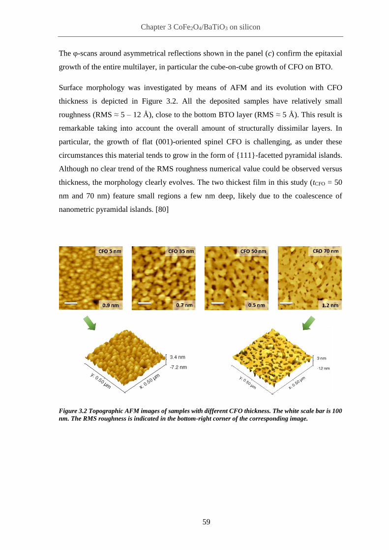
Chapter 3 CoFe2O4/BaTiO3 on silicon
59
The φ-scans around asymmetrical reflections shown in the panel (c) confirm the epitaxial
growth of the entire multilayer, in particular the cube-on-cube growth of CFO on BTO.
Surface morphology was investigated by means of AFM and its evolution with CFO
thickness is depicted in Figure 3.2. All the deposited samples have relatively small
roughness (RMS ≈ 5 – 12 Å), close to the bottom BTO layer (RMS ≈ 5 Å). This result is
remarkable taking into account the overall amount of structurally dissimilar layers. In
particular, the growth of flat (001)-oriented spinel CFO is challenging, as under these
circumstances this material tends to grow in the form of 111-facetted pyramidal islands.
Although no clear trend of the RMS roughness numerical value could be observed versus
thickness, the morphology clearly evolves. The two thickest film in this study (tCFO = 50
nm and 70 nm) feature small regions a few nm deep, likely due to the coalescence of
nanometric pyramidal islands. [80]
Figure 3.2 Topographic AFM images of samples with different CFO thickness. The white scale bar is 100
nm. The RMS roughness is indicated in the bottom-right corner of the corresponding image.

Chapter 3 CoFe2O4/BaTiO3 on silicon
60
The Figure 3.3 depicts cross-section images of a sample with tCFO = 50 nm, recorded19 in a
STEM mode using a HAADF detector. In the left panel we can see that each layer is of
uniform thickness over all the image lateral length. No secondary phases could be observed
within any layer neither at any of the interfaces. Between the Si substrate and the YSZ
buffer layer appears a few nm thick interfacial layer of SiOx (not visible at the low
magnification). Presented in the right panel high magnification image confirms the cube-
on-cube epitaxial relationship between the two functional layers; here a sharp interface is
apparent.
3.3. Electric and ferroelectric properties
Representative ferroelectric P(V) loops of a sample with 35 nm thick CFO layer and a
reference bare BTO sample are given in the Figure 3.4, in green and red respectively. The
corresponding current versus voltage I(V) loops are given in the insets. The I(V) loops show
clear ferroelectric switching peaks, with the resulting P(V) loops having textbook concave
regions [191]. The coercive voltage of the sample with CFO (≈ 7.5 V) is higher than in the
bare BTO films (≈ 3 V). This is in the perfect agreement with the picture of both CFO and
19 The images were recorded by dr. Jaume Gázquez, a scientist working at ICMAB, in collaboration with the
STEM Group of the Oak Ridge National Laboratory, USA (http://stem.ornl.gov/).
Figure 3.3 STEM high angle annular dark field imaging. On the left, low magnification image along the
Si[100] zone axis. On the right, a high resolution image of the interface between the perovskite BTO and
the spinel CFO along the BTO[110] zone axis.

Chapter 3 CoFe2O4/BaTiO3 on silicon
61
BTO being good insulators with dielectric constants of εCFO = 14 [192] and εBTO = 60 [193],
respectively. The right panel in the Figure 3.4 makes a comparison between the samples
with CFO (green squares) and with bare BTO discussed in the previous Chapter (the red
line). A high remanent polarization of about Pr = 20 µC/cm2 was measured for all five
investigated samples. Therefore, this crucial ferroelectric parameter has been increased by
a factor of ≈ 3 by the in-situ growth of CFO capping layer. The result is of high interest
also because the presence of insulating CFO does not result in the existence of depolarizing
field strong enough to preclude the establishment of a monodomain polar state along the
out-of-plane direction. Here the most probable scenario for the depolarizing field
compensation seems to rely on a migration of free charges from the bulk of BTO or CFO
to the interface. In turn, the observation of the high remanent polarization up to Pr ≈ 23
µC/cm2 for CFO/BTO samples, compared to about Pr ≈ 6-7 µC/cm2 for samples with bare
BTO, could originate from different electrical boundary conditions of the two systems
while cooling down below the Currie temperature after the deposition. In particular, the
bare BTO is exposed to vacuum leading to the highest depolarization field. [194] This in
turn should result in the presence of compensating domains which degrade the switchability
(via pinning of the ferroelectric domains) and favor low retention (via creation of stray
fields). In contrary, CFO could provide free charges largely compensating the depolarizing
field.
Figure 3.4 On the left, polarization-voltage loops of the sample tCFO = 35 nm (in green) and of a sample
without any CFO overlayer, both having the same thickness of BTO; the corresponding current-voltage
plots are shown in the top-left and bottom-right insets respectively. On the right, the remnant polarization
as a function of the CFO thickness measured at 4 kHz; the vertical bar at tCFO = 0 nm indicates the range
of polarization values measured for the analogous films without the CFO layer, discussed in the previous
Chapter.

Chapter 3 CoFe2O4/BaTiO3 on silicon
62
As it was described in the Introduction, the I(V) loops are measured in the DLCC variation
of the standard DHM mode. Figure 3.5 shows the advantageous effect of using the DLCC
mode on the samples as presented in the left panel of Figure 3.4. Here we can see, that in
the both samples the DLCC only compensates the leakage contribution without producing
a significant change in the position nor the amplitude of the ferroelectric switching peaks.
Only in the case of the CFO/BTO sample a slight change in the peak shape can be observed.
This is due to larger variation of the coercive field with the measurement frequency for this
set of samples.
Figure 3.5 The comparison between DHM-only and DLCC measurements. The corresponding I-V loops
for samples with and without CFO top layer are shown.
The Figure 3.6 presents a comparison of leakage current density between two samples: one
with 50 nm CFO and 55 nm BTO (in green), the other with 110 nm of bare BTO (in red).
Note that the total nominal thickness of the functional layers between the LNO and Pt
electrodes is almost the same. It is seen that, substituting a part of the BTO layer with a
CFO layer results in lowering the leakage. Here a decrease of about one order of magnitude
is observed. For instance, applying a voltage of 2 V results in a leakage current density of
around 5·10-5 A/cm2 for the sample without CFO, but only 5·10-6 A/cm2 for the CFO/BTO
bilayer. This value is much lower or at least comparable to results obtained on thicker
ferroelectric PZT [43] and BiFeO3 [176] single layers and PZT/spinel bilayers [177] on
Si(001). Qualitatively similar drop in the leakage current density was observed for

Chapter 3 CoFe2O4/BaTiO3 on silicon
63
CFO/PZT bilayers grown on STO, however it was accompanied by a drop in both remanent
and saturation polarization. [195] This discrepancy could be explained by the used growth
temperature being lower than the real Currie temperature of PZT in this structure.
Figure 3.6 Leakage current density versus voltage; the data corresponds to the bare BTO sample with tBTO
= 110 nm (in red) and to the sample with tBTO = 55 nm and tCFO = 50 nm (in green). The inset shows the
same set of data in the log-log scale, thus providing a better comparison for leakage at lower voltage.
One of the challenges of current and future memory devices based on ferroelectric materials
is fatigue. In this case fatigue is understand as hindering of ferroelectric properties upon
cycling a sample in an electric field which switches the polarization of the functional layer.
It is well known, that the choice of electrodes has a significant influence of the electric and
ferroelectric properties of a thin layer. In particular, metallic electrodes generally have
better leakage rectifying characteristic than oxide electrodes [182,196], while the later
enables better fatigue endurance [197]. Herein we use an oxide CFO layer, which in this
case acts as a buffer layer between BTO and Pt.
Fatigue depends on factors such as temperature, cycling voltage amplitude, frequency and
waveform. Therefore, we performed our benchmarking in a well-controlled environment
using cycling conditions possibly close to the ones used in industry (within the limitations
of our measurement setup). During the test a sample was placed on a dissipating heat metal
radiator. Applied voltage waveform was the square one with the amplitude of ± 10 V and
frequency of 100 kHz. The fatigue test was exceptionally done in the top-bottom
configuration, as it is electronically closer to the one employed in commercial FeRAMs.
-4 -2 0 2 410
-9
10-8
10-7
10-6
10-5
10-4
Curr
ent
density (
A/c
m2 )
Voltage (V)
BTO
CFO/BTO
0.1 1 10
1E-7
1E-6
1E-5
1E-4
1E-3

Chapter 3 CoFe2O4/BaTiO3 on silicon
64
The ferroelectric loops were measured ten times per a cycling decade with the standard
DLCC mode, a voltage amplitude of ± 10 V and a frequency of 4 kHz. The representative
results are shown in Figure 3.7; here the sample contains 50 nm think CFO layer. We can
readily see that CFO/BTO bilayer exhibits excellent endurance against ferroelectric fatigue.
The measurement was stopped at 5·10-10 cycles, which seems to represent virtually
unlimited cyclability for most of the applications of FeRAM. During the entire test the
sample kept the high remanent polarization of about 22 µC/cm2 with the ferroelectric loop
showing no remarkable difference. The used by us number of fatigue cycles is approaching
the cyclability warranty limit of commercially available Pb-based Fujitsu FeRAMs (1012
cycles 20). We could not check this upper limit as the required test, at the used by us cycling
conditions, would take about 4 months.
Figure 3.7 On the left, a remanent polarization as a function of the number of voltage sweep cycles for a
sample with tCFO = 50 nm. On the right, polarization versus voltage loops of the same sample in the
pristine state (just before cycling) and just after 5x10¹⁰ cycles.
In order to confirm the actual ferroelectric switching we performed additional
measurement. Figure 3.8 (a) shows ferroelectric loops at increasing voltage amplitude for
the same sample which fatigue properties were discussed above. Here the measurement
conditions (namely a triangular voltage waveform, a frequency of 4 kHz and the DLCC
mode) result in fairly saturated loop at 10 V with the saturation polarization of about Ps ≈
20 Source: Fujitsu FeRAM overview

Chapter 3 CoFe2O4/BaTiO3 on silicon
65
39 µC/cm2. The (b) panel shows current and polarization versus time for the exact
conditions as used for cycling (namely voltage 10 V, high frequency 100 kHz and the
square voltage waveform). Here the resulting saturation polarization Ps ≈ 37 µC/cm2 is
almost the same as in the case of a standard measurement, thus one can conclude that the
ferroelectric switching occurred during each cycle. The last graph in panel (c) shows a
result of applying a square voltage waveform at 4 kHz and 10 V (so the same as in panel
(a)), resulting in Ps ≈ 44.5 µC/cm2; the excess of the calculated charge could result for
instance from leakage and further saturation of the BTO. This further confirms that the
sample was being fully switched upon cycling.
Figure 3.8 Data of the sample with CFO 50 nm on BTO 55 nm. (a) P-V loops recorded with a triangular
voltage waveform, at 4 kHz with DLCC. Measured current and integrated polarization as a function of
time upon application of a square volatage waveform with 10 V amplitude at 100 kHz (b) and 4 kHz (c).

Chapter 3 CoFe2O4/BaTiO3 on silicon
66
The piezoelectric properties of the bilayers were investigated by means of piezoresponse
force microscopy (PFM). PFM voltage hysteresis loops were always performed at
remanence, using a dwell time of 100 ms. A representative set of data from measurements
of a sample with 50 nm CFO is given in Figure 3.9. The (a) and (b) panels feature typical
PFM hysteresis loops, where phase and amplitude (proportional to the d33 piezoelectric
coefficient) are changing upon cycling voltage. The 180 ° phase shift in the panel (a) signals
the piezoelectric nature of the heterostructure. We can also notice that the loop is shifted
towards negative values of voltage, which indicate the presence of a significant imprint
field corresponding to an electric field towards the bottom LNO electrode. This means that
the polarization in as-grown sample is pointing down (Pdown). The imprint field most
probably originates from the difference in work functions of the top (Pt) and bottom (LNO)
electrodes along with the general asymmetry of the CFO/BTO structure. In the panel (b) is
shown the corresponding ferroelectric butterfly loop for the amplitude response. Here the
imprint is also visible and results in the existence of bi-stable strain states at zero applied
Figure 3.9 PFM characterization. Piezoresponse phase (a) and amplitude (b) versus applied voltage loops,
recorded with an AC driving voltage Vac = 1 V. Images of piezoresponse phase (c) and amplitude (d)
measured with Vac = 1 V, after poling the areas with +6 V and -6 V; the scale bar indicates 4 µm.

Chapter 3 CoFe2O4/BaTiO3 on silicon
67
voltage. As can be seen from the amplitude and phase response, the Pdown (and as-grown)
state corresponds to a strain state of more elongated out-of-plane parameter, compared to
the Pup polarization state. The coercive voltage inferred from the both panels (a) and (b)
(~3 V) corresponds well with the coercive voltage of the same sample measured in P(V)
loops (Figure 3.8 (a)). The capability of writing up and down ferroelectric domains by
means of AFM tip induced electric field was summarized in Figure 3.9 panels (c) and (d).
The (c) panel presents the phase image after poling the sample with +6 V (dark areas) and
-6 V (bright areas). The contrast of the piezoresponse signal is nearly 180°. The
corresponding piezoresponse amplitude image is given in the panel (d). Note that here the
contrast originates from the two remanent values of amplitude resulting from the existence
of the aforementioned imprint field.
3.4. Magnetic properties
In the previous Section we saw the influence of CFO on the electrical, piezo- and
ferroelectric properties of the heterostructure. Here we will take a fast look at the magnetic
properties of the CFO. The investigated sample has 70 nm thick CFO layer. Magnetization
loops were measured at various temperatures in the 10 K - 350 K range with the field
applied along the CFO[100] in-plane direction. The loops measured at 10 K and 300 K are
depicted in Figure 3.10 (left panel). The visible in the M(H) loops double step is a common
experimental observation in spinel oxides [198–203] and other ferrimagnetic oxides like ε-
Fe2O3 [204] as well as ceramic samples [205]. The saturation magnetization of about Ms ≈
250 emu/cm3 at 10 K is lower than the value of bulk CFO, as commonly observed of this
films deposited on perovskite surfaces. [198–201] In the right panel of Figure 3.10 we can
see that Ms decreases slightly with temperature and remains above 200 emu/cm3 up to 350
K. From this we can infer that the Curie temperature is well above the room temperature as
in the bulk material. [206] In turn the coercive field Hc decreases from about 1.0 T at 10 K
to 0.1 T at 350 K, which indicates the change in the magnetic anisotropy. The ratio of the
remanent magnetization to the saturation magnetization is equal about 0.46 at 10 K and
0.17 at room temperature.

Chapter 3 CoFe2O4/BaTiO3 on silicon
68
Figure 3.10 (a) Magnetization loops of the sample with tCFO = 70 nm measured at 10 K and 300 K with the
field applied in-plane along Si[110]. (b) The temperature dependence of the magnetization (left axis) and
the coercive field (right axis).
3.5. Magnetoelectric characterization
In the previous Sections we took a look at the ferroelectric and magnetic properties of the
functional layers in the samples. The fact that these two materials were grown in the same
heterostructure could permit magnetoelectric coupling. The used by us magnetic material
is nominally insulating and thus the electric field effect originating from the polarization
acting upon the CFO can be neglected. Therefore, only the direct coupling based on the
elastic interaction between the two layers should be considered. On the other hand, in
epitaxial heterostructures, the elastic interactions between two active films is hindered by
a strong clamping of the substrate. In this case, the magnetoelectric coupling largely
depends on the materials and their structure. [207] In fact, a strong dependence between
the magnetoelectric coupling and factors like the crystal orientation, relative buffer
thickness, the buffer layer material and the direction of the applied magnetic field has been
reported for CFO/BTO and CFO/PZT bilayers. [208–210] The measured magnetoelectric
coefficients were ranging from negligible up to about 100 mV/cm·Oe.
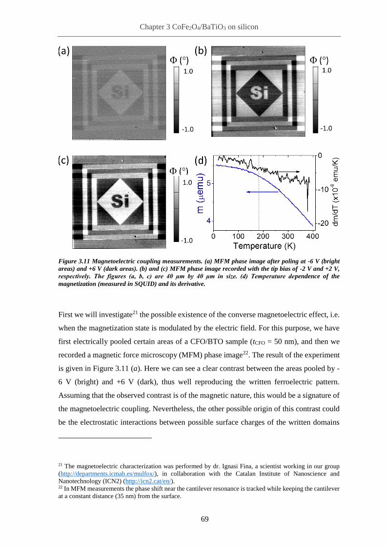
Chapter 3 CoFe2O4/BaTiO3 on silicon
69
First we will investigate21 the possible existence of the converse magnetoelectric effect, i.e.
when the magnetization state is modulated by the electric field. For this purpose, we have
first electrically pooled certain areas of a CFO/BTO sample (tCFO = 50 nm), and then we
recorded a magnetic force microscopy (MFM) phase image22. The result of the experiment
is given in Figure 3.11 (a). Here we can see a clear contrast between the areas pooled by -
6 V (bright) and +6 V (dark), thus well reproducing the written ferroelectric pattern.
Assuming that the observed contrast is of the magnetic nature, this would be a signature of
the magnetoelectric coupling. Nevertheless, the other possible origin of this contrast could
be the electrostatic interactions between possible surface charges of the written domains
21 The magnetoelectric characterization was performed by dr. Ignasi Fina, a scientist working in our group
(http://departments.icmab.es/mulfox/), in collaboration with the Catalan Institute of Nanoscience and
Nanotechnology (ICN2) (http://icn2.cat/en/). 22 In MFM measurements the phase shift near the cantilever resonance is tracked while keeping the cantilever
at a constant distance (35 nm) from the surface.
Figure 3.11 Magnetoelectric coupling measurements. (a) MFM phase image after poling at -6 V (bright
areas) and +6 V (dark areas). (b) and (c) MFM phase image recorded with the tip bias of -2 V and +2 V,
respectively. The figures (a, b, c) are 40 µm by 40 µm in size. (d) Temperature dependence of the
magnetization (measured in SQUID) and its derivative.

Chapter 3 CoFe2O4/BaTiO3 on silicon
70
and the magnetic and metallic MFM scanning tip. In order to discriminate between these
two scenarios, additional MFM imaging was done with the magnetic tip bias of -2 V and
+2 V. The images are shown in the panels (b) and (c) respectively. The contrast
enhancement in the (c) panel and the contrast reversal in the (b) panel revel that the
observed contrast is dominated by electrostatic charges, and thus the magnetoelectric effect,
if any, remains imperceptible. In other experiment, we have investigated the existence of
the direct magnetoelectric coupling by measuring the ferroelectric loops under a magnetic
field of 1 T applied in-plane. No meaningful change was observed.
In addition, an indirect method was used to check the possible existence of a converse
magnetoelectric coupling. As it was shown in the Introduction, BTO undergoes several
structural changes at certain temperatures. During these transitions domains structure and
a position of the polarization axis are changing. This transformation should have an effect
on the properties of the overlaying magnetic CFO layer, as it was observed in CFO film
grown on BTO crystals [211]. In order to investigate the existence of this effect in our
samples we have measured in SQUID at the magnetic field of H = 30 Oe applied in-plane
the change in magnetization while varying the temperature. The resulting magnetization
and it’s derivative over the temperature are plotted in Figure 3.11 (d). The dashed lines
correspond to the bulk BTO phase transitions. However, no anomalies were observed. This
might be due to the clamping between the thick silicon substrate and the epitaxially grown
BTO thin film, as it has been reported that this effect can largely alter the BTO phase
transitions. [212]
At first, these results may seem to contradict with the reported large magnetoelectric
coupling of about 100 mV/cm·Oe in CFO/BTO bilayers on perovskite substrates. [210]
However we stress, that these measurements were done with a time dependent Hac field
superimposed on Hdc while electromotive force is recorded. Therefore, the dynamic
magnetoelectric coupling reported in references [208–210] is different than the determined
by us static quasi-equilibrium response. Future studies will be devoted to understand the
microscopic mechanism leading to these different responses and consequently to different
magnetoelectric coupling coefficients.

Chapter 3 CoFe2O4/BaTiO3 on silicon
71
3.6. Conclusions
The CFO/BTO bilayer was monolithically integrated on a Si(001) substrate with the use of
LNO/CeO2/YSZ buffer layers. All the layers grow epitaxially resulting in a flat surface.
The BTO is c-oriented with extended the out-of-plane parameter. The samples show
multifunctional properties at room temperature, namely a high magnetization and excellent
ferroelectric properties.
We note that our research can be of high interest for certain memory devices, like e.g. the
non-volatile four states multiferroic monolithic memories. FE-field effect transistors (FE-
FETs) constitute another example. [11] In this case the functional limitations origin from a
low retention time and endurance. Here we show that the use of a proper insulating layer
may lower the detrimental leakage current and significantly bust the ferroelectric
properties. Yet another example of practical applications would be the use of the two stable
strain states in the piezoresponse of the reported here CFO/BTO in piezotronic (i.e. stress
field controlled) memories. Here the deformation state of the bottom piezo BTO could
control the magnetic anisotropy of the top FM layer (leading to two non-volatile
magnetization states) in the patterned CFO/BTO nanostructures.


73
Chapter 4 Ferroelectric BaTiO3 films on SrTiO3/Si(001)
Part of the work discussed in this chapter was later published in:
M. Scigaj, C.H. Chao, J. Gázquez, I. Fina, R. Moalla, G. Saint-Girons, M.F. Chisholm,
G. Herranz, J. Fontcuberta, R. Bachelet, F. Sánchez “High ferroelectric polarization in c-
oriented BaTiO3 epitaxial thin films on SrTiO3/Si(001)” Applied Physics Letters 109,
122903 (2016).
Chapter 4 Ferroelectric BaTiO3 films on SrTiO3/Si(001)
74
Abstract
Epitaxial BaTiO3 films, combining c-orientation, surface flatness
and high ferroelectric polarization, has been achieved by using a
YSZ buffer layers. Epitaxial YSZ buffers, requiring very high
substrate temperature, are not a good option for microelectronics.
A better option would be SrTiO3. We have grown monolithically the
all-perovskite BaTiO3/LaNiO3/SrTiO3 heterostructure on Si(001).
The BaTiO3 films are epitaxial and c-oriented, and present low
surface roughness and high remnant ferroelectric polarization
around 6 μC/cm2.

Chapter 4 Ferroelectric BaTiO3 films on SrTiO3/Si(001)
75
The integration of BTO on Si(001) buffered with YSZ required CeO2 to accommodate
progressively the high lattice mismatch of around 9% between YSZ and BTO. In the case
of the STO buffer layer, its lattice parameter is much closer to that of BTO permitting
epitaxial growth without additional layers. The growth of BTO on STO/Si(001) has been
reported by several groups. [36,37,47,48,50–54,213] The extensive structural
characterization done contrast with a limited functional characterization, mainly based on
piezoresponse force microscopy measurements [48,52,54,213], which is known that can
not be taken as an unambiguous demonstration of ferroelectricity [214–216]. Recently, the
hysteretic dependence of the resistance with the writing voltage -expected for a ferroelectric
tunnel junction- was observed for BTO tunnel junctions on
La2/3Sr1/3MnO3/STO/Si(001). [51] However, the direct evidence of ferroelectricity in BTO
films on STO/Si(001) remains pending. The absence of reported results contrasts with the
ferroelectric loops with high remnant polarization for BTO integrated with Si(001) using
buffer layer heterostructures based on YSZ reported by us [217] and recently for others
authors [57]. It suggests that the used buffer layer could be critical to compensate the stress
due to the thermal expansion mismatch. The integration of c-oriented BTO on Si(001) in
an all-perovskite oxides heterostructure could be challenging, thus limiting the progress
towards the fabrication of Pb-free ferroelectric memories on silicon wafers. Since it is of
major relevance to determine the ferroelectric properties of high quality epitaxial BTO
films on Si(001) buffered with STO, we have done it.
4.1. STO/Si virtual substrate
An epitaxial STO thin film of nominal thickness of 11 nm was grown on a Si(001) wafer
using MBE23. As this deposition method is not in the central interest of the thesis, the reader
is forwarded to literature (ref. [218–220]) for all the technical details. What is important to
mention here is that the substrate has to be prepared prior to the deposition and that the
deposition itself is a multistep process. The substrate preparation involves chemical
23 The RHEED assisted MBE growth of the STO buffer layer and its structural characterization by AFM and
XRD was done by dr. R. Bachelet at the Institut des Nanotechnologies de Lyon, France http://inl.cnrs.fr/

Chapter 4 Ferroelectric BaTiO3 films on SrTiO3/Si(001)
76
oxidation, reduction and yet another oxidation. In turn, the key steps in the STO deposition
include SiO2 removal by Sr deposition (see the streaky RHEED pattern in Figure 4.1 (a)),
deposition of partially amorphous STO, annealing and the deposition of epitaxial STO. The
Figure 4.1 panel (b) shows the RHEED patterns recorded at the end of the deposition of the
last layer of STO. We can see that the patterns are streaky, indicating high quality flat
surface. The 45° in-plane rotation of the STO unit cell versus the Si substrate is also readily
apparent.
Figure 4.1 The STO buffer growth: (a) the 2x1 reconstructed Si (001) surface passivated by 1/2 ML of Sr,
(b) the STO buffer at the end of the deposition.
More information about the structure of this STO/Si quasi-substrate is provided by the XRD
measurements. In Figure 4.2 panel (a) we can see the Si(004) substrate reflection along
with the STO(002) reflection. No traces of other orientations nor phases were detected.
Moreover, Laue fringes can be appreciated around the STO reflection signaling high
crystalline quality and sharp interfaces. The rocking curve around the STO(002) reflection
has FWHM of 0.54°. The AFM measurements further confirms the presence of a flat
surface (with RMS roughness below 0.3 nm) with atomic steps (see Figure 4.2 (c)). The
height profile shown in the (d) panel indicates the variations of the surface height below 2
u.c. of STO.

Chapter 4 Ferroelectric BaTiO3 films on SrTiO3/Si(001)
77
Figure 4.2 Ex-situ characterization of the STO/Si quasi substrate: (a) XRD scan around symmetrical
reflections, (b) a rocking curve around STO(002), (c) AFM topography image, (d) a line profile along the
blue line in panel (c).
As we can see, high quality epitaxial thin STO buffer layers can be obtained on Si(001),
although the process is complex.
4.2. Growth conditions
STO/Si(001) pieces were used to grow by PLD bilayers with bottom conducting LNO and
top ferroelectric BTO, using the deposition conditions used when deposited on
CeO2/YSZ/Si(001). We present detailed characterization of a sample with thickness 200
nm and 32 nm for BTO and LNO, respectively. The thickness of the STO buffer, 11 nm, is

Chapter 4 Ferroelectric BaTiO3 films on SrTiO3/Si(001)
78
lower that the thickness of the double CeO2/YSZ buffer we typically used (around 55 nm,
as described in Chapter 2). Thus, for the sake of comparison, another BTO/LNO bilayer
was grown on CeO2/YSZ/Si(001) with the same thickness of BTO and LNO, and with tCeO2
= 10 nm and tYSZ = 3 nm. Therefore, the buffers (including the bottom electrode) in the two
samples have nominally the same thickness of only about 44 nm. All the films of BTO,
LNO, CeO2 and YSZ were grown by PLD using the same protocols as listed in the Section
2.1. , with the main difference being the thickness of the layers.
4.3. Structural characterization
Recorded AFM topographic images of the corresponding samples BTO/LNO/STO/Si(001)
and BTO/LNO/CeO2/YSZ/Si(001) are shown in the Figure 4.3. The both films are flat,
despite the large thickness (200 nm) of the BTO layer. The RMS roughness for the sample
with the STO buffer is only about 6.3 Å, and not much more (7.8 Å) for the sample featuring
the YSZ buffer layer. The as investigated morphology of the both samples is similar.
Figure 4.3 AFM topography images of the samples with two different thin buffer stacks. The height scale
bar is the same in both graphs.
The XRD θ-2θ scans along symmetrical reflections indicate the epitaxial relationship
between the BTO layer, buffer stacks and the substrate (Figure 4.4 (a)). All the peaks
recorded for the sample featuring the STO buffer layer belong to the 00l family of planes

Chapter 4 Ferroelectric BaTiO3 films on SrTiO3/Si(001)
79
of the constituting films, thus indicating an absence of other orientations and secondary
phases. Similar observation was made for the sample based on the YSZ buffer layer,
however in this case a peak coming from a minor contribution of BTO crystallites (101)-
oriented is present; higher order reflections of this family are out of the detection limit of
the measurement set-up. The ratio of the peaks intensity IBTO(002)/IBTO(101) is equal only
about 0.2% of the polycrystalline bulk value. Figure 4.4 (b) shows a zoom of the scans from
panel (a) recorded around the (002) reflection of BTO. The STO(002) peak is visible
despite the low thickness of this buffer layer (11 nm). As for the LNO electrode, a reduced
out-of-plane parameter is apparent for the both sample, in agreement with a tensile stress
caused by the mismatch between the thermal expansion coefficients of LNO and silicon.
The lower LNO out-of-plane parameter of the STO buffered sample (3.804 Å), as compared
to the YSZ based sample (3.821 Å), could result from a tensile epitaxial stress caused by
the STO layer. The BTO(002) peak is high in intensity, narrow and symmetric in the case
of the sample featuring the STO buffer. On the other hand, the CeO2/YSZ buffer structure
led to an asymmetric peak, suggesting the presence of a strain gradient. Regardless the used
buffer layer BTO films exhibit the out-of-plane lattice parameter larger than in bulk (cBTO
= 4.059 Å for the sample with an STO buffer layer). Interestingly enough, this parameter
is very similar for the both samples. The reported herein out-of-plane lattice parameter of
BTO is within the range reported for the samples based on thicker buffer layers, described
in Chapter 2. The rocking curve of the BTO(002) reflection (Figure 4.4 (c)) for the
BTO/LNO/STO/Si structure, with full width at high maximum (FWHM) of 0.84°, indicates
low mosaicity having in mind that the substrate is silicon. For a comparison, a rocking
curve recorded around the STO(002) reflection (Figure 4.2 (b)) is only slightly narrower
(0.54°). The higher FWHM for the BTO(002) reflection coming from the
BTO/LNO/CeO2/YSZ/Si sample may be related with higher amount of structural defects.

Chapter 4 Ferroelectric BaTiO3 films on SrTiO3/Si(001)
80
Figure 4.4 (a) XRD θ-2θ scans of the samples with different buffer layers; the black horizontal lines
indicate the position of the BTO00l family of planes in these samples. (b) a zoomed area; the dashed lines
indicate the position of bulk reflections of BTO and LNO. (c) The rocking curves around the BTO(002)
reflection along with the corresponding values of FWHM in degrees of the omega angle.
Further insight into the epitaxial relationship between the layers in the heterostructure
BTO/LNO/CeO2/YSZ/Si(001) was given by the XRD ϕ-scans around asymmetrical
reflections (Figure 4.5 (a)). The ϕ-scans around LNO101 and BTO101 show four
peaks, located at the same ϕ angles and 45° apart from the four Si202 peaks. The low
thickness of the STO buffer layer did not permit to record ϕ-scans around its reflections.
The epitaxial relationship between Si and STO was already given by means of RHEED in
Figure 4.1. Therefore, the epitaxial relationship of the heterostructure is [110]BTO(001) ||
[110]LNO(001) || [110]STO(001) || [100]Si(001), as sketched in the (b) panel. In turn, the
ϕ-scans for the BTO/LNO/CeO2/YSZ/Si(001) heterostructure were qualitatively identical

Chapter 4 Ferroelectric BaTiO3 films on SrTiO3/Si(001)
81
to the ones already reported in Chapter 2, and can be expressed as [110]BTO(001) ||
[110]LNO(001) || [001]CeO2(001) || [001]YSZ(001) || [100]Si(001).
Figure 4.5 (a) XRD ϕ-scans around BTO101, LNO101, and Si202 reflections (b) Sketch of the
heterostructure illustrating the epitaxial relationships.
The microstructure was studied in more details by means of TEM in a STEM-HAADF
mode 24. The micrographs presented in Figure 4.6 confirm the high quality and the epitaxial
relationship of the heterostructure. The interfaces are atomically flat with the absence of
intermixing or nanoprecipitates. A layer of SiOx, being up to 5 nm in thickness, is visible
at the interface with silicon and originates from the growth of the LNO and BTO layers.
Higher magnification reveals also the presence of vertical and horizontal antiphase
boundaries in LNO (marked with yellow arrows in the panel (b)), in which a Ni-O plane is
missing. Moreover, a more detailed analysis of the in-plane and out-of-plane spacing using
Fourier transform reasserts the tetragonality and the c-axis orientation of the BTO layer.
Here, panel (d) presents a shift of Ti atoms in the O plane.
24 The images were recorded by dr. Jaume Gázquez, a scientist working at ICMAB, in collaboration with the
STEM Group of the Oak Ridge National Laboratory, USA (http://stem.ornl.gov/).

Chapter 4 Ferroelectric BaTiO3 films on SrTiO3/Si(001)
82
Figure 4.6 Low (a) and high (b-d) magnification Z-contrast images of the BTO/LNO/STO/Si sample
recorded along the Si[110] zone axis. The yellow arrows in the LNO layer in (b) mark the positions of two
antiphase boundaries. The lines in (d) indicate an offset between the Ti and the O sublattices of the Ti-O
plane indicating that the film is c-oriented; a sketch of a perovskite u.c. is also given.
4.4. Ferroelectric characterization
Despite a number of scientific publications reporting structural characterization of BTO
grown on the STO/Si(001) template, a direct proof of ferroelectricity in these samples in
the direct form of a ferroelectric loop is still missing. The ferroelectric characterization is
of high importance for understanding the influence of the buffer structure on the functional
properties of BTO.
A representative ferroelectric loop recorded for the BTO/LNO/STO/Si sample was
depicted in Figure 4.7 in green. The presented in the same Figure current versus voltage
loop features clear ferroelectric switching peaks. The remanent polarization is around 6
µC/cm2 and the coercive field is approximately 60 kV/cm. Thus the results are similar to
the values of BTO films of equivalent thickness deposited on thicker LNO/CeO2/YSZ
buffer structure using the same growth conditions, as detailed in Chapter 2. Very similar
results were obtained for the BTO/LNO/CeO2/YSZ/Si sample with nominally as thin buffer
structure (Figure 4.7 in blue). This is expected to be a direct consequence of the structural
similarities between the two samples, as shown in the previous Section. This is an important

Chapter 4 Ferroelectric BaTiO3 films on SrTiO3/Si(001)
83
observation, as it suggests that the CeO2/YSZ buffer structure (requiring high growth
temperature) in principle can be replaced by the STO buffer, which is grown according to
the protocol better suited for the complementary metal oxide semiconductor integratability.
Yet another important property of a ferroelectric thin film is its resistivity. A leakage curve
of the BTO layer grown on the LNO/STO buffer is shown in Figure 4.8 (in green). The
data indicates that the sample shows a low leakage (around 10-5 A/cm2 at 50 kV/cm), which
also is a similar value to the samples grown on a thick YSZ buffer, described in Chapter 2.
In turn, the measured leakage current of the sample featuring thin CeO2/YSZ buffer
structure is higher for the voltage values below about 5 V. Above this value the leakage for
the STO based sample starts increasing more rapidly (see the log-log plot in Figure 4.8).
Figure 4.7 Polarization (on the left) and current (on the right) versus the electric field for the two samples,
recorded at the same conditions of 4 kHz and DLCC.
Figure 4.8 The leakage current densities for the two samples. For the log-log plot a current density for
positive polarity was used.

Chapter 4 Ferroelectric BaTiO3 films on SrTiO3/Si(001)
84
This in principle indicates an existence of two (or more) different conduction mechanisms
for the both samples above this voltage value.
A resistance against ferroelectric fatigue is a device property crucial from the point of view
of commercial applications. Here we tested the fatigue behavior using a square waveform
voltage of a frequency 0.1 MHz and an amplitude 20 V. Ten times per decay a ferroelectric
loop was recorded using a standard DHM mode with a triangular voltage pulses of a 20 V
amplitude and a frequency 5 kHz. The low leakage of the sample did not require the DLCC
compensation. The results were depicted in Figure 4.9. We can see that the remanent
polarization extracted from the ferroelectric loops slightly increases up to about 106 cycles,
which may be related with a ferroelectric wake-up phenomena based on e.g. a gradual
redistribution of defects [221]. After that, the remanent polarization starts dropping. The
P(V) loops recorded upon cycling keep constant coercive field, while lowering the
remanent and saturation polarization at the same rate. This points to the fatigue mechanism
based on a loss of the electrical contact with the sample, which in turn lowers the effective
sample area. This may be attributed to an exfoliation of Pt electrodes. Further studies on
the subject are required for the better understanding and possible improvement.
Figure 4.9 A fatigue performance of the BTO/LNO/STO/Si sample: (left) the remanent polarization versus
the number of switching cycles, (right) polarization loops recorded after certain amount of cycles.

Chapter 4 Ferroelectric BaTiO3 films on SrTiO3/Si(001)
85
4.5. Conclusions
The integration of ferroelectric BTO films on STO buffered Si(001) is reported. The BTO
layer is c-oriented with the out-of-plane parameter of cBTO = 4.059 Å. The ferroelectricity
was directly confirmed by means of ferroelectric hysteresis loops. The remanent
polarization is about 6 µC/cm2. Very similar strain and ferroelectric properties are also
found in samples grown on the CeO2/YSZ buffer structure, both the thick one (detailed in
Chapter 2) and the thin one (reported in this Chapter). This indicates that the properties of
BTO are mainly dictated by the deposition conditions of BTO itself, pointing out to the
similar plausible role of the buffer layers on the reduction of the tensile stress caused by
the thermal expansion mismatch between BTO and Si. The reported herein buffer layers
are promising for the integration of BTO on silicon also using processing more compatible
with the CMOS technology, like e.g. atomic layer deposition or MBE at reduced growth
temperatures. Using these techniques could pave a way towards the use of BTO in memory
devices.


87
Chapter 5 Epitaxial LaAlO3 on SrTiO3(110) and SrTiO3(111)
Part of the work discussed in this chapter was later published in:
G. Herranz, F. Sánchez, N. Dix, M. Scigaj, and J. Fontcuberta, “High mobility conduction
at (110) and (111) LaAlO3/SrTiO3 interfaces” Scientific Reports 2, 758 (2012).

Chapter 5 Epitaxial LaAlO3 on SrTiO3(110) and SrTiO3(111)
88
D. Pesquera, M. Scigaj, P. Gargiani, A. Barla, J. Herrero-Martín, E. Pellegrin, S. M.
Valvidares, J. Gázquez, M. Varela, N. Dix, J. Fontcuberta, F. Sánchez, and G. Herranz,
“Two-Dimensional Electron Gases at LaAlO3/SrTiO3 Interfaces: Orbital Symmetry and
Hierarchy Engineered by Crystal Orientation” Physical Review Letters 113, 156802 (2014).
G. Herranz, G. Singh, N. Bergeal, A. Jouan, J. Lesueur, J. Gázquez, M. Varela, M. Scigaj,
N. Dix, F. Sánchez, and J. Fontcuberta, “Engineering two-dimensional superconductivity
and Rashba spin–orbit coupling in LaAlO3/SrTiO3 quantum wells by selective orbital
occupancy” Nature Communications 6, 6028 (2015).

Chapter 5 Epitaxial LaAlO3 on SrTiO3(110) and SrTiO3(111)
89
Abstract
The discovery of a conducting 2D electron gas (2DEG) at the
interface between two wide band gap insulators LAO and STO [82]
has triggered a huge interest in the scientific community due to its
intriguing properties like e.g. tunable metal-insulator
transition [102], magnetism [103] or electrostatically modulated
2D superconductivity [104]. For a long time only a few oxide
interfaces have been known to host the 2DEG, all of them
comprising a TiO2-terminated STO(001) surface. The work
presented in this Chapter has pioneered the research on the
generation of the 2DEG along orientations other than (001). We
give special emphasis on our discovery of a 2DEG at the
LAO/STO(110) interface, which is unexpected in the classical
polar catastrophe scenario. Further analysis of the structure and
chemistry of this interface, as well as electronic orbital hierarchy
and superconductivity has given insights into the role played by the
specific orbital character of electronic states on the physical
properties of these 2DEGs.

Chapter 5 Epitaxial LaAlO3 on SrTiO3(110) and SrTiO3(111)
90
5.1. Substrate preparation
The phenomena of our interest have their origin at the interface between the substrate (STO)
and the deposited thin film (LAO). Therefore, a good control over the morphology and
chemical termination of the single crystal prior to the film deposition is of high importance.
On one hand, as the 2DEG is confined within a shallow layer close to the STO surface, a
high amount of defects may hinder the electronic transport properties of the
heterostructure. [222] On the other hand, high quality of the undelaying substrate is also a
general prerequisite for the layer-by-layer growth of the deposited layer, which in turn
enables a precise control of the film thickness. Apart from these general concerns, each
single crystal orientation brings about new important issues. In the case of the conventional
(001) orientation, the substrate has to be TiO2 terminated, as the alternative SrO
configuration does not allow formation of 2DEG – this observation was already reported
in the first publication on this topic [82]. In turn, the (110) and (111) oriented surfaces
studied in this Chapter are of higher energies compared to the (001). Thus, in principle, one
could not exclude atomic reconstructions during substrate preparation for these
interfaces. [223,224]
Each of the used substrates has been processed according to the protocols listed below
aiming to obtain a surface of high quality. In particular, for STO(110) and STO(111) a
thermal treatment was performed in order to obtain a morphology of low-roughness
terraces and steps with height of one unit cell. [121,225] The result of the treatment has
been always monitored by means of AFM. This allows to screen out lower quality crystals
provided by the vendor (resulting in a higher amount of defects) or simply less typical ones
(e.g. with very low or high miscut angle resulting in accordingly excessively wide terraces
or step bunching). This in turn has an impact on the overall reproducibility. The substrates
were bought from the CrysTec25 company, where they are produced by means of the
Verneuil method.
Most of the structures presented in this Chapter have been grown on the STO substrates
oriented along (110) and (111). These single crystals are thermally treated in a dedicated
25 http://www.crystec.de

Chapter 5 Epitaxial LaAlO3 on SrTiO3(110) and SrTiO3(111)
91
tubular furnace at 1100 °C for 2 hours under ambient conditions. [121,225] The heating
rate has been chosen as 300 °C/h from room temperature up to 800 °C, and then as 180
°C/h till the finale temperature. The cooling rate was not faster than 300 °C/h.
Illustrative AFM topography data of the resulting (110)- and (111)-oriented STO substrates
are shown in Figure 5.1 in the panels (a, c) and (b, e) respectively. The morphology of
atomically flat terraces is evident. The step height is equal to the corresponding interplanar
distances of the unit cell; see panels (g) and (h). The overall RMS roughness is around 0.13
nm. The RHEED patterns depicted in the panels (d, f) feature Bragg spots of the 0th and 1st
Laue circles along with Kikuchi lines, an observation fully consistent with the
aforementioned surface smoothness observed by AFM.
Figure 5.1 The AFM topographic images of the (110)- and (111)-oriented STO substrates treated in the
furnace are shown in (a) and (b), respectively. Corresponding zoomed areas are depicted in the graphs (c)
and (e). Below each zoomed area is shown the height profile along the drawn black line, (g) and (h).
RHEED patterns acquired at room temperature and high vacuum taken along [001] and [11-2] are shown
in (d) and (f).

Chapter 5 Epitaxial LaAlO3 on SrTiO3(110) and SrTiO3(111)
92
Our method used here is based on a thermal treatment solely at oxidizing conditions and
thus it is easier applicable also at industrial scale compared to methods utilizing mixed red-
ox conditions. [226] Nevertheless a constant control of the quality of the substrates by
means of the AFM is still needed, as the final surface termination has been predicted to
strongly depend on the STO crystal chemistry itself. For instance for the STO(110) surface
the Sr termination is stable under Sr-reach conditions. [227,228] It is known that in the
production of STO single crystals certain nonstoichiometric excess of strontium is often
used. Inhomogeneities in chemistry may be a possible explanation of certain reproducibility
issues, scarcely observed, related with strontium segregation [226]. Figure 5.2 depicts a
possible example of this phenomenon – we can see on the panels (a – topography) and (b
– phase) that the sample contains an area (above the white dashed line) which features
double termination and possible Sr segregation. The panel (c) presents higher magnification
phase image. Moreover it is important to note that in the method used in this work for the
STO(110) substrate preparation we avoid the BHF chemical etching step which could
promote creation of the Sr-deficient Sr1-xTiO termination [229], and thus possibly a buckled
TiO termination on the STO(110) surface [230].
Figure 5.2 STO(110) single crystal after thermal treatment, a topographic image (a) and phase images (b,
c). The white dashed line roughly separates the two distinct areas in the surface.
In addition, we have also prepared the TiO2-terminated STO(001) substrates, this time
using a chemical treatment followed by thermal annealing. [231–233] The as-received
substrate was placed in deionized water for 10 minutes in ultrasounds and subsequently
etched for 20 seconds. For the HF etching step the commercial buffer solution Aldrich 825-
175 was used. The heating procedure was the same as in the case of the STO(110) and

Chapter 5 Epitaxial LaAlO3 on SrTiO3(110) and SrTiO3(111)
93
STO(111) single crystals. As stressed before, the final step of the substrate preparation is
always the quality control. Representative set of data is shown in Figure 5.3. From the panel
(a) we can assume in the structure a small amount of defects (e.g. etch pits, here visible as
black square spots), which are sufficiently low in number not to deteriorate the properties
of the film. At higher magnification (panel b and e) we can appreciate the morphology of
atomically flat terraces and single steps. The typical RMS roughness is about 0.14 nm.
From the panel (c) we can conclude that the surface is almost purely single terminated.
Depicted in the (d) panel RHEED pattern recorded at high vacuum along the [001] direction
features Braggs spots and Kikuchi lines confirming the overall high quality of the surface
at a large scale.
5.2. Growth of LaAlO3
The samples discussed in this Chapter comprise a crystalline thin film of LAO deposited
simultaneously on (110)- or (111)-oriented STO single crystals. Samples with different
Figure 5.3 STO(001) substrate after the treatment. (a, b) AFM topography images, (c) corresponding AFM
phase image, (d) RHEED pattern recorded at high vacuum prior to heating, (e) height profile along the
white line in the panel (b) with 5 points width.

Chapter 5 Epitaxial LaAlO3 on SrTiO3(110) and SrTiO3(111)
94
LAO thickness were grown. In a few cases also the STO(001) substrate was used. Growth
of all the films has been achieved using our PLD setup described in more detail in the
Section 1.6.1. Unless specified otherwise, all the used substrates were small in size (5x3
mm2) to ensure good homogeneity of the overlayer.
For the growth of the epitaxial LAO usually two STO substrates, (110)- and (111)-oriented,
were placed simultaneously on the heating stage for each deposition. The substrates were
heated in the PLD chamber from room temperature to the deposition temperature of 850
°C in an oxygen partial pressure PO2 = 0.1 mbar. The pressure was set for the growth as PO2
= 10-4 mbar and the laser repetition rate and pulse energy were accordingly 1 Hz and 26 mJ
(1.5 J/cm2). The growth was monitored in-situ using our differentially pumped RHEED set-
up focusing the incident electron beam on the STO(110) substrate along the [001] direction
Figure 5.4 RHEED patterns taken along [001]-STO(110) at PO2 = 1x10⁻⁴ mbar and T = 850 oC of (a) the
bare substrate and of (b) the 36 MLs thick LAO overlayer. (c) Representative curves of the intensity of the
specular spot for several (110) LAO films of thickness: 4 MLs (in red), 10 MLs (blue), and 36 MLs (black).
Below the corresponding topographic AFM images are presented with the scale bar of 1 µm.

Chapter 5 Epitaxial LaAlO3 on SrTiO3(110) and SrTiO3(111)
95
or on the STO(001) substrate along the (001) direction. The oscillations of the intensity of
the specular spot (Figure 5.4 (a)) were monitored at the glancing angle of about 1°. At the
end of the deposition the samples were cooled down at PO2 = 0.3 mbar from T = 850 °C to
750 °C and later at PO2 = 200 mbar down to the room temperature with a dwell time of 1
hour at 600 °C. The oxygen-rich atmosphere was used in order to minimize the formation
of oxygen vacancies which could lead to extrinsic mechanisms of
conduction. [106,111,234,235]
Figure 5.4 (c) shows typical RHEED oscillations, here for the samples with the LAO
thickness of 4, 10 and 36 MLs grown on (110)-oriented substrates. The observation of
RHEED oscillations in these samples is an indication that the growth of LAO thin films on
the (110) surface of STO –much the same as in the case of the conventional (001)-oriented
LAO/STO samples– proceeds layer-by-layer. The second and third maxima are usually of
low intensity, but the amplitude increases for the further oscillations till about the 10th
monolayer where it once again starts to diminish to finally completely vanish. Nevertheless,
the oscillations observed during the growth are sufficient to precisely determine the actual
growth rate and thus to stop the deposition exactly at the maximum coverage of the desired
monolayer (marked by arrows in the figure). For the case of the 36 ML sample displayed
in Figure 5.4 (c), the maxima of the RHEED oscillations are separated by a period of 30
laser pulses; therefore, the growth rate is anticipated to be 30 laser pulses per monolayer.
To crosscheck this value, an X-Ray reflectivity measurement was performed on the 36 MLs
thick sample (Figure 5.5). The fitting of the acquired data allows to estimate the thickness
Figure 5.5 X-Ray reflectivity data of the 36 MLs (110) LAO/STO sample (black curve). The red curve
represents a simulation corresponding to the LAO thickness of 96 Å.
1 2 3 4 510
0
101
102
103
104
105
106
measurement
simulation
Inte
nsity (
co
un
ts)
2(deg)

Chapter 5 Epitaxial LaAlO3 on SrTiO3(110) and SrTiO3(111)
96
to be 96 ± 5 Å, thus truly in agreement with the number of RHEED oscillations (36 MLs *
2.69 nm/MLLAO(110) = 96.7 nm). Finally, one should note that the RHEED pattern of even
the relatively thick 36 MLs LAO layer recorded just after the deposition is streaky
indicating smooth surface (Figure 5.4 (b)).
The last observation is in consistence with the smooth morphology inferred from the
topographic AFM images shown at the bottom of Figure 5.4, displaying the measurements
done in the samples 4, 10 and 36 MLs thick. A morphology of terraces and steps of one
monolayer in height were observed. The RMS roughness of the films is typically below
0.14 nm. The differences in the morphology are caused by a different miscut of the
substrate, leading to a different terrace width of about 375, 140 and 100 nm accordingly.
Figure 5.6 The 9 MLs (111) LAO/STO sample: (a) AFM topographic image and the (b) corresponding
RHEED pattern taken along the [11-2] direction at the end of the growth.
Despite the fact that the RHEED growth monitoring was performed only for the samples
grown on the STO(110) substrate, a resulting post-growth RHEED image (featuring a
streaky patter) and AFM topography image (indicating the morphology of terraces and
steps) of a typical LAO/STO(111) sample (see Figure 5.6) are in a full agreement with the
layer-by-layer growth mechanism.
In addition, a few (001)-oriented LAO/STO samples have been grown following the sample
protocol as in the case of the (110) and (111) orientations. Also in this case RHEED
oscillations enable a perfect control over the material thickness (Figure 5.7 (c)). Both

Chapter 5 Epitaxial LaAlO3 on SrTiO3(110) and SrTiO3(111)
97
streaky RHEED patterns and AFM topography images of the samples indicated presence
of a high quality surface for the epitaxial growth (Figure 5.7 (a, b)).
5.3. Transmission electron microscopy studies
To gain a better insight into the microstructure at the interface we have acquired scanning
transition microscopy (STEM) images in the high-angle annular dark field (HAADF)
imaging mode26 on two samples: (001) and (110)-oriented. In the technique the recorded
intensity of atomic columns is roughly proportional to the square of the atomic number.
This enables to distinguish the metal atoms (57La, 13Al, 38Sr and 22Ti) in the lattice. We had
a deep interest to exploit these capabilities to ascertain the atomic structure of the (110)
interface, particularly its sharpness and the emergence of any local atomic reconstruction
leading to a local 001-faceting, known to occur for some STO(110)
surfaces [223,236,237]. From the experiments, we infer that both (001) and (110)
heterostructures grow coherently and in epitaxial manner (Figure 5.8). In particular, in the
case of the LAO/STO(110) structure viewed along the [001] zone axis (Figure 5.8 bottom-
26 STEM-HAADF images were acquired by dr. Jaume Gázquez (from ICMAB-CSIC) with a NION
UltraSTEM, equipped with a 5th order NION aberration corrector and operated at 200 kV, and in a FEI Titan
(60–300 kV) STEM operated at 300 kV, equipped with a probe Cs corrector from CEOS, a monochromator
and a high brightness field-emission gun (X-FEG). Specimens for STEM were prepared by conventional
methods, by grinding, dimpling and argon ion milling.
Figure 5.7 Sample 8 MLs LAO/STO(001). (a) AFM topographic image, (b) RHEED pattern recorded
along the [001] direction immediately after the deposition, (c) the corresponding RHEED intensity
oscillations of the specular spot.

Chapter 5 Epitaxial LaAlO3 on SrTiO3(110) and SrTiO3(111)
98
left corner) it is worth to stress the presence of atomically flat interface and lack of an
obvious 001-faceting, despite higher energy of the (110) atomic planes as compared to
the (001) ones. Similar analyses were performed in many other areas of the interface,
always indicating the absence of any atomic reconstruction yielding 001-faceting.
Therefore, we can rule out the presence of local effective (001)-oriented interface areas in
the LAO/STO(110) samples. [230] This is an important observation, as it indicates that any
eventual finding of a 2DEG at this interface cannot invoke the conventional mechanism of
polar catastrophe to explain the emergence of a conductive interface layer.
In order to gain a better understanding of the chemistry at the interface we performed
STEM-EELS analysis of a nominally 5 MLs thick LAO/STO(110) structure (see Figure
5.9). We recorded atomic resolution maps of the La M4.5, Sr M4.5 and Ti L2.3 edges (panel
(d)). The combined elemental maps shown in the panel (b) indicate a certain level of
intermixing confined to an area of 1-2 unit cells, comparable to the intermixing area
observed for (001)-oriented LAO/STO interfaces [108,114,115].
Figure 5.8 HAADF-STEM images of the interfaces in: (top panels) 10 MLs LAO/STO (001) and (bottom
panels) 10 MLs LAO/STO (110). The side panels show the magnified images along orthogonal zone axes.
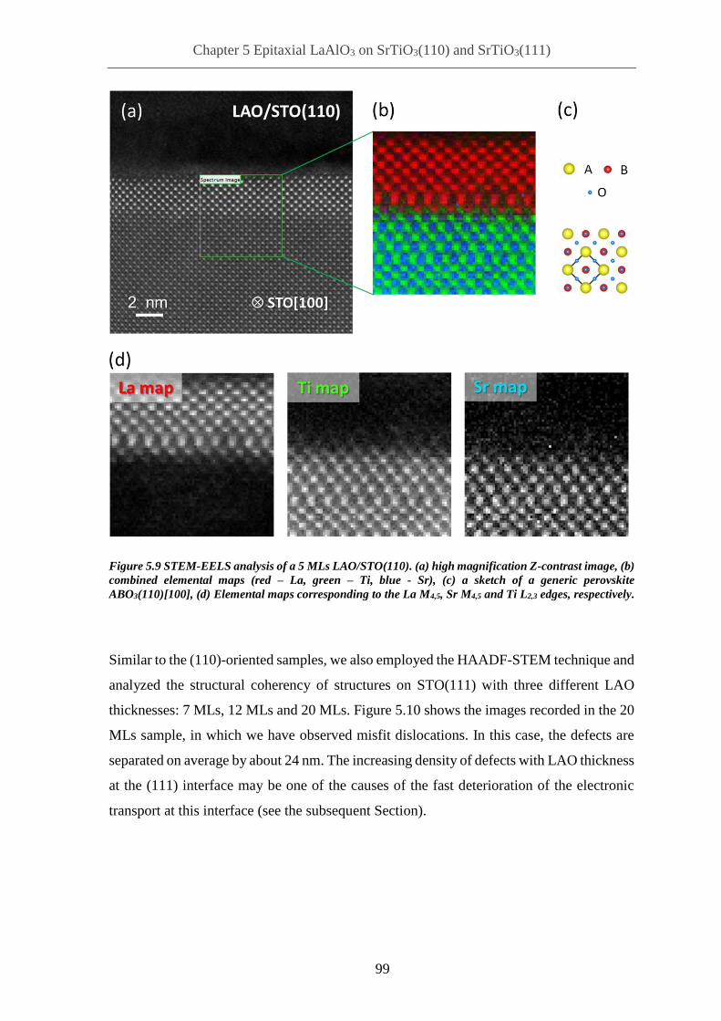
Chapter 5 Epitaxial LaAlO3 on SrTiO3(110) and SrTiO3(111)
99
Figure 5.9 STEM-EELS analysis of a 5 MLs LAO/STO(110). (a) high magnification Z-contrast image, (b)
combined elemental maps (red – La, green – Ti, blue - Sr), (c) a sketch of a generic perovskite
ABO3(110)[100], (d) Elemental maps corresponding to the La M4,5, Sr M4,5 and Ti L2,3 edges, respectively.
Similar to the (110)-oriented samples, we also employed the HAADF-STEM technique and
analyzed the structural coherency of structures on STO(111) with three different LAO
thicknesses: 7 MLs, 12 MLs and 20 MLs. Figure 5.10 shows the images recorded in the 20
MLs sample, in which we have observed misfit dislocations. In this case, the defects are
separated on average by about 24 nm. The increasing density of defects with LAO thickness
at the (111) interface may be one of the causes of the fast deterioration of the electronic
transport at this interface (see the subsequent Section).

Chapter 5 Epitaxial LaAlO3 on SrTiO3(110) and SrTiO3(111)
100
Figure 5.10 A high resolution HAADF-STEM image of 20 MLs LAO/STO(111) recorded along the [211]
zone axis with misfit dislocations marked in red (a), a inverse Fourier transformation of the same image
allowing fast localization of the defects (b), an image of one of the dislocations recorded at higher
magnification (c).
5.4. Electronic transport at the interfaces
The sample preparation and the measurement protocol to characterize the electric transport
of the LAO/STO interfaces are given in the Introduction. The resulting transport data
measured at room temperature of the LAO/STO grown on (110)- and (111)-oriented
substrates is shown in Figure 5.11. For the purpose of comparison, analogous set of data
for the conventional (001) interface has been taken from the literature [106,238] and added
to the figure. We can infer from the graphs that, regardless the substrate orientation, the
interfaces comprising thin enough layer of LAO are insulating or poorly conductive (> 10
MΩ). Above a certain critical thickness tc there is an onset of conductivity leading to similar
value of about 10-4 Ω-1 for all the interface orientations. The minimal critical thickness of
LAO depends on the substrate orientation: 7 MLs (~1.9 nm) for (110), nominally 8.6 MLs
(~1.9 nm) for (111) and 4 MLs (~1.5 nm) for the (001) samples, as previously reported in
the literature. As mentioned before, the (111)-oriented interfaces were grown always
together with the (110) ones, thus for the (111) orientation the growth nominally was not
stopped at full coverage of the last LAO monolayer. The thinner ~1.6 nm -nominally 7.3
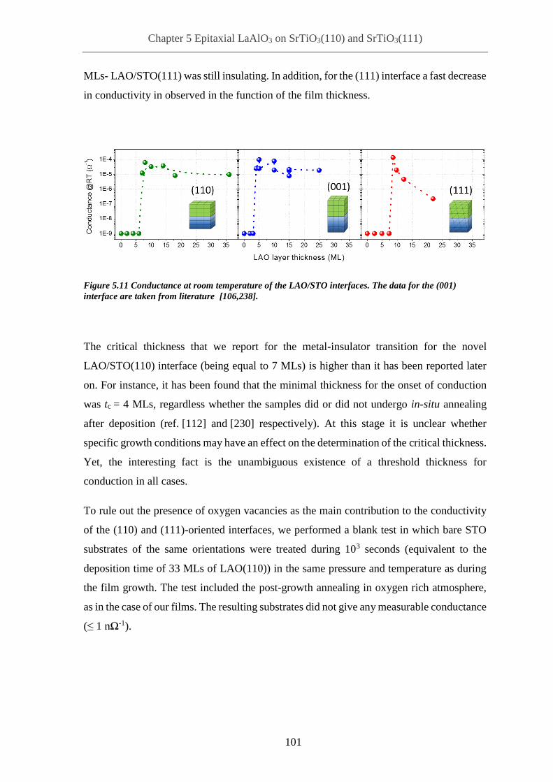
Chapter 5 Epitaxial LaAlO3 on SrTiO3(110) and SrTiO3(111)
101
MLs- LAO/STO(111) was still insulating. In addition, for the (111) interface a fast decrease
in conductivity in observed in the function of the film thickness.
Figure 5.11 Conductance at room temperature of the LAO/STO interfaces. The data for the (001)
interface are taken from literature [106,238].
The critical thickness that we report for the metal-insulator transition for the novel
LAO/STO(110) interface (being equal to 7 MLs) is higher than it has been reported later
on. For instance, it has been found that the minimal thickness for the onset of conduction
was tc = 4 MLs, regardless whether the samples did or did not undergo in-situ annealing
after deposition (ref. [112] and [230] respectively). At this stage it is unclear whether
specific growth conditions may have an effect on the determination of the critical thickness.
Yet, the interesting fact is the unambiguous existence of a threshold thickness for
conduction in all cases.
To rule out the presence of oxygen vacancies as the main contribution to the conductivity
of the (110) and (111)-oriented interfaces, we performed a blank test in which bare STO
substrates of the same orientations were treated during 103 seconds (equivalent to the
deposition time of 33 MLs of LAO(110)) in the same pressure and temperature as during
the film growth. The test included the post-growth annealing in oxygen rich atmosphere,
as in the case of our films. The resulting substrates did not give any measurable conductance
(≤ 1 nΩ-1).

Chapter 5 Epitaxial LaAlO3 on SrTiO3(110) and SrTiO3(111)
102
Figure 5.12 Sheet resistance of (left) LAO/STO(110) and (right) LAO/STO(111) interfaces.
The temperature-dependent resistivity for the samples above tc strongly depends on the film
orientation and thickness (Figure 5.12). For the (110) interfaces, the 8 MLs sample exhibit
a metallic behavior down to 5 K decreasing its sheet resistance from Rxx,RT ≈ 15 kΩ to Rxx,5K
≈ 0.16 kΩ. Above 10 MLs LAO thickness we can observe a progressive increase of
resistance with thickness and an upturn of resistivity at low temperatures. Above 18 MLs
electronic localization takes place at low temperatures. For instance the 36 MLs thick
sample changes its sheet resistance from Rxx,RT ≈ 1.1·105 kΩ at room temperature to Rxx,5K
≈ 4.6·106 kΩ at 5 K, thus a few orders of magnitude higher than in the case of the 8 MLs
sample. The degradation of transport properties with the LAO thickness has been also
observed for the conventional (001) LAO/STO interfaces – see e.g. ref. [238]. Concerning
the (111)-oriented interfaces, the thinnest conductive sample of (9 MLs) is metallic and
changes its sheet resistance from Rxx,RT ≈ 7.1 kΩ at room temperature to Rxx,5K ≈ 195 Ω at
5 K. Also in this case the transport characteristic of the sample changes rapidly with the
film thickness leading to poorly conductive interfaces above 10 MLs. It is evident that the
conductivity of the (111) interfaces deteriorate much faster compared to the (110)-oriented
counterparts, an observation that may be consistent with the emergence of misfit
dislocations, as observed from HAADF-STEM images (see Section 5.3. ).

Chapter 5 Epitaxial LaAlO3 on SrTiO3(110) and SrTiO3(111)
103
Figure 5.13 Sheet carrier density and mobility of the samples LAO/STO(110).
The evolution with temperature of the sheet carrier density and mobility for the (110)
interface (see Figure 5.13) brings more information about the transport properties at the
interface. At this point it is important to note, that the transverse resistance (Rxy) measured
in the Hall geometry for all the conductive samples was linear within the entire range of
applied magnetic field (±9 T) and temperature (5 K – 300 K), the sign of the slope of the
Rxy versus magnetic field indicating n-type conduction. For the considered series of
thickness, the sheet carrier density at 5 K ranges between nsheet,5k ≈ 1013 – 1014 cm-2, thus
similar to the values reported for conductive (001)-oriented interfaces. [82,100,234,238–
240] The slight increase of nsheet with temperature has also been reported for the classical
(001) interface. [238] The electron mobility at low temperatures exhibits larger variations
with the LAO thickness. For instance, 8 MLs yields at 5 K mobility of µ5k ≈ 680 cm2/Vs,
while for thicker 10 MLs µ5k ≈ 2500 cm2/Vs. Thicker layers results in lower electron
mobilities: µ5k ≈ 880 cm2/Vs for 14 MLs and µ5k ≈ 30 cm2/Vs for 18 MLs. This trend is
also known for the (001) interface, as indicated previously [238]. In overall, the measured
data results in a bell-shape curve of mobility vs. sheet carrier density, which is also
observed in the LAO/STO(001) interfaces [238] and doped STO [241].

Chapter 5 Epitaxial LaAlO3 on SrTiO3(110) and SrTiO3(111)
104
Figure 5.14 Resistance versus temperature of the samples with 10 MLs thick LAO deposited on an STO
substrate treated ex-situ (Samples A) or in-situ (Sample B).
We have also checked the influence of the substrate thermal treatment on the properties of
the 2DEG. For this purpose we have treated one STO(110) substrate in-situ in the PLD
chamber -prior the deposition- at 900 oC under 10-7 mbar of oxygen for 1 hour, followed
by cooling down to 550 oC and further annealing at this temperature and the base pressure
of 10-4 mbar for 1 hour. This procedure has been reported to yield a flat surface with the
morphology of steps and terraces. [226] The conditions of the subsequent deposition were
identical to the ones used by us for the standard substrates treated ex-situ in a dedicated
tubular furnace. The resulting LAO/STO samples display comparable resistance vs
temperature characteristics (Figure 5.14).
The STO(110) has in plane two orthogonal non-identical low index directions [001] and
[1-10] leading to the 2-fold symmetry. In the transport experiment described previously,
the current was applied along the [001] direction for this interface. However, in order to
examine any in-plane transport anisotropy we need to inject the current along two
orthogonal directions. For that purpose, we have deposited simultaneously two 9 MLs LAO
samples on two STO(110) substrates previously cut in a rectangular shape (2.5 x 5 mm2)
having the longer direction along [001] or [1-10]. Subsequently we wired the samples and
injected the current along the longer direction of the sample. As can be seen in the Figure
5.15, no obvious anisotropy could be observed. This observation is in agreement with
previous reports where no in-plane anisotropy was found for the samples deposited at the

Chapter 5 Epitaxial LaAlO3 on SrTiO3(110) and SrTiO3(111)
105
same oxygen pressure as the one used in this thesis. [230] Interestingly enough, the degree
of anisotropy in conductivity between the orthogonal [001] and [1-10] directions depends
not only on the deposition pressure, but also on the film thickness, making this effect visible
only for relatively thick LAO films. [242] This in turn brings the possibility of existence of
plastic relaxation above certain LAO thickness in the form of preferentially oriented
defects, not observed in our studies.
The findings reported here present many similarities between the most studied
LAO/STO(001) interface and the novel (110) and (111) interfaces reported here. This
includes the existence of the critical thickness for the metal-insulator transition and
comparable transport properties at different temperatures. At this point, one may speculate
whether there is a common origin for the 2DEGs emerging at these interfaces. Yet, our
present research does not allow giving a definitive answer to this question. Such enquiry is
especially relevant for the (110) interface, as in this case we don’t expect any polarity
discontinuity across the interface, at least not in the idealistic case. However, the real
picture may be more complex than that. For instance, the (110)-oriented surface of STO is
polar [243] and should by itself reconstruct to some extent prior to the deposition of the
LAO film. Yet, the details about this eventual ionic/electronic reconstruction are so far
unknown. This may leave open the option that the subsequent growth of a LAO overlayer
on top of a reconstructed STO (110) surface may give way to the existence of an interface
dipole triggered by the surface/interface reconstruction at the STO(110) surface, which
Figure 5.15 Temperature dependence of the sheet resistance of two samples with 9 MLs of LAO deposited
simultaneously. The current is injected along different direction for each sample.
10 10010
2
103
104
along:
[001]
[1-10]
She
et re
sis
tance (
)
Temperature (K)

Chapter 5 Epitaxial LaAlO3 on SrTiO3(110) and SrTiO3(111)
106
could influence the transport properties of the LAO/STO (110) interface. Of course, other
factors, also contemplated in the case of the (001) interface (ionic intermixing, vacancies),
may also play some sort of role. All in all, the physical mechanisms leading to the
emergence of a 2DEG at the (110) interface is an unresolved issue that would deserve an
intensive research activity in the future.
To summarize, our group has pioneered the investigation on the creation of 2DEGs at the
LAO/STO(110) and LAO/STO(111) interfaces, thus releasing the constraint of the
substrate orientation beyond the conventional and most studied (001) interface. The
creation of 2DEGs along interfaces other than (001) has given us the opportunity to probe
the effect of crystallographic orientation and the resulting electronic reconstructions on the
interface properties, which will be described briefly in the next sections. This, in turn, has
opened us the way toward a better understanding of the physics of these 2DEGs and its
interplay with the electronic orbital hierarchy, with implications in physical phenomena.
Indeed, a deep knowledge about all issues related to the electronic structure of LAO/STO
2DEGs is relevant for both fundamental and applied research. In this line, such a knowledge
should have an impact on the development of applications in electronics [138,244]. For
orientation other than (001), a better comprehension of the electronic structure is important
to understand transport anisotropy [245] or, in the case of (111) oriented interfaces, the
expectance of emergence of novel complex electronic phases [246]. Bearing this in mind,
we have undertaken the study of the electronic structure of the (110)-oriented interface.
The details of our research on the underlying electronic orbital reconstruction for this
interface are given briefly in the subsequent Section 5.5. On the other hand, the implications
of the orbital reconstruction on the 2D-character of superconductivity at the
LAO/STO(110) interface are discussed in Section 5.6.
5.5. Electron orbital reconstruction in LaAlO3/SrTiO3(110)
The previous Section showed many similarities in transport properties between LAO/STO
of the (001) and (110) orientation. Nevertheless, confining electrons along crystal planes
of different orbital symmetries should result, in principle, in distinct band reconstructions
with specific orbital hierarchies. This approach of tuning the orientation of quantum well

Chapter 5 Epitaxial LaAlO3 on SrTiO3(110) and SrTiO3(111)
107
structures is well known e.g. in the engineering of optoelectronic properties of III-V and II-
VI semiconductors. [247] An important question is whether the electronic structure of
2DEGs along the interfaces of LAO/STO (001) and (110) are really different. This is to
say, do they share a common orbital hierarchy or -on the contrary- a reconstruction of the
electronic band structure occurs when the orientation of the quantum well is changed.
In this Section we briefly present the highlights from our work exploring the connection
between orbitals’ symmetry and hierarchy. For this purpose, we used the room temperature
X-ray absorption spectroscopy (XAS) in total electron yield (TEY) mode. The data has
been collected at BOREAS beamline of the ALBA synchrotron radiation source 27. The
energy range was aimed at probing the Ti-L2,3 edges. In this case the L2 and L3 peaks in the
XAS spectra originate from the transitions between Ti-2p1/2 (L2) and Ti-2p3/2 (L3) core
levels to unoccupied Ti 3d states, respectively. As seen below, the fine structure of the L2,3
edges enabled us to investigate the t2g (dxz, dyx, dxy) and eg (dz2, dx2-y2) levels of the Ti.
Figure 5.16 Sketch of the interaction of linearly polarized light width d orbitals for normal (a, b) and
grazing (c, d) incidence of X-rays. The (001) interface is present in (a, c) and the (110) interface in (b, d).
The color shading listed in the box indicates the level of interaction.
27 https://www.cells.es/en/
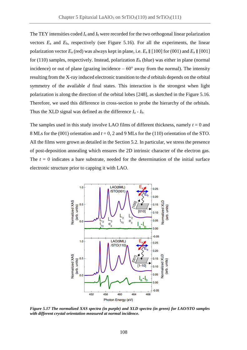
Chapter 5 Epitaxial LaAlO3 on SrTiO3(110) and SrTiO3(111)
108
The TEY intensities coded Ia and Ib were recorded for the two orthogonal linear polarization
vectors Ea and Eb, respectively (see Figure 5.16). For all the experiments, the linear
polarization vector Ea (red) was always kept in plane, i.e. Ea ∥ [100] for (001) and Ea ∥ [001]
for (110) samples, respectively. Instead, polarization Eb (blue) was either in plane (normal
incidence) or out of plane (grazing incidence – 60° away from the normal). The intensity
resulting from the X-ray induced electronic transition to the d orbitals depends on the orbital
symmetry of the available d final states. This interaction is the strongest when light
polarization is along the direction of the orbital lobes [248], as sketched in the Figure 5.16.
Therefore, we used this difference in cross-section to probe the hierarchy of the orbitals.
Thus the XLD signal was defined as the difference Ia - Ib.
The samples used in this study involve LAO films of different thickness, namely t = 0 and
8 MLs for the (001) orientation and t = 0, 2 and 9 MLs for the (110) orientation of the STO.
All the films were grown as detailed in the Section 5.2. In particular, we stress the presence
of post-deposition annealing which ensures the 2D intrinsic character of the electron gas.
The t = 0 indicates a bare substrate, needed for the determination of the initial surface
electronic structure prior to capping it with LAO.
Figure 5.17 The normalized XAS spectra (in purple) and XLD spectra (in green) for LAO/STO samples
with different crystal orientation measured at normal incidence.

Chapter 5 Epitaxial LaAlO3 on SrTiO3(110) and SrTiO3(111)
109
The XLD experiments done at normal incidence were performed to prove that the two
interfaces have different crystal orientations. The (001) samples have inherent fourfold in-
plane symmetry, thus light should be absorbed equally for both photon polarizations.
Indeed, the resulting XLD signal of the 8 MLs LAO/STO(001) sample is negligible (Figure
5.17 – top panel). In turn, in the case of the 9 MLs LAO/STO(110) sample the distinctive
nonzero XLD signal indicates the anisotropic character of this type of interface (bottom
panel).
On the other hand, the experiments at grazing incidence allow us to quantify the splitting
between the t2g and eg states and thus to define the orbital hierarchy. The numerical data
analysis was performed by dr. D. Pesquera 28 with the use of the CTM4XAS software [249].
The analyzed data are summarized in the Figure 5.18. The degeneracy of the t2g and eg
substates is already broken in the uncapped STO surfaces, which is caused by the symmetry
breaking at the interface. For instance, for the STO(110) surface, the dxy and dx2-y2 states
were found to be lower in energy compared to respectively the dxz/dyx and dz2 states, with
the level splitting of 20 meV and 10 meV for the eg and t2g states, respectively. Capping the
substrate with LAO results in the degeneracy breaking in the opposite direction. Here for
instance for the 9 MLs LAO/STO(110) the eg states are split by 50 meV and the t2g states
by 30 meV. In fact, such orbital hierarchy inversion with respect to bare surface is already
observed in 2 MLs LAO/STO(110), thus at the interface that do not exhibit any
macroscopic conductance. Similar finding has been reported for the (001) oriented
interface. [250] The somehow smaller splitting for the LAO/STO(001) interface obtained
28 Dr. David Pesquera is a former PhD student in our research group. http://departments.icmab.es/mulfox/
Figure 5.18 Sketched calculated energy splittings of d orbitals for (001)- and (110)-oriented samples.

Chapter 5 Epitaxial LaAlO3 on SrTiO3(110) and SrTiO3(111)
110
from our analysis compared to the one reported in ref. [250], may be a result of a different
sheet carrier density [251] reported in the two works.
The main result of our XLD study is the confirmation that the orbital electronic hierarchy
of the 2DEGs at the (110) interface is different than its counterpart at the (001) interface.
More precisely, we have observed that the order in which the electronic states appear as a
function of energy in the LAO/STO(110) interface is inverted with respect to the
LAO/STO(001) system. Thus, while dxy states are the lowest in energy for the (001)
oriented heterostructure, dxz/dyx states are instead at the bottom for the (110) interface.
Our results establish crystal symmetry as an extra degree of freedom to realize different
2DEG band reconstructions at this oxide interface. This in turn allows selective occupancy
of states of different symmetry and has implications on the 2D superconductivity at these
interfaces, as briefly discussed in the Section 5.6. The new way of engineering 2DEG paves
the way towards better understanding of the connection between orbital symmetry and
correlated states at the LaAlO3/SrTiO3 quantum well.
5.6. Electrostatic modulation of superconductivity in LaAlO3/SrTiO3(110)
It is well known that the 2DEGs at the LAO/STO(001) interface display superconductivity
at low temperatures (typically below about 300 mK). [100] The electrostatic tuning of the
carrier density in these samples has been shown to allow a diversity of complex phenomena,
including quantum phase transition from an insulating to a metallic state [106] or changes
of the critical temperature Tc for the onset of transition to a superconductive ground
state [104,252,253]. Electrostatic doping is a particularly interesting tool, as it permits
tuning the carrier density without the need of introducing additional structural defects like
e.g. oxygen vacancies.
Our discovery of 2DEGs at the (110) interface has opened a new perspective, as it allows
the study of the 2D superconductivity in a novel system that, as shown previously, displays
a different electron orbital hierarchy due to the different crystal symmetry. Additionally,

Chapter 5 Epitaxial LaAlO3 on SrTiO3(110) and SrTiO3(111)
111
electrostatic gating has allowed us the possibility of tuning the orbital occupation to
modulate the superconductive state.
As an illustrative example of how the different orbital hierarchy may affect a physical
property of the 2DEG, in the following we summarize concisely the outcome of low
temperature magnetotransport experiments done in collaboration with CNRS-ESPCI 29.
This study allowed the comparison of the superconductive properties of LAO/STO(001)
and (110) samples both grown in our laboratory.
For that purpose, a quantitative estimation of the superconductive layer thickness d was
done at the (110) interface using a Landau–Ginzburg formalism [123], as done with
previous reports on (001) [100,104,254]. The results of such analysis showed that the
superconductivity (110)-interface has a 2D character, confirming the bidimensional
character of the electronic system. Yet, beyond that, we also discovered that the anisotropy
of the 2D superconductive state is considerably larger for (001) than for (110), implying
that for the latter the superconductive thickness (d ≈ 24 – 30 nm) is larger than for the
former (d ≈ 10 nm), i.e., the spatial extension of the quantum well along (001) is smaller
than along (110) [123].
Intuitive reasoning based on fundamental quantum concepts gives a rationale for the
different spatial extent of the 2DEGs. More specifically, the rearrangement of orbital
symmetries observed for different crystal orientations change the carrier spatial
distributions of dxy, dxz and dyz states. Along (001) the first dxy sub-band is expected to be at
the bottom of the well, with little spatial spread; on the contrary, along (110) the dxy level
raises its energy above the dxz/dyz states, and its spatial extent is considerably larger (see
Figure 5.19). Therefore, the modulation of the orbital hierarchy provides a natural
explanation for the distinct anisotropy of the 2D superconductivity and spatial extension
for quantum wells oriented along (001) and (110) [123].
29 The collaboration was established with dr. N. Bergeal at the CNRS-ESPCI. https://www.espci.fr/en/

Chapter 5 Epitaxial LaAlO3 on SrTiO3(110) and SrTiO3(111)
112
Figure 5.19 Energy landscape of 2DEGs at (001) and (110) LAO/STO interfaces.
The different spatial extension of the 2DEGs at (001) and (110) interfaces was further
inferred by means of electrostatic gating experiments. For this purpose, a metallic back-
gate was made by depositing gold on the back side of the STO substrate. In the used
configuration, the polarity of the contacts is defined such that the “+” terminal is on the
back-gate electrode and the “-“ terminal is connected to the LAO/STO interface via
ultrasonic wire bonder with Al wires. Therefore, the positive/negative gate voltage Vg
corresponds, respectively, to accumulation/depletion of electrons at the interface. The
outcome of our low-temperature transport experiments is exemplified by the analysis of
two samples that were included in our study, namely a 14 MLs thick LAO/STO (110) and
a 10 MLs thick LAO/STO (001). In particular, the sheet resistance of these samples is
plotted as a function of temperature in the Figure 5.20 panels (a) and (b). An inspection of
these figures clearly reveals that the superconductive state can be suppressed in the
LAO/STO(001) interface for both large enough negative or positive applied gate voltages.
In contrast, for the (110) interface, the superconductivity cannot be suppressed for any
value of the gate voltage range used in this study (Vg = ± 400 V). The panel (c) of Figure
5.20 features the summary of these electrostatic gating experiments. Here, again, we can
see that the superconductivity in the (001) interface can be suppressed by applied voltage
(with agreement to the previous reports, e.g. [104,252]), while the Tc of the (110) interface
changes within the used Vg range of at most only ≈ 50 %.
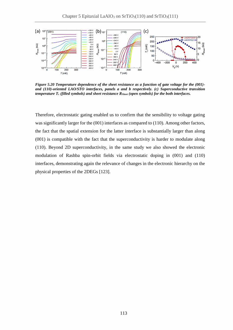
Chapter 5 Epitaxial LaAlO3 on SrTiO3(110) and SrTiO3(111)
113
Figure 5.20 Temperature dependence of the sheet resistance as a function of gate voltage for the (001)-
and (110)-oriented LAO/STO interfaces, panels a and b respectively. (c) Superconductive transition
temperature Tc (filled symbols) and sheet resistance RSheet (open symbols) for the both interfaces.
Therefore, electrostatic gating enabled us to confirm that the sensibility to voltage gating
was significantly larger for the (001) interfaces as compared to (110). Among other factors,
the fact that the spatial extension for the latter interface is substantially larger than along
(001) is compatible with the fact that the superconductivity is harder to modulate along
(110). Beyond 2D superconductivity, in the same study we also showed the electronic
modulation of Rashba spin-orbit fields via electrostatic doping in (001) and (110)
interfaces, demonstrating again the relevance of changes in the electronic hierarchy on the
physical properties of the 2DEGs [123].


115
Chapter 6 The interface between amorphous oxides and SrTiO3(110) and (111)
Part of the work discussed in this chapter was later published in:
M. Scigaj, J. Gázquez, M. Varela, J. Fontcuberta, G. Herranz, and F. Sánchez, “Conducting
interfaces between amorphous oxide layers and SrTiO3(110) and SrTiO3(111)” Solid State
Ionics 281, 68 (2015).

Chapter 6 The interface between amorphous oxides and SrTiO3(110) and (111)
116
Abstract
The deposition of amorphous oxides of LaAlO3 (a-LAO), Y:ZrO2
(a-YSZ) and SrTiO3 (a-STO) on (110) and (111) STO single
crystals yields conductive interfaces. The relative importance of the
(I) oxygen affinity of the deposited metals versus (II) the
orientation-dependent energy of vacancy formation and diffusion
on the creation of oxygen vacancies is judged. Our study reveals
that the oxygen affinity of the deposited atomic species, rather than
the difference in the energy of oxygen vacancy formation, is the
main factor governing the creation of oxygen vacancies and
consequently the appearance of interface conductivity.

Chapter 6 The interface between amorphous oxides and SrTiO3(110) and (111)
117
In the previous Chapter we have shown how choosing a particular orientation of the
substrate can be used to modulate properties of the 2DEG at the interface between epitaxial
LAO on STO. It is also known that growing certain amorphous oxides on the STO(001)
may also result in a conductive interface (e.g. [118,130–135]), where the film critical
thickness for the onset of conductivity tc is a function of the deposition pressure [118,131].
In this case it is widely accepted that oxygen vacancies at the interface give the origin to
the charge carriers. The strong influence of the nominal chemical composition of the
amorphous overlayer on the tc is usually explained by different affinity of the constituting
metallic elements to oxygen. Herein an interesting question arises concerning the potential
influence of the substrate crystal orientation on the process of oxygen vacancy formation
and therefore the electronic properties at the interface. In this Chapter we take a closer look
at this concept by analyzing the transport properties of conductive interfaces generated by
depositing amorphous oxides on top of (110) and (111) oriented STO crystals.
6.1. Growth of the amorphous layers
A series of amorphous films of LaAlO3 (a-LAO), Y:ZrO2 (a-YSZ, with ~7 % molar of
Y2O3) and STO (a-STO) has been deposited within the thickness range of 1-8 nm. All the
layers were grown on the STO (110) substrate. In particular, the a-LAO films were grown
simultaneously on both (110)- and (111)-oriented STO substrates. All the single crystals
were thermally treated as explained in the Section 5.1. in order to obtain a morphology of
steps and flat terraces. [121] In addition to this, prior to the deposition, each substrate was
heated in-situ in the PLD chamber up to 500 oC at PO2 = 0.5 mbar oxygen pressure to
eliminate the adsorbates. Subsequently the substrate was cooled overnight to room
temperature at PO2 = 200 mbar to eliminate the presence of oxygen vacancies. All the
amorphous films were deposited at room temperature. Apart from this, other growth
conditions were identical to these used for the epitaxial LAO, as stated in the Section 5.2. ,
namely: PO2 = 10-4 mbar, 1 Hz laser repetition rate, substrate-target distance of 60 mm and
the laser pulse energy and fluence of about 26 mJ and 1.5 J/cm2, respectively.

Chapter 6 The interface between amorphous oxides and SrTiO3(110) and (111)
118
Figure 6.1 RHEED patterns acquired at room temperature at the incident angle of about 0.9o taken along
[001] with respect to STO(110) at the end of the growth. The very last graph presents the direct electron
beam without any sample mounted.
The growth of all the amorphous layers was monitored by RHEED. All resulting images
(see examples in Figure 6.1) indicate a diffused-like halo without any Bragg reflections, in
perfect agreement with the amorphous nature of the deposited films. The apparent arc is a
sample-independent artifact visible at high electron beam intensities (see the last panel on
the right in Figure 6.1).
6.2. Electronic transport properties
In order to measure transport properties, all the conductive interfaces were contacted via
ultrasonic wire bonding with aluminum wires. The resistance was measured by injecting
current along the in-plane STO [110] direction in the (110)-interfaces, and along STO [11-
2] in the (111)-interfaces.
For each of the a-LAO, a-YSZ and a-STO series a critical thickness tc has been observed
above which a metallic conduction can be measured. Selected examples of the sheet
resistance Rs versus temperature curves for each series are depicted in Figure 6.3. Here can
be seen that each interface features metallic-like behavior upon cooling down to about 10
K, were slight upturn may appear (in panels (b) and (c)). As discussed in the previous
Chapter, similar resistivity upturns have been also reported in crystalline interfaces. [255]
The overall resistance-temperature characteristic, as well as the room temperature values,
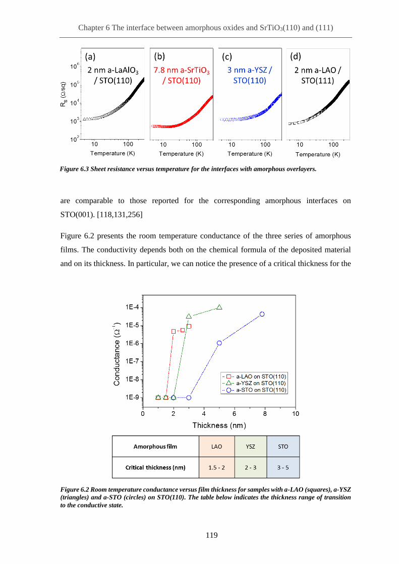
Chapter 6 The interface between amorphous oxides and SrTiO3(110) and (111)
119
are comparable to those reported for the corresponding amorphous interfaces on
STO(001). [118,131,256]
Figure 6.2 presents the room temperature conductance of the three series of amorphous
films. The conductivity depends both on the chemical formula of the deposited material
and on its thickness. In particular, we can notice the presence of a critical thickness for the
Figure 6.2 Room temperature conductance versus film thickness for samples with a-LAO (squares), a-YSZ
(triangles) and a-STO (circles) on STO(110). The table below indicates the thickness range of transition
to the conductive state.
Figure 6.3 Sheet resistance versus temperature for the interfaces with amorphous overlayers.

Chapter 6 The interface between amorphous oxides and SrTiO3(110) and (111)
120
onset of conductivity tc (see the table). For instance, growing 1.5 nm thick a-LAO on
STO(110) results in an insulating interface, whereas a sample with 2.0 nm thick a-LAO is
conductive. Interestingly enough, we observe that the critical thickness tc of the amorphous
a-LAO and the epitaxial c-LAO (7 MLs, thus ~1.9 nm) on STO(110) is practically identical.
Yet, this coincidence may be purely accidental, as it is known that the tc of different
amorphous overlayers grown on STO(001) depend on the growth conditions, especially
oxygen pressure [131]. However, since all the samples analyzed in this study were grown
using the same parameters of temperature and oxygen partial pressure and the transport
characterization was carried out in the same conditions, we can identify a robust trend
regarding the value of the critical thickness in relation to the material used as amorphous
oxide. In particular, we observe that for amorphous layers on STO(110) the following
relationship holds: tc(a-LAO) < tc(a-YSZ) < tc(a-STO). It is important to note that the same
trend has been observed for amorphous films deposited by PLD on the
STO(001). [131,256]
In the literature of the topic there is a general consensus that the conduction at the interfaces
between amorphous films and STO substrates has its origin in oxygen vacancies in STO
created upon deposition of the amorphous film. In this regard, several mechanisms resulting
in the creation of the conductive interface have been proposed. In particular, metal species
(e.g. arriving on the surface with a PLD plasma plum) may get oxidized by extracting an
oxygen from the substrate. [131,256] A general thermodynamic condition for the
occurrence of this red-ox process at the surface of STO is that the heat of formation of the
resulting oxide per mole of oxygen should be lower than -250 kJ/(mol O). [257] Other
condition results from the consideration of the space charge created at the interface between
the just deposited metal and substrate (semiconductor); this in turn is determined by the
interface electronic configuration, i.e. the relative energy of the Fermi levels of the metal
and the oxide before the contact. Thus the most favorable condition of the red-ox reaction
is when the work function of the metal is in the range 3.75 eV < φ < 5.0 eV. [131,257]
Other necessary considerations involve the exact composition of the plume which reached
the STO surface as well as the kinetic energy of the constituting entities. This energy
modulates the kinetics of the red-ox reaction by means of the energetic impact of the fast
oxygen deficient species (≥ 1 eV). [133] The plume composition and energy is governed
by the laser fluence and wavelength, the optical properties of the deposited material, the
pressure and composition of the gas during the deposition and the target-substrate distance.

Chapter 6 The interface between amorphous oxides and SrTiO3(110) and (111)
121
In turn, the onset of conductivity has been described in terms of the percolation of the
electrons associated with the oxygen vacancies, that increase in number upon the
amorphous film growth. [118]
Figure 6.4 Room temperature conductance versus thickness of a-LAO films on STO(110) (open rhombi)
and STO(111) (solid rhombi).
In principle, the oxygen vacancy creation via chemical reaction at the interface should
depend on two factors: (1) the oxygen affinity of the PLD plasma species upon arrival at
the substrate surface and (2) the energy of vacancy creation and diffusion being dependent
on the crystallographic orientation of the substrate’s surface. Our experiments revealed the
same critical thickness of tc = 2 nm for a-LAO on the both (110) and (111) STO orientations
(see Figure 6.4). Knowing this and the previously indicated relation between tc and the
films chemistry, we can conclude that in fact the ability to create oxygen vacancies is
dictated by the type of the deposited material. In other words, the inherent properties of the
growing film dominate and overrule the distinct energies of oxygen vacancy formation and
diffusion in each surface, therefore controlling the basic transport properties at the
interface.
0 2 4 6 8 10
10-9
10-8
10-7
10-6
10-5
10-4
a-LAO/STO(111)
a-LAO/STO(110)
Co
ndu
cta
nce
(
)
Thickness (nm)

Chapter 6 The interface between amorphous oxides and SrTiO3(110) and (111)
122
6.3. Thermodynamic considerations
The experimental findings described in the previous Section stress the importance of the
chemical red-ox reactions on the formation of the conductive interface between amorphous
films and an STO substrate. In order to better understand the relation between the critical
thickness and the film chemistry, we will consider the change of the Gibbs energy for the
oxidation reaction of each of the constituting cations. The free energy of formation of
La2O3, Al2O3, ZrO2, Y2O3, SrO and TiO2 are accordingly: −1795.4 kJ/mol, −1581.7 kJ/mol,
−1039.4 kJ/mol, −1816.1 kJ/mol, −561.2 kJ/mol and −889.1 kJ/mol, at 300 K. [258] Here
the key phenomena is the formation of the oxygen vacancy, thus we have to normalize
these values to one mole of oxygen. [32] Finally, we have to consider the molar
concentration of each oxide in the binary composition of the film. This leads to the weighted
Gibbs energies of La2O3-Al2O3, (ZrO2)0.93-(Y2O3)0.07 and SrO-TiO2 as −1125.7 kJ/mol O2,
−1051.4 kJ/mol O2 and −1005.7 kJ/mol O2, respectively. An example of these simple
calculations is given below.
Figure 6.5 The calculation of weighted Gibbs energy ∆G of YSZ.
Of course, this is a very simple analysis and does not take into account the different
consumption of cations upon the substrate reduction.
Using the above-mentioned model, we can plot in Figure 6.6 the critical thickness for each
material series versus the corresponding weighted Gibbs energy. The vertical error bars
correspond to the range of thickness of each amorphous layer: the highest among insulating
interfaces and the lowest among conductive interfaces. We can see that the critical thickness
increases as the energy of oxide formation decreases in magnitude. This relation strongly
supports the correlation between the presence of oxygen vacancies in the STO substrate

Chapter 6 The interface between amorphous oxides and SrTiO3(110) and (111)
123
and the metal-insulator transition. The simple model proposed here based on
thermodynamic considerations could alone explain the experimentally observed relation
tc(a-LAO) < tc(a-YSZ) < tc(a-STO) without invoking the substrate crystallographic
orientation.
6.4. Electron microscopy studies of the interface
In order to gain a better understanding of the structure and chemical composition at the
conductive interface featuring an amorphous film, we conducted STEM-EELS studies30 on
a sample a-LAO/STO(110) comprising nominally 4.8 nm think amorphous overlayer. The
low magnification image in Figure 6.7 (a) shows a coherent interface with the film of
uniform thickness. The high magnification Z-contrast image in panel (b) indicates bright
atomic columns of the STO substrate along the [100] zone axis, as illustratively sketched
in the panel (g). On the other hand, no long atomic order can be seen in the a-LAO layer,
indicating its amorphous character. Just at the interface we spot an interfacial layer -being
30 The images were recorded by dr. Jaume Gázquez, a scientist working at ICMAB-CSIC, in collaboration
with the STEM Group of the Oak Ridge National Laboratory (http://stem.ornl.gov/).
Figure 6.6 Critical thickness of a-LAO, a-YSZ and a-STO films on STO(110) plotted against the Gibbs
energy estimated from binary oxides of the cations present in each layer.

Chapter 6 The interface between amorphous oxides and SrTiO3(110) and (111)
124
up to 0.5 nm in thickness- with ordered atomic columns of high intensity. This indicates a
presence of certain crystalline phase rich in heavy La atoms. A similar observation was
made for the a-LAO/STO(001) interface, however without any further analysis. [118]
Figure 6.7 STEM cross section view of a nominally 4.8 nm thick a-LAO/STO(110) along the STO[001]
zone axis: (a) low and (b) high magnification Z-contrast image of the interface. The square marks the area
where the spectrum image was acquired. (c–e) Elemental maps corresponding to the La M4,5, Sr M4,5 and
Ti L2,3 edges, respectively. (f) RGB map produced by overlaying the Sr (in red), La (green) and Ti (blue).
(g) A scheme showing defects-free STO perovskite structure along the [001] direction. (h) and (i) show a
set of Ti L edge spectra from STO seven unit cells away from the interface (in black), two unit cells from
the interface (blue) and the at the interface (red) of epitaxial and amorphous grown LAO/STO(110)
samples, respectively.
To get a better insight into the nature of the observed atomically thin crystalline interfacial
layer we recorded atomic resolution maps of the La M4.5, Sr M4.5 and Ti L2.3 edges, see
Figure 6.7 (c-e). The combined image in the panel (f) indicates that the bright phase
contains La, Ti and Sr. Taking into account that: (I) a typical loss of kinetic energy of
ablated species penetrating matter is in the order of 100 eV/nm [259] and that (II) the
maximum kinetic energy of La species in the PLD plume at the used by us PO2 was reported

Chapter 6 The interface between amorphous oxides and SrTiO3(110) and (111)
125
to be about 58 eV [260], we can speculate that the La-rich interfacial layer might be the
result of the impinging species on the STO substrate. We stress that the crystalline La-rich
layer is not thicker than 0.5 nm, thus much below the tc reported for crystalline
LAO/STO(110) stacking (tc = 7 MLs, thus ~1.9 nm). Therefore, the metallic behavior
observed in the amorphous/SrTiO3 interfaces cannot be originated by this crystalline layer.
On the other hand, it is known that while unstrained stoichiometric LaTiO3 is a Mott
insulator [120], the La1−xSrxTiO3 solid solution is metallic for the wide doping range of
0.05 < x < 0.95 [116,117]. Nevertheless, the clear lack of coherence in this layer strongly
suggests that its direct contribution into conductivity is negligible. Other important
experimental findings proving this hypothesis and instead pointing out to the presence of
oxygen vacancies as the origin of the metallic behavior are given in the Section 6.5.
Indeed, the concentration of oxygen vacancies at the interface is of key importance for the
creation of conducting interfaces with amorphous overlayers. EEL spectroscopy allows us
to get a better idea about the presence of this kind of defects, by analyzing the shape of the
Ti L edge. This is possible as oxygen vacancies transfer electrons to Ti d bands, while the
fine structure of the Ti L edge changes as the oxidation state of Ti shifts from 4+ to lower
values. [261,262] Figure 6.7 (h) and (i) depicts the fine structure of the Ti L edge for
epitaxial and amorphous LAO-based samples. Colors indicate the distance from the
interface: seven unit cells (in black), two unit cells (blue) and at the interface (red). The
change of the relative intensity of the peaks as a function of the distance from the interface
is much more pronounced for the sample featuring amorphous LAO. This is an indication
of the higher presence of Ti3+ at this interface, which is in full agreement with higher
concentration of oxygen vacancies at the amorphous layer interface compared to the
epitaxial layer interface.
6.5. The role of oxygen vacancies
The presence of oxygen vacancies can be indirectly inferred by analyzing a change in the
interface conductivity upon heating the sample in an oxygen-rich atmosphere. Needless to
say, re-oxygenation induces the filling of vacancy defects, so that mobile carriers are
removed leading to an increase in resistance. To compare the effect of oxygen-rich

Chapter 6 The interface between amorphous oxides and SrTiO3(110) and (111)
126
annealing in the transport properties of amorphous and epitaxial LAO films, we measured
two samples grown on STO(110) with the very similar thickness of nominally 2.6 nm and
9 MLs (~2.4 nm), respectively. The sheet resistance of both the crystalline and amorphous
samples was measured in-situ during annealing in ambient in the 4-probe configuration.
The heating and cooling rate was set to 5.2 °C/min. The results are presented in Figure 6.8
left panel. For the interface featuring amorphous LAO (open circles) we can appreciate a
rapid increase of resistivity starting from above ~100 °C. The overall shape of this trend
resembles a percolation mechanism, where -in this case- conducting areas at the interface
emerge, enlarge and subsequently start overlapping leading to a gradual decrease in
resistivity. [118] Similar behavior has been reported for analogous interfaces on
STO(001). [118,131,263] In contrast, the change of resistance of the crystalline LAO with
the annealing is much smaller. The relatively small variation in resistance in the epitaxial
film might be attributed to filling of residual oxygen vacancies that could remain from the
first annealing done in-situ after the PLD deposition. Therefore, this simple experiment
hints at the different origin of the 2DEG for the amorphous and crystalline types of
interfaces, and underpins the central role of oxygen vacancies as generators of mobile
carriers in the amorphous samples.
Figure 6.8 On the left, a resistance measured in a 4-probe configuration in air versus the temperature. On
the right., a resistance of a 5 nm a-STO/STO(110) sample measured in a 2-probe configuration in air
versus the amount of days past after the sample deposition.
In fact, it turns out that the conductivity of the samples featuring amorphous films is not
stable over time if the samples are stored in ambient conditions. An illustrative example is

Chapter 6 The interface between amorphous oxides and SrTiO3(110) and (111)
127
given in Figure 6.8 (right panel) for a sample with 5 nm thick a-STO film. We can
appreciate a clear exponential increase of resistance till the measurement limit. The decay
time depends on the sample thickness (as also reported for a-LAO/STO(001) [264]) and on
the type of the deposited material. This indicates that the presence of oxygen vacancies in
STO -at densities enabling formation of conductive interface- is thermodynamically
unfavorable and the resulting increase of resistivity is in this case kinetically limited by the
distinct oxygen permeability of the deposited overlayers.
6.6. Conclusions
In this Chapter we analyzed the conductive interfaces between amorphous oxides and
STO(110) and STO(111) surfaces. It turns out that the critical thickness for the onset of
conduction tc does not depend on the substrate orientation. On the other hand, a strong
influence of the deposited film chemistry on the tc has been found, where tc decreases with
the magnitude of change of the Gibbs energy of oxide formation. Thus, the oxygen affinity
of the deposited atomic species, rather than the difference in the energy of oxygen vacancy
formation in diffusion in different crystallographic planes, is the main factor governing the
creation of these defects and consequently the appearance of 2DEG above tc. Moreover,
the presence of oxygen vacancies at the interface in a-LAO/STO(110) has been confirmed
directly by STEM-EELS and indirectly by the temperature and time resistance tests.


129
Chapter 7 YSZ(001)/SrTiO3(110): symmetry discontinuity study
Part of the work discussed in this chapter was later published in:
M. Scigaj, N. Dix, M. Cabero, A. Rivera-Calzada, J. Santamaria, J. Fontcuberta, G.
Herranz, and F. Sánchez, “Yttria-stabilized zirconia/SrTiO3 oxide heteroepitaxial interface
with symmetry discontinuity” Applied Physics Letters 104, 251602 (2014).

Chapter 7 YSZ(001)/SrTiO3(110): symmetry discontinuity study
130
Abstract
Herein we demonstrate a layer-by-layer growth of YSZ(001) on
STO(110), establishing a single domain interface between these
two dissimilar materials. The epitaxial relationship can be
expressed as [110]YSZ(001)//[001]SrTiO3(110). Therefore, this
interface features a symmetry discontinuity in the interface plane
and a discontinuity of atomic planes stacking across it. We stress
that our growth strategy, based on the use of substrates with lower
crystal symmetry, paves the way towards the development of other
innovative oxide interfaces.

Chapter 7 YSZ(001)/SrTiO3(110): symmetry discontinuity study
131
7.1. Growth conditions
Prior to film deposition, the STO(110) substrates were treated in a dedicated furnace at
1100ºC for 2 h in air in order to obtain the morphology of terraces and steps [121,225]. The
YSZ films were grown by pulsed laser deposition (KrF excimer laser, λ = 248 nm) assisted
with high pressure RHEED setup (30 kV). The heating up of the substrates to the deposition
temperature (850ºC) was done at oxygen partial pressure PO2 = 0.1 mbar. The YSZ
deposition conditions were: PO2 = 10-4 mbar, 1 Hz repetition rate, the substrate-target
distance of 60 mm and the laser pulse energy of about 26 mJ. The RHEED in-situ analysis
was done with the electron beam incidence angle of around 0.9º along the STO[001]
direction. The prepared films are of thickness of 16, 32 and 64 monolayers (MLs), which
corresponds accordingly to 8, 16 and 32 unit cells of the fluorite YSZ structure. The cooling
procedure involved PO2 = 0.3 mbar from 850ºC to 750ºC and PO2 = 200 mbar from 750ºC
to room temperature with a dwell time of 1 hour at 600ºC.
7.2. In-situ epitaxy studies using RHEED
The RHEED pattern of the STO(110) substrate prior the deposition exhibits a high intensity
specular spot, Bragg spots on the 0th Laue circle and Kikuchi lines (Figure 7.1 (a))
indicating a high quality surface. Here we also can note the presence of additional Bragg
spots originating from the x2 type reconstruction along the [1-10] direction. This is not
surprising as it has been calculated that the (1x2)(110) surface reconstruction for SrTiO3
has the lowest energy, comparable to its (001) surface energy. [265] The RHEED
oscillations of the specular spot intensity were observed since the very beginning of each
deposition (Figure 7.1 (e)). This observation indicates the layer-by-layer growth mode of
the YSZ film. The low intensity of the first few oscillations is a common feature in the
heteroepitaxial growth [255,266,267] and is likely caused by the interference of the
electron beams reflected from the film surface and from the substrate buried in the interface.
In case of the 64 MLs-thick sample, the overall intensity is relatively lower, most probably
due to slightly different acquisition conditions (horizontal arrows indicate the increase of
the electron beam current from the RHEED gun). This in turn results in very weak

Chapter 7 YSZ(001)/SrTiO3(110): symmetry discontinuity study
132
amplitude of oscillations at the end of the growth (not shown here). In this case the growth
was stopped after the nominal amount of pulses deduced from the growth rate.
Nevertheless, the RHEED pattern at the end of the deposition (64 MLs) was streaky
signalizing epitaxial growth and surface flatness (Figure 7.1 b).
Figure 7.1 (a) RHEED pattern of an STO(110) substrate, taken along STO[001] at room temperature and
base pressure. (b) RHEED pattern at the end of the growth of the 64 MLs-thick YSZ film, taken along
YSZ[110] at 850 OC under PO2 of 10-4 mbar. (c) and (d) were taken along YSZ[-110] and [010], respectively,
at room temperature and base pressure, after air exposure of the sample. In the panels (c) and (d) attached
is the simulation of the first order streaks of YSZ(001)[-110] and YSZ(001)[010], accordingly. (e) Intensity
of the RHEED specular spot during deposition of YSZ films: 16 ML, 32 ML, and 64 ML; in the last case
only data corresponding to the beginning of the growth is shown, with the horizontal black arrows

Chapter 7 YSZ(001)/SrTiO3(110): symmetry discontinuity study
133
indicating where the intensity of the primary electron beam was increased manually. Vertical arrows
indicate the end of the deposition of the 16 and 32 ML films.
Figure 7.1 presents RHEED patterns of YSZ recorded after growth along different
crystallographic directions. The great similarity between the patterns recorded along the
[110] and [-110] orthogonal directions (panels (b) and (c), respectively), together with the
presence of a substantially different pattern recorded along the bisecting angle ([010], panel
(d)) indicates the presence of the four-fold symmetry in the surface plane of the YSZ film,
thus higher than the two-fold symmetry of the (110)-oriented STO substrate. Moreover, our
experimental data are in perfect agreement with the simulated31 patterns for the YSZ cell
oriented as [110]YSZ(001)||[001]SrTiO3(110), shown in Figure 7.1 (c) and (d). In the next
subsection more details will be given on the epitaxial relationship between the film and the
substrate based on the XRD data recorded ex-situ.
Figure 7.2 The evolution of spacing between Bragg streaks on RHEED pattern (recalculated to real space)
of a 16.5 nm YSZ film along the deposition.
An evolution of the RHEED pattern upon film growth can be recorded and the spacing
between the Bragg’s streaks k as a function of the film thickness can be extracted. This
reciprocal space value carries the information about the in-plane cell dimension in real
31 The simulation was made using the RHEEDsim [268] code. The program calculates the position and
intensity modulation of first order RHEED streaks using a simplified kinematic approach.
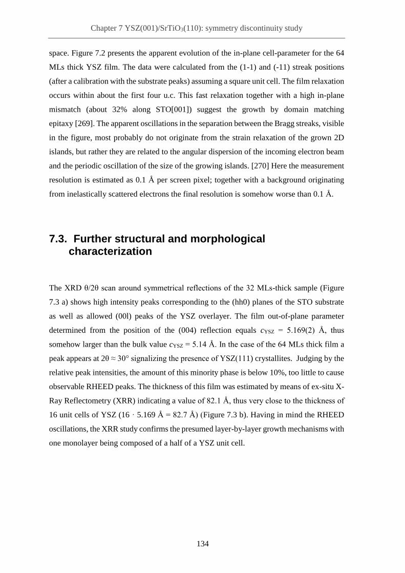
Chapter 7 YSZ(001)/SrTiO3(110): symmetry discontinuity study
134
space. Figure 7.2 presents the apparent evolution of the in-plane cell-parameter for the 64
MLs thick YSZ film. The data were calculated from the (1-1) and (-11) streak positions
(after a calibration with the substrate peaks) assuming a square unit cell. The film relaxation
occurs within about the first four u.c. This fast relaxation together with a high in-plane
mismatch (about 32% along STO[001]) suggest the growth by domain matching
epitaxy [269]. The apparent oscillations in the separation between the Bragg streaks, visible
in the figure, most probably do not originate from the strain relaxation of the grown 2D
islands, but rather they are related to the angular dispersion of the incoming electron beam
and the periodic oscillation of the size of the growing islands. [270] Here the measurement
resolution is estimated as 0.1 Å per screen pixel; together with a background originating
from inelastically scattered electrons the final resolution is somehow worse than 0.1 Å.
7.3. Further structural and morphological characterization
The XRD θ/2θ scan around symmetrical reflections of the 32 MLs-thick sample (Figure
7.3 a) shows high intensity peaks corresponding to the (hh0) planes of the STO substrate
as well as allowed (00l) peaks of the YSZ overlayer. The film out-of-plane parameter
determined from the position of the (004) reflection equals cYSZ = 5.169(2) Å, thus
somehow larger than the bulk value cYSZ = 5.14 Å. In the case of the 64 MLs thick film a
peak appears at 2θ ≈ 30° signalizing the presence of YSZ(111) crystallites. Judging by the
relative peak intensities, the amount of this minority phase is below 10%, too little to cause
observable RHEED peaks. The thickness of this film was estimated by means of ex-situ X-
Ray Reflectometry (XRR) indicating a value of 82.1 Å, thus very close to the thickness of
16 unit cells of YSZ (16 · 5.169 Å = 82.7 Å) (Figure 7.3 b). Having in mind the RHEED
oscillations, the XRR study confirms the presumed layer-by-layer growth mechanisms with
one monolayer being composed of a half of a YSZ unit cell.
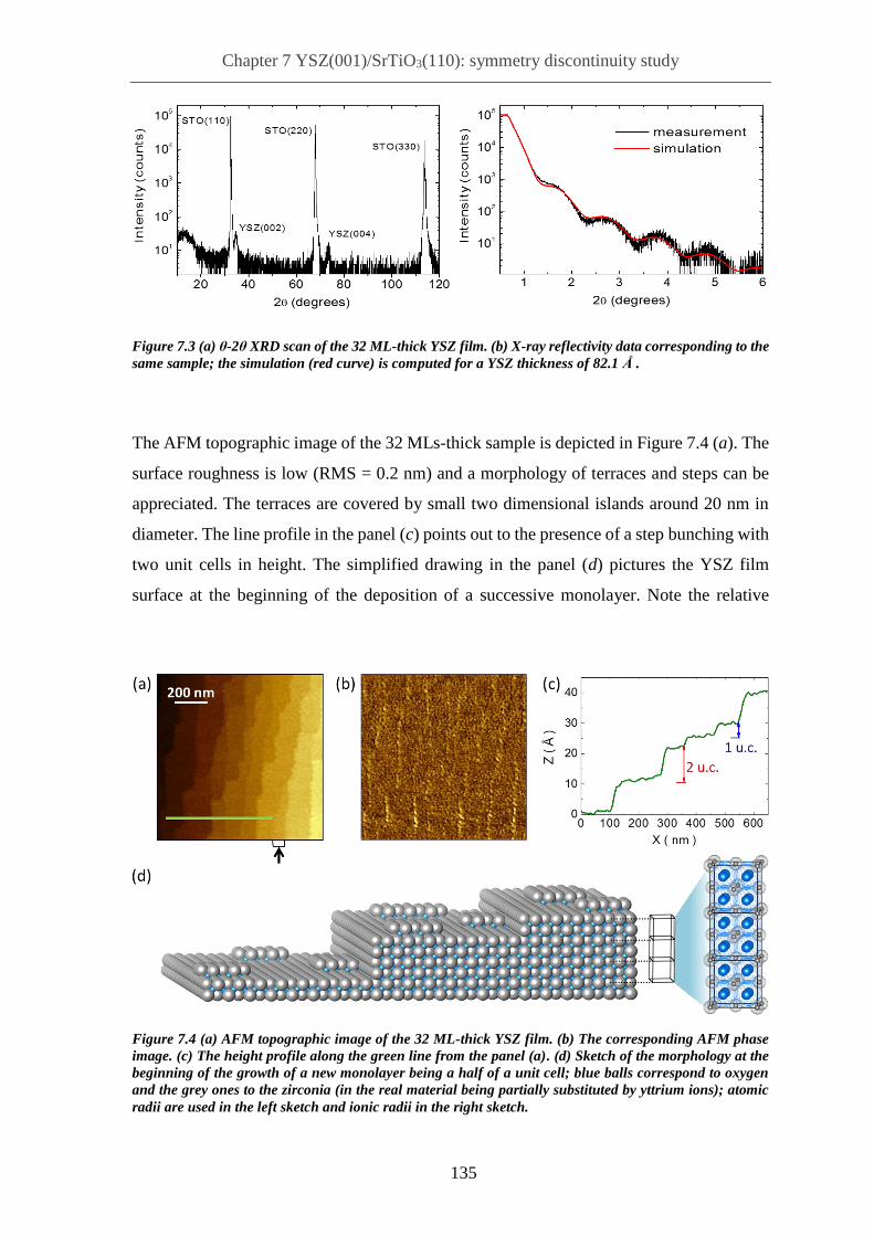
Chapter 7 YSZ(001)/SrTiO3(110): symmetry discontinuity study
135
Figure 7.3 (a) θ-2θ XRD scan of the 32 ML-thick YSZ film. (b) X-ray reflectivity data corresponding to the
same sample; the simulation (red curve) is computed for a YSZ thickness of 82.1 Å .
The AFM topographic image of the 32 MLs-thick sample is depicted in Figure 7.4 (a). The
surface roughness is low (RMS = 0.2 nm) and a morphology of terraces and steps can be
appreciated. The terraces are covered by small two dimensional islands around 20 nm in
diameter. The line profile in the panel (c) points out to the presence of a step bunching with
two unit cells in height. The simplified drawing in the panel (d) pictures the YSZ film
surface at the beginning of the deposition of a successive monolayer. Note the relative
Figure 7.4 (a) AFM topographic image of the 32 ML-thick YSZ film. (b) The corresponding AFM phase
image. (c) The height profile along the green line from the panel (a). (d) Sketch of the morphology at the
beginning of the growth of a new monolayer being a half of a unit cell; blue balls correspond to oxygen
and the grey ones to the zirconia (in the real material being partially substituted by yttrium ions); atomic
radii are used in the left sketch and ionic radii in the right sketch.

Chapter 7 YSZ(001)/SrTiO3(110): symmetry discontinuity study
136
thickness of each constituent layer. Panel (b) depicts the same film area as the panel (a),
but in a phase contrast; here we can see solely a single termination.
Figure 7.5 (a) XRD pole figures around STO(001) and YSZ(111) asymmetric reflections of the 64 ML-
thick YSZ film. (b) XRD reciprocal space maps around the (113) and (1–13) YSZ reflections of the same
film. (c)–(e) Schematic cartoons of the YSZ and STO crystal structures matching according to the
[110]YSZ(001)// [001]STO(110) epitaxial relationship. (c) is a top view and (d)-(e) lateral views being the
interface along STO[001] and STO[1–10], respectively. The arrows on the panel (c) indicate the unit cell
size of YSZ (blue) and STO (red).
The epitaxial relationship between the STO substrate and the YSZ film were determined
by means of XRD pole figure measurements around asymmetrical reflections using a two-
dimensional detector (Figure 7.5 (a)). The pole figures around 001 reflections of
STO(110) and 111 reflections of YSZ(001) clearly indicate the stacking as
[111]YSZ(001)||[001]STO(110). In another words, the c-oriented YSZ grows epitaxially
on the STO(110) substrate with a 45º in-plane rotation of the YSZ unit cell. For
complementary information, reciprocal space maps were acquired along STO[001] and [1-
10] directions of accordingly YSZ(113) and (1-13) reflections (Figure 7.5 b). No tail can
be observed, confirming fast relaxation of the layer. The estimated cell parameters are: out-
of-plane cYSZ = 5.17(1) Å and in-plane aYSZ = bYSZ = 5.09(1) Å, thus indicating a tetragonal
distortion. A schematic drawing of the suggested heterostructure is shown in panels (c-e).
The herein proposed simple model of domain matching epitaxy is STO[1-10]:YSZ = 4:3

Chapter 7 YSZ(001)/SrTiO3(110): symmetry discontinuity study
137
unit cells, and STO[001]:YSZ = 2:1 unit cells (note the arrows in the (c) panels). In this
case the nominal tensile strain is equal +1.3% along STO[1-10] and +6.9% along
STO[001]. It is expected that this misfit is accommodated mainly due to a very mobile
oxygen layer at the YSZ/STO interface. [139,271] Another possibility could be for instance
an intermediate domain matching epitaxy of STO[1-10]:YSZ being between 4:3 and 5:4
unit cells (the later giving a compressing strain of -5.3%), and STO[001]:YSZ = 11:6 unit
cells (-1.5%). Nevertheless, the discussion about exact mismatch dislocations should
involve microscopy studies and goes beyond the scope of this publication.
7.4. Final remarks on the epitaxy of YSZ on STO(110)
The transport properties of a 32 MLs sample have been investigated having in mind the
possible high ionic conductivity that has been reported previously in YSZ/STO
structures [139]. Dielectric spectroscopy measurements revealed large frequency
independent conductance and a highly dispersive real part of the permittivity (data not
shown). This seems to indicate a certain electronic contribution in the total conductivity, a
conductivity probably originating from partially oxygen deficient STO substrate. On the
other hand, the strong permittivity increase observed at low frequencies might be related to
ionic conductivity of the interface or the YSZ layer. Further work is needed to define the
origin of the conductivity having in mind the possible applications of this interface in
SOFC.
In conclusion, we have managed to achieve epitaxial growth of YSZ(001) on STO(110).
This interface possessing symmetry discontinuity has been grown using a new generic
approach based on the use of a lower symmetry substrate. We believe that this approach
will lead to many reports of analogous structures, and by this it will allow e.g. the
investigation of the electronic bands mismatch and the exploration of their effects on
underlying physical properties.


139
Chapter 8 General conclusions

Chapter 8 General conclusions
140
In this thesis pulsed laser deposition was used as the tool for the integration of functional
oxides on silicon as well as for the creation of novel interfaces between complex oxides.
In particular we have managed to monolithically integrate ferroelectric BaTiO3 on a silicon
(001) substrate. For that purpose, we used a complex buffer structure composed of LaNiO3,
CeO2 and Y:ZrO2, with the total thickness below 100 nm. The resulting BaTiO3 shows a
remanent polarization of up to 10 µC/cm2 and a flat surface, enabling the growth of
subsequent epitaxial layers. On top of the BaTiO3/LaNiO3/CeO2/Y:ZrO2 stacking we have
grown also CoFe2O4 films, leading to a Si-integrated multifunctional structure having good
magnetic and enhanced ferroelectric properties. In particular, we signaled that the remanent
polarization reached up to 23 µC/cm2. The observed low leakage current and high
ferroelectric fatigue endurance make this structure interesting for potential applications in
ferroelectric, multiferroic or piezotronic memory devices. We have also investigated the
influence of the buffer layer on the structural and functional properties of the BaTiO3 layer.
In this case a BaTiO3/LaNiO3 bilayer was grown at the same deposition conditions on the
CeO2/Y:ZrO2 and the STO buffer layers on silicon. In both cases, the BaTiO3 films are c-
oriented and feature similar strain and ferroelectric properties, thus showing that in this
case the choice of the correct deposition conditions of BaTiO3 overrules the choice of a
buffer structure. These aforementioned observations importantly contribute in the
integration of functional oxides into the CMOS processing.
Our work on LaAlO3/SrTiO3 structures led us to the observation of a two-dimensional
electron gas at the novel (110) and (111) oriented interfaces. This is a particularly relevant
finding as it releases the classical constraint of the substrate orientation and thus opens a
way for the better understanding of the related physics. In the thesis we compare the orbital
reconstruction of both (001) and (110) oriented interfaces, being different and thus
suggesting that some physical properties may be influenced by the crystal symmetry. In
this sense, we demonstrate that the LaAlO3/SrTiO3(110) interface is superconductive at
temperatures below around 200 mK, and that the details of the superconductive state are
modulated by the crystal orientation of the interface. Also, we have found that interfaces
comprising amorphous layers of LaAlO3, SrTiO3 and Y:ZrO2 on SrTiO3 substrates (110)-
and (111)-oriented are conductive. In this case the critical thickness of the amorphous layer
for the onset of conductivity does not depend on the substrate orientation but rather on the
chemistry of the deposited oxide.

Chapter 8 General conclusions
141
In the thesis we also report the epitaxial growth of Y:ZrO2 on SrTiO3(110), resulting in the
structural relationship [110]YSZ(001)//[001]SrTiO3(110). We have created this interface -
featuring a symmetry discontinuity- employing a new generic approach based on the use
of substrate of a lower symmetry compared to the deposited film. This idea may be further
used in designing analogous interfaces hosting important physical and chemical properties.


143
Bibliography
[1] Garson O’Toole, Quote Investig. (2013).
[2] D. Rosso, Health (N. Y.) (2016).
[3] Human Intelligence And Economic Growth From 50,000 B.C. To The Singularity
(BCA Research, 2013).
[4] M. Atikur Rahman, Am. J. Phys. Appl. 3, 39 (2015).
[5] L. Yu-Kuai, Y. Yue-Wei, and L. Xiao-Guang, Chin. Phys. B 22, 87502 (2013).
[6] M. Nakano, K. Shibuya, D. Okuyama, T. Hatano, S. Ono, M. Kawasaki, Y. Iwasa,
and Y. Tokura, Nature 487, 459 (2012).
[7] J. H. Ngai, F. J. Walker, and C. H. Ahn, Annu. Rev. Mater. Res. 44, 1 (2014).
[8] M. Johnsson and P. Lemmens, J. Phys. Condens. Matter Inst. Phys. J. 20, 264001
(2008).
[9] S. B. Adler, Chem. Rev. 104, 4791 (2004).
[10] O. Malinkiewicz, A. Yella, Y. H. Lee, G. M. Espallargas, M. Graetzel, M. K.
Nazeeruddin, and H. J. Bolink, Nat. Photonics 8, 128 (2014).
[11] J. Hoffman, X. Pan, J. W. Reiner, F. J. Walker, J. P. Han, C. H. Ahn, and T. P. Ma,
Adv. Mater. 22, 2957 (2010).
[12] H. N. Lee, H. M. Christen, M. F. Chisholm, C. M. Rouleau, and D. H. Lowndes,
Nature 433, 395 (2005).
[13] G. Hammerl, A. Schmehl, R. R. Schulz, B. Goetz, H. Bielefeldt, C. W. Schneider, H.
Hilgenkamp, and J. Mannhart, Nature 407, 162 (2000).
[14] G. Cheng, P. F. Siles, F. Bi, C. Cen, D. F. Bogorin, C. W. Bark, C. M. Folkman, J.-
W. Park, C.-B. Eom, G. Medeiros-Ribeiro, and J. Levy, Nat. Nanotechnol. 6, 343
(2011).
[15] J. Valasek, Phys. Rev. 17, 475 (1921).
[16] J. C. Slater, J. Chem. Phys. 9, 16 (1941).
[17] A. Von Hippel, R. G. Breckenridge, F. G. Chesley, and L. Tisza, Ind. Eng. Chem. 38,
1097 (1946).
[18] N. Setter, D. Damjanovic, L. Eng, G. Fox, S. Gevorgian, S. Hong, A. Kingon, H.
Kohlstedt, N. Y. Park, G. B. Stephenson, I. Stolitchnov, A. K. Taganstev, D. V.
Taylor, T. Yamada, and S. Streiffer, J. Appl. Phys. 100, 51606 (2006).
[19] J. F. Scott, Science 315, 954 (2007).
[20] Y. Fujisaki, Jpn. J. Appl. Phys. 49, 100001 (2010).
[21] J. Rödel, W. Jo, K. T. P. Seifert, E.-M. Anton, T. Granzow, and D. Damjanovic, J.
Am. Ceram. Soc. 92, 1153 (2009).
[22] T. R. Shrout and S. J. Zhang, J. Electroceramics 19, 113 (2007).
[23] S. O. Leontsev and R. E. Eitel, Sci. Technol. Adv. Mater. 11, 44302 (2010).
[24] E. Aksel and J. L. Jones, Sensors 10, 1935 (2010).
[25] Z. Xin-Yin, W. Yue-Hua, Z. Min, Z. Na, G. Sai, and C. Qiong, Chin. Phys. Lett. 28,
67101 (2011).
[26] G. B. Alers, D. J. Werder, Y. Chabal, H. C. Lu, E. P. Gusev, E. Garfunkel, T.
Gustafsson, and R. S. Urdahl, Appl. Phys. Lett. 73, 1517 (1998).
[27] G. Lupina, T. Schroeder, J. Dabrowski, C. Wenger, A. Mane, G. Lippert, H.-J.
Müssig, P. Hoffmann, and D. Schmeisser, Appl. Phys. Lett. 87, 92901 (2005).
[28] A. Fissel, Z. Elassar, O. Kirfel, E. Bugiel, M. Czernohorsky, and H. J. Osten, J. Appl.
Phys. 99, 74105 (2006).
Bibliography
144
[29] K. J. Hubbard and D. G. Schlom, J. Mater. Res. 11, 2757 (1996).
[30] D. G. Schlom and J. H. Haeni, MRS Bull. 27, 198 (2002).
[31] S. Stemmer, J. Vac. Sci. Technol. B 22, 791 (2004).
[32] J.-P. Locquet, C. Marchiori, M. Sousa, J. Fompeyrine, and J. W. Seo, J. Appl. Phys.
100, 51610 (2006).
[33] K. Fukamachi, N. Sakamoto, T. Ohno, D. Fu, N. Wakiya, T. Matsuda, and H. Suzuki,
Jpn. J. Appl. Phys. 50, 09NA03 (2011).
[34] P.-E. Janolin, J. Mater. Sci. 44, 5025 (2009).
[35] R. Moalla, B. Vilquin, G. Saint-Girons, G. Sebald, N. Baboux, and R. Bachelet,
CrystEngComm 18, 1887 (2016).
[36] S. Abel, T. Stöferle, C. Marchiori, C. Rossel, M. D. Rossell, R. Erni, D. Caimi, M.
Sousa, A. Chelnokov, B. J. Offrein, and J. Fompeyrine, Nat. Commun. 4, 1671 (2013).
[37] C. Xiong, W. H. P. Pernice, J. H. Ngai, J. W. Reiner, D. Kumah, F. J. Walker, C. H.
Ahn, and H. X. Tang, Nano Lett. 14, 1419 (2014).
[38] D. Takashima, in Non-Volatile Mem. Technol. Symp. NVMTS 2011 11th Annu. (2011),
pp. 1–6.
[39] A. Chanthbouala, V. Garcia, R. O. Cherifi, K. Bouzehouane, S. Fusil, X. Moya, S.
Xavier, H. Yamada, C. Deranlot, N. D. Mathur, M. Bibes, A. Barthélémy, and J.
Grollier, Nat. Mater. 11, 860 (2012).
[40] J. Levy, Phys. Rev. A 64, 52306 (2001).
[41] J. W. Reiner, A. M. Kolpak, Y. Segal, K. F. Garrity, S. Ismail-Beigi, C. H. Ahn, and
F. J. Walker, Adv. Mater. 22, 2919 (2010).
[42] A. Sambri, S. Gariglio, A. T. Pardo, J.-M. Triscone, O. Stéphan, J. W. Reiner, and C.
H. Ahn, Appl. Phys. Lett. 98, 12903 (2011).
[43] M. Dekkers, M. D. Nguyen, R. Steenwelle, P. M. te Riele, D. H. A. Blank, and G.
Rijnders, Appl. Phys. Lett. 95, 12902 (2009).
[44] R. A. McKee, F. J. Walker, and M. F. Chisholm, Phys. Rev. Lett. 81, 3014 (1998).
[45] Z. Yu, J. Ramdani, J. A. Curless, J. M. Finder, C. D. Overgaard, R. Droopad, K. W.
Eisenbeiser, J. A. Hallmark, W. J. Ooms, J. R. Conner, and V. S. Kaushik, J. Vac. Sci.
Technol. B 18, 1653 (2000).
[46] H. Li, X. Hu, Y. Wei, Z. Yu, X. Zhang, R. Droopad, A. A. Demkov, J. E. Jr, K. Moore,
W. Ooms, J. Kulik, and P. Fejes, J. Appl. Phys. 93, 4521 (2003).
[47] G. Niu, S. Yin, G. Saint-Girons, B. Gautier, P. Lecoeur, V. Pillard, G. Hollinger, and
B. Vilquin, Microelectron. Eng. 88, 1232 (2011).
[48] C. Dubourdieu, J. Bruley, T. M. Arruda, A. Posadas, J. Jordan-Sweet, M. M. Frank,
E. Cartier, D. J. Frank, S. V. Kalinin, A. A. Demkov, and V. Narayanan, Nat.
Nanotechnol. 8, 748 (2013).
[49] S. Abel, M. Sousa, C. Rossel, D. Caimi, M. D. Rossell, R. Erni, J. Fompeyrine, and
C. Marchiori, Nanotechnology 24, 285701 (2013).
[50] Z. Li, X. Guo, H.-B. Lu, Z. Zhang, D. Song, S. Cheng, M. Bosman, J. Zhu, Z. Dong,
and W. Zhu, Adv. Mater. 26, 7185 (2014).
[51] R. Guo, Z. Wang, S. Zeng, K. Han, L. Huang, D. G. Schlom, T. Venkatesan, Ariando,
and J. Chen, Sci. Rep. 5, 12576 (2015).
[52] L. Mazet, R. Bachelet, L. Louahadj, D. Albertini, B. Gautier, R. Cours, S. Schamm-
Chardon, G. Saint-Girons, and C. Dubourdieu, J. Appl. Phys. 116, 214102 (2014).
[53] T. Q. Ngo, A. B. Posadas, M. D. McDaniel, C. Hu, J. Bruley, E. T. Yu, A. A. Demkov,
and J. G. Ekerdt, Appl. Phys. Lett. 104, 82910 (2014).
[54] A. A. Demkov, P. Ponath, K. Fredrickson, A. B. Posadas, M. D. McDaniel, T. Q. Ngo,
and J. G. Ekerdt, Microelectron. Eng. 147, 285 (2015).
Bibliography
145
[55] P. de Coux, R. Bachelet, C. Gatel, B. Warot-Fonrose, J. Fontcuberta, and F. Sánchez,
CrystEngComm 14, 7851 (2012).
[56] H. Colder, B. Domengès, C. Jorel, P. Marie, M. Boisserie, S. Guillon, L. Nicu, A.
Galdi, and L. Méchin, J. Appl. Phys. 115, 53506 (2014).
[57] H. Yamada, Y. Toyosaki, and A. Sawa, Adv. Electron. Mater. 2, 1500334 (2016).
[58] L. Qiao and X. Bi, Phys. Status Solidi A 207, 2511 (2010).
[59] L. Qiao and X. Bi, J. Cryst. Growth 310, 2780 (2008).
[60] L. Qiao and X. Bi, J. Eur. Ceram. Soc. 29, 1995 (2009).
[61] L. Qiao and X. Bi, J. Alloys Compd. 477, 560 (2009).
[62] L. Qiao and X. Bi, Appl. Phys. Lett. 92, 62912 (2008).
[63] N. Sakamoto, H. Yoshioka, J. Suzuki, T. Suzuki, N. Wakiya, and H. Suzuki, J. Ceram.
Soc. Jpn. 118, 669 (2010).
[64] L. Qiao and X. Bi, J. Cryst. Growth 310, 5327 (2008).
[65] H. Paik, J. Hong, Y. Jang, Y. C. Park, J. Y. Lee, H. Song, and K. No, Phys. Status
Solidi A 206, 1478 (2009).
[66] C. S. Hwang, M. Vaudin, and P. Schenck, (1997).
[67] B. Dkhil, E. Defaÿ, and J. Guillan, Appl. Phys. Lett. 90, 22908 (2007).
[68] K. Kato, K. Tanaka, K. Suzuki, and S. Kayukawa, Appl. Phys. Lett. 91, 172907
(2007).
[69] U. Schmid, J. Appl. Phys. 103, 54902 (2008).
[70] R. Bachelet, R. Muralidharan, F. Rigato, N. Dix, X. Martí, J. Santiso, F. Sánchez, and
J. Fontcuberta, Appl. Phys. Lett. 95, 181907 (2009).
[71] C. T. Shelton, P. G. Kotula, G. L. Brennecka, P. G. Lam, K. E. Meyer, J.-P. Maria, B.
J. Gibbons, and J. F. Ihlefeld, Adv. Funct. Mater. 22, 2295 (2012).
[72] J. C. Delgado, F. Sánchez, R. Aguiar, Y. Maniette, C. Ferrater, and M. Varela, Appl.
Phys. Lett. 68, 1048 (1996).
[73] O. Y. Gorbenko and A. A. Bosak, J. Cryst. Growth 186, 181 (1998).
[74] J. E. Ayers, Heteroepitaxy of Semiconductors: Theory, Growth, and Characterization
(CRC Press, 2007).
[75] R. M. Bozorth, E. F. Tilden, and A. J. Williams, Phys. Rev. 99, 1788 (1955).
[76] G. Yatacue, D. Fernando, and others, Electrical Properties of BaTiO3, CoFe2O4 and
La1/2(Ca,Sr)1/2MnO3 Thin Films and Their Importance for Active Barriers in Tunnel
Transport, 2015.
[77] U. Lüders, F. Sánchez, and J. Fontcuberta, Phys. Rev. B 70, 45403 (2004).
[78] F. Sánchez, U. Lüders, G. Herranz, I. C. Infante, J. Fontcuberta, M. V. García-Cuenca,
C. Ferrater, and M. Varela, Nanotechnology 16, S190 (2005).
[79] R. K. Mishra and G. Thomas, J. Appl. Phys. 48, 4576 (1977).
[80] N. Dix, I. Fina, R. Bachelet, L. Fàbrega, C. Kanamadi, J. Fontcuberta, and F. Sánchez,
Appl. Phys. Lett. 102, 172907 (2013).
[81] H. Kroemer, Rev. Mod. Phys. 73, 783 (2001).
[82] A. Ohtomo and H. Y. Hwang, Nature 427, 423 (2004).
[83] J. Mannhart and D. G. Schlom, Nature 430, 620 (2004).
[84] J. F. Schooley, W. R. Hosler, E. Ambler, J. H. Becker, M. L. Cohen, and C. S. Koonce,
Phys. Rev. Lett. 14, 305 (1965).
[85] W. Luo, W. Duan, S. G. Louie, and M. L. Cohen, Phys. Rev. B 70, (2004).
[86] K. A. Müller and H. Burkard, Phys. Rev. B 19, 3593 (1979).
[87] J. H. Haeni, P. Irvin, W. Chang, R. Uecker, P. Reiche, Y. L. Li, S. Choudhury, W.
Tian, M. E. Hawley, B. Craigo, A. K. Tagantsev, X. Q. Pan, S. K. Streiffer, L. Q.
Chen, S. W. Kirchoefer, J. Levy, and D. G. Schlom, Nature 430, 758 (2004).
[88] R. C. Neville, B. Hoeneisen, and C. A. Mead, J. Appl. Phys. 43, 2124 (1972).

Bibliography
146
[89] T. Sakudo and H. Unoki, Phys. Rev. Lett. 26, 851 (1971).
[90] S. A. Hayward, F. D. Morrison, S. A. T. Redfern, E. K. H. Salje, J. F. Scott, K. S.
Knight, S. Tarantino, A. M. Glazer, V. Shuvaeva, P. Daniel, M. Zhang, and M. A.
Carpenter, Phys. Rev. B 72, 54110 (2005).
[91] (n.d.).
[92] G. Koren and E. Polturak, Supercond. Sci. Technol. 15, 1335 (2002).
[93] H. Lehnert, H. Boysen, J. Schneider, F. Frey, D. Hohlwein, P. Radaelli, and H.
Ehrenberg, Z. Für Krist. - Cryst. Mater. 215, 536 (2009).
[94] C. H. Kim, J. W. Jang, S. Y. Cho, I. T. Kim, and K. S. Hong, Phys. B Condens. Matter
262, 438 (1999).
[95] P. Delugas, V. Fiorentini, and A. Filippetti, Phys. Rev. B 71, 134302 (2005).
[96] R. W. Simon, C. E. Platt, A. E. Lee, G. S. Lee, K. P. Daly, M. S. Wire, J. A. Luine,
and M. Urbanik, Appl. Phys. Lett. 53, 2677 (1988).
[97] P. Sivasubramani, M. J. Kim, B. E. Gnade, R. M. Wallace, L. F. Edge, D. G. Schlom,
H. S. Craft, and J.-P. Maria, Appl. Phys. Lett. 86, 201901 (2005).
[98] J. Nishimura, A. Ohtomo, A. Ohkubo, Y. Murakami, and M. Kawasaki, Jpn. J. Appl.
Phys. 43, L1032 (2004).
[99] M. Basletic, J.-L. Maurice, C. Carrétéro, G. Herranz, O. Copie, M. Bibes, É. Jacquet,
K. Bouzehouane, S. Fusil, and A. Barthélémy, Nat. Mater. 7, 621 (2008).
[100] N. Reyren, S. Thiel, A. D. Caviglia, L. F. Kourkoutis, G. Hammerl, C. Richter, C.
W. Schneider, T. Kopp, A.-S. Ruetschi, D. Jaccard, M. Gabay, D. A. Muller, J.-M.
Triscone, and J. Mannhart, Science 317, 1196 (2007).
[101] M. Breitschaft, V. Tinkl, N. Pavlenko, S. Paetel, C. Richter, J. R. Kirtley, Y. C.
Liao, G. Hammerl, V. Eyert, T. Kopp, and J. Mannhart, Phys. Rev. B 81, 153414
(2010).
[102] C. Cen, S. Thiel, G. Hammerl, C. W. Schneider, K. E. Andersen, C. S. Hellberg, J.
Mannhart, and J. Levy, Nat. Mater. 7, 298 (2008).
[103] A. Brinkman, M. Huijben, M. van Zalk, J. Huijben, U. Zeitler, J. C. Maan, W. G.
van der Wiel, G. Rijnders, D. H. A. Blank, and H. Hilgenkamp, Nat. Mater. 6, 493
(2007).
[104] A. D. Caviglia, S. Gariglio, N. Reyren, D. Jaccard, T. Schneider, M. Gabay, S.
Thiel, G. Hammerl, J. Mannhart, and J.-M. Triscone, Nature 456, 624 (2008).
[105] A. Tebano, E. Fabbri, D. Pergolesi, G. Balestrino, and E. Traversa, ACS Nano 6,
1278 (2012).
[106] S. Thiel, G. Hammerl, A. Schmehl, C. W. Schneider, and J. Mannhart, Science 313,
1942 (2006).
[107] W. A. Harrison, E. A. Kraut, J. R. Waldrop, and R. W. Grant, Phys. Rev. B 18, 4402
(1978).
[108] N. Nakagawa, H. Y. Hwang, and D. A. Muller, Nat. Mater. 5, 204 (2006).
[109] M. L. Reinle-Schmitt, C. Cancellieri, D. Li, D. Fontaine, M. Medarde, E.
Pomjakushina, C. W. Schneider, S. Gariglio, P. Ghosez, J.-M. Triscone, and P. R.
Willmott, Nat. Commun. 3, 932 (2012).
[110] G. Berner, A. Müller, F. Pfaff, J. Walde, C. Richter, J. Mannhart, S. Thiess, A.
Gloskovskii, W. Drube, M. Sing, and R. Claessen, Phys. Rev. B 88, 115111 (2013).
[111] L. Yu and A. Zunger, Nat. Commun. 5, 5118 (2014).
[112] Y.-L. Han, Y.-W. Fang, Z.-Z. Yang, C.-J. Li, L. He, S.-C. Shen, Z.-Z. Luo, G.-L.
Qu, C.-M. Xiong, R.-F. Dou, X. Wei, L. Gu, C.-G. Duan, and J.-C. Nie, Phys. Rev. B
92, 115304 (2015).
[113] S. Gariglio, A. Fête, and J.-M. Triscone, J. Phys. Condens. Matter 27, 283201
(2015).

Bibliography
147
[114] P. R. Willmott, S. A. Pauli, R. Herger, C. M. Schlepütz, D. Martoccia, B. D.
Patterson, B. Delley, R. Clarke, D. Kumah, C. Cionca, and Y. Yacoby, Phys. Rev.
Lett. 99, 155502 (2007).
[115] A. S. Kalabukhov, Y. A. Boikov, I. T. Serenkov, V. I. Sakharov, V. N. Popok, R.
Gunnarsson, J. Börjesson, N. Ljustina, E. Olsson, D. Winkler, and T. Claeson, Phys.
Rev. Lett. 103, 146101 (2009).
[116] J. E. Sunstrom, S. M. Kauzlarich, and P. Klavins, Chem. Mater. 4, 346 (1992).
[117] T. Higuchi, D. Baba, T. Takeuchi, T. Tsukamoto, Y. Taguchi, Y. Tokura, A.
Chainani, and S. Shin, Phys. Rev. B 68, 104420 (2003).
[118] Ariando, Z. Q. Liu, C. J. Li, W. M. Lü, X. H. Huang, Z. Huang, S. W. Zeng, X. P.
Qiu, L. S. Huang, A. Annadi, and J. S. Chen, Phys. Rev. X 3, 21010 (2013).
[119] P. Sun, T. Nakamura, Y. J. Shan, Y. Inaguma, M. Itoh, and T. Kitamura, Jpn. J.
Appl. Phys. 37, 5625 (1998).
[120] F. Lichtenberg, D. Widmer, J. G. Bednorz, T. Williams, and A. Reller, Z. Für Phys.
B Condens. Matter 82, 211 (1991).
[121] F. Sánchez, C. Ocal, and J. Fontcuberta, Chem. Soc. Rev. 43, 2272 (2014).
[122] J. Chakhalian, A. J. Millis, and J. Rondinelli, Nat. Mater. 11, 92 (2012).
[123] G. Herranz, G. Singh, N. Bergeal, A. Jouan, J. Lesueur, J. Gázquez, M. Varela, M.
Scigaj, N. Dix, F. Sánchez, and J. Fontcuberta, Nat. Commun. 6, 6028 (2015).
[124] D. Xiao, W. Zhu, Y. Ran, N. Nagaosa, and S. Okamoto, Nat. Commun. 2, 596
(2011).
[125] K.-Y. Yang, W. Zhu, D. Xiao, S. Okamoto, Z. Wang, and Y. Ran, Phys. Rev. B 84,
201104 (2011).
[126] P. Perna, D. Maccariello, M. Radovic, U. S. di Uccio, I. Pallecchi, M. Codda, D.
Marré, C. Cantoni, J. Gazquez, M. Varela, S. J. Pennycook, and F. M. Granozio, Appl.
Phys. Lett. 97, 152111 (2010).
[127] Y. Chen, F. Trier, T. Kasama, D. V. Christensen, N. Bovet, Z. I. Balogh, H. Li, K.
T. S. Thydén, W. Zhang, S. Yazdi, P. Norby, N. Pryds, and S. Linderoth, Nano Lett.
15, 1849 (2015).
[128] H. W. Jang, D. A. Felker, C. W. Bark, Y. Wang, M. K. Niranjan, C. T. Nelson, Y.
Zhang, D. Su, C. M. Folkman, S. H. Baek, S. Lee, K. Janicka, Y. Zhu, X. Q. Pan, D.
D. Fong, E. Y. Tsymbal, M. S. Rzchowski, and C. B. Eom, Science 331, 886 (2011).
[129] Y. Z. Chen, N. Bovet, F. Trier, D. V. Christensen, F. M. Qu, N. H. Andersen, T.
Kasama, W. Zhang, R. Giraud, J. Dufouleur, T. S. Jespersen, J. R. Sun, A. Smith, J.
Nygård, L. Lu, B. Büchner, B. G. Shen, S. Linderoth, and N. Pryds, Nat. Commun. 4,
1371 (2013).
[130] K. Shibuya, T. Ohnishi, T. Uozumi, M. Lippmaa, and H. Koinuma, Thin Solid
Films 486, 195 (2005).
[131] Y. Chen, N. Pryds, J. E. Kleibeuker, G. Koster, J. Sun, E. Stamate, B. Shen, G.
Rijnders, and S. Linderoth, Nano Lett. 11, 3774 (2011).
[132] S. W. Lee, Y. Liu, J. Heo, and R. G. Gordon, Nano Lett. 12, 4775 (2012).
[133] A. Sambri, D. V. Cristensen, F. Trier, Y. Z. Chen, S. Amoruso, N. Pryds, R.
Bruzzese, and X. Wang, Appl. Phys. Lett. 100, 231605 (2012).
[134] Z. Q. Liu, W. Lu, S. W. Zeng, J. W. Deng, Z. Huang, C. J. Li, M. Motapothula, W.
M. Lü, L. Sun, K. Han, J. Q. Zhong, P. Yang, N. N. Bao, W. Chen, J. S. Chen, Y. P.
Feng, J. M. D. Coey, T. Venkatesan, and Ariando, Adv. Mater. Interfaces n/a (2014).
[135] S. Y. Moon, C. W. Moon, H. J. Chang, T. Kim, C.-Y. Kang, H.-J. Choi, J.-S. Kim,
S.-H. Baek, and H. W. Jang, Electron. Mater. Lett. 12, 243 (2016).
[136] (n.d.).
[137] J. Mannhart and D. G. Schlom, Science 327, 1607 (2010).

Bibliography
148
[138] R. Jany, C. Richter, C. Woltmann, G. Pfanzelt, B. Förg, M. Rommel, T. Reindl, U.
Waizmann, J. Weis, J. A. Mundy, D. A. Muller, H. Boschker, and J. Mannhart, Adv.
Mater. Interfaces 1, n/a (2014).
[139] J. Garcia-Barriocanal, A. Rivera-Calzada, M. Varela, Z. Sefrioui, E. Iborra, C.
Leon, S. J. Pennycook, and J. Santamaria, Science 321, 676 (2008).
[140] A. Rivera-Calzada, M. R. Diaz-Guillen, O. J. Dura, G. Sanchez-Santolino, T. J.
Pennycook, R. Schmidt, F. Y. Bruno, J. Garcia-Barriocanal, Z. Sefrioui, N. M. Nemes,
M. Garcia-Hernandez, M. Varela, C. Leon, S. T. Pantelides, S. J. Pennycook, and J.
Santamaria, Adv. Mater. 23, 5268 (2011).
[141] A. Cavallaro, M. Burriel, J. Roqueta, A. Apostolidis, A. Bernardi, A. Tarancón, R.
Srinivasan, S. N. Cook, H. L. Fraser, J. A. Kilner, and J. Santiso, Solid State Ion. 181,
592 (2010).
[142] J. Fleig, H. L. Tuller, and J. Maier, Solid State Ion. 174, 261 (2004).
[143] A. Cavallaro, B. Ballesteros, R. Bachelet, and J. Santiso, CrystEngComm 13, 1625
(2011).
[144] M. Grundmann, Phys. Status Solidi B 248, 805 (2011).
[145] H. N. Lee, Science 296, 2006 (2002).
[146] F. Sánchez, R. Aguiar, V. Trtik, C. Guerrero, C. Ferrater, and M. Varela, J. Mater.
Res. 13, 1422 (1998).
[147] H.-S. Kim, L. Bi, H. Paik, D.-J. Yang, Y. C. Park, G. F. Dionne, and C. A. Ross,
Nano Lett. 10, 597 (2010).
[148] J. G. Bednorz and K. A. Müller, Z. Für Phys. B Condens. Matter 64, 189 (1986).
[149] D. Dijkkamp, T. Venkatesan, X. D. Wu, S. A. Shaheen, N. Jisrawi, Y. H. Min‐Lee,
W. L. McLean, and M. Croft, Appl. Phys. Lett. 51, 619 (1987).
[150] E. Khestanova, N. Dix, I. Fina, M. Scigaj, J. M. Rebled, C. Magén, S. Estradé, F.
Peiró, G. Herranz, J. Fontcuberta, and F. Sánchez, Adv. Funct. Mater. 26, 6446
(2016).
[151] H. M. Christen and G. Eres, J. Phys. Condens. Matter 20, 264005 (2008).
[152] D. H. A. Blank, M. Dekkers, and G. Rijnders, J. Phys. Appl. Phys. 47, 34006 (2014).
[153] (n.d.).
[154] T. Terashima, Y. Bando, K. Iijima, K. Yamamoto, K. Hirata, K. Hayashi, K.
Kamigaki, and H. Terauchi, Phys. Rev. Lett. 65, 2684 (1990).
[155] T. Sakamoto, N. J. Kawai, T. Nakagawa, K. Ohta, and T. Kojima, Appl. Phys. Lett.
47, 617 (1985).
[156] D. Reisinger, B. Blass, J. Klein, J. B. Philipp, M. Schonecke, A. Erb, L. Alff, and
R. Gross, Appl. Phys. A 77, 619 (2003).
[157] H. Karl and B. Stritzker, Phys. Rev. Lett. 69, 2939 (1992).
[158] G. J. H. M. Rijnders, G. Koster, D. H. A. Blank, and H. Rogalla, Appl. Phys. Lett.
70, 1888 (1997).
[159] W. Braun, L. Däweritz, and K. H. Ploog, Phys. Rev. Lett. 80, 4935 (1998).
[160] P. J. Dobson, B. A. Joyce, J. H. Neave, and J. Zhang, J. Cryst. Growth 81, 1 (1987).
[161] G. Rijnders, The Initial Growth of Complex Oxides, Ph. D. thesis, University of
Twente, Enschede, NE, 2001.
[162] J. Eymery, B. Daudin, D. Brun-Le Cunff, N. Boudet, and S. Tatarenko, Appl. Phys.
Lett. 66, 3456 (1995).
[163] M. Scigaj, N. Dix, M. Cabero, A. Rivera-Calzada, J. Santamaria, J. Fontcuberta, G.
Herranz, and F. Sánchez, Appl. Phys. Lett. 104, 251602 (2014).
[164] D. Pesquera, G. Herranz, A. Barla, E. Pellegrin, F. Bondino, E. Magnano, F.
Sánchez, and J. Fontcuberta, Nat. Commun. 3, 1189 (2012).

Bibliography
149
[165] A. Ichimiya and P. I. Cohen, Reflection High-Energy Electron Diffraction
(Cambridge University Press, Cambridge, U.K. ; New York, 2004).
[166] L. Pintilie, I. Vrejoiu, D. Hesse, and M. Alexe, J. Appl. Phys. 104, 114101 (2008).
[167] W. Zhang, Y. Gao, L. Kang, M. Yuan, Q. Yang, H. Cheng, W. Pan, and J. Ouyang,
Acta Mater. 85, 207 (2015).
[168] F. Liu, I. Fina, R. Bertacco, and J. Fontcuberta, Sci. Rep. 6, 25028 (2016).
[169] I. Fina, L. Fàbrega, E. Langenberg, X. Martí, F. Sánchez, M. Varela, and J.
Fontcuberta, J. Appl. Phys. 109, 74105 (2011).
[170] L. Pintilie, I. Pasuk, R. Negrea, L. D. Filip, and I. Pintilie, J. Appl. Phys. 112, 64116
(2012).
[171] IEEE Trans. Ultrason. Ferroelectr. Freq. Control 50, 1613 (2003).
[172] R. Meyer, R. Waser, K. Prume, T. Schmitz, and S. Tiedke, Appl. Phys. Lett. 86,
142907 (2005).
[173] B. J. Rodriguez, C. Callahan, S. V. Kalinin, and R. Proksch, Nanotechnology 18,
475504 (2007).
[174] X. Chen, S. Yang, J.-H. Kim, H.-D. Kim, J.-S. Kim, G. Rojas, R. Skomski, H. Lu,
A. Bhattacharya, T. Santos, N. Guisinger, M. Bode, A. Gruverman, and A. Enders,
New J. Phys. 13, 83037 (2011).
[175] V. Janovec, Cechoslov- Fiz. Zurnal 8, 3 (1957).
[176] H. W. Jang, S. H. Baek, D. Ortiz, C. M. Folkman, C. B. Eom, Y. H. Chu, P. Shafer,
R. Ramesh, V. Vaithyanathan, and D. G. Schlom, Appl. Phys. Lett. 92, 62910 (2008).
[177] H.-C. He, J. Wang, J.-P. Zhou, and C.-W. Nan, Adv. Funct. Mater. 17, 1333 (2007).
[178] F.-C. Chiu, Adv. Mater. Sci. Eng. 2014, e578168 (2014).
[179] W. Zhang, J. Ouyang, L. Kang, H. Cheng, Q. Yang, and F. Hu, J. Mater. Sci. Mater.
Electron. 26, 9962 (2015).
[180] R. R. Das, P. Bhattacharya, R. S. Katiyar, and A. S. Bhalla, J. Appl. Phys. 92, 6160
(2002).
[181] P. Zubko, D. J. Jung, and J. F. Scott, J. Appl. Phys. 100, 114112 (2006).
[182] L. Pintilie, Charge Transport in Ferroelectric Thin Films (INTECH Open Access
Publisher, 2011).
[183] B. Nagaraj, S. Aggarwal, and R. Ramesh, J. Appl. Phys. 90, 375 (2001).
[184] C.-W. Nan, M. I. Bichurin, S. Dong, D. Viehland, and G. Srinivasan, J. Appl. Phys.
103, 31101 (2008).
[185] D. H. Kim, N. M. Aimon, X. Y. Sun, L. Kornblum, F. J. Walker, C. H. Ahn, and C.
A. Ross, Adv. Funct. Mater. 24, 5889 (2014).
[186] C. A. Vaz, J. Hoffman, C. H. Ahn, and R. Ramesh, Adv. Mater. 22, 2900 (2010).
[187] N. Wakiya, S. Sawamura, K. Tanemura, M. Sano, N. Sakamoto, D. Fu, K.
Shinozaki, and H. Suzuki, Jpn. J. Appl. Phys. 48, 09KB06 (2009).
[188] N. Ortega, A. Kumar, R. S. Katiyar, and J. F. Scott, Appl. Phys. Lett. 91, 102902
(2007).
[189] N. Quandt, R. Roth, F. Syrowatka, M. Steimecke, and S. G. Ebbinghaus, J. Solid
State Chem. 233, 82 (2016).
[190] J. Zhou, H. He, Z. Shi, and C.-W. Nan, Appl. Phys. Lett. 88, 13111 (2006).
[191] J. F. Scott, J. Phys. Condens. Matter 20, 21001 (2008).
[192] D. Gutiérrez, M. Foerster, I. Fina, J. Fontcuberta, D. Fritsch, and C. Ederer, Phys.
Rev. B 86, (2012).
[193] Y. S. Kim, J. Y. Jo, D. J. Kim, Y. J. Chang, J. H. Lee, T. W. Noh, T. K. Song, J.-G.
Yoon, J.-S. Chung, S. I. Baik, Y.-W. Kim, and C. U. Jung, Appl. Phys. Lett. 88, 72909
(2006).
[194] A. K. Tagantsev and G. Gerra, J. Appl. Phys. 100, 51607 (2006).
Bibliography
150
[195] D. Joonghoe, J. Korean Phys. Soc. 56, 383 (2010).
[196] I. Stolichnov, A. Tagantsev, N. Setter, J. S. Cross, and M. Tsukada, Appl. Phys.
Lett. 75, 1790 (1999).
[197] W. Wu, K. H. Wong, C. L. Choy, and Y. H. Zhang, Appl. Phys. Lett. 77, 3441
(2000).
[198] F. Rigato, J. Geshev, V. Skumryev, and J. Fontcuberta, J. Appl. Phys. 106, 113924
(2009).
[199] X. S. Gao, D. H. Bao, B. Birajdar, T. Habisreuther, R. Mattheis, M. A. Schubert,
M. Alexe, and D. Hesse, J. Phys. Appl. Phys. 42, 175006 (2009).
[200] J. X. Ma, D. Mazumdar, G. Kim, H. Sato, N. Z. Bao, and A. Gupta, J. Appl. Phys.
108, 63917 (2010).
[201] C. Jin, H. Liu, P. Li, D. F. Kuang, and H. L. Bai, J. Appl. Phys. 110, 13917 (2011).
[202] R. G. S. Sofin, H.-C. Wu, and I. V. Shvets, Phys. Rev. B 84, 212403 (2011).
[203] H. Yanagihara, K. Uwabo, M. Minagawa, E. Kita, and N. Hirota, J. Appl. Phys.
109, 07C122 (2011).
[204] M. Gich, I. Fina, A. Morelli, F. Sánchez, M. Alexe, J. Gàzquez, J. Fontcuberta, and
A. Roig, Adv. Mater. 26, 4645 (2014).
[205] J. Smit and H. P. J. Wijn, Ferrites (Wiley, 1959).
[206] V. A. M. Brabers, Handbook of Magnetic Materials (Elsevier, 1995).
[207] I. Fina, N. Dix, J. M. Rebled, P. Gemeiner, X. Martí, F. Peiró, B. Dkhil, F. Sánchez,
L. Fàbrega, and J. Fontcuberta, Nanoscale 5, 8037 (2013).
[208] H. He, J. Ma, Y. Lin, and C. W. Nan, J. Appl. Phys. 104, 114114 (2008).
[209] Z. Li, Y. Gao, B. Yang, Y. Lin, R. Yu, and C.-W. Nan, J. Am. Ceram. Soc. 94, 1060
(2011).
[210] Y. Zhang, C. Deng, J. Ma, Y. Lin, and C.-W. Nan, Appl. Phys. Lett. 92, 62911
(2008).
[211] W. Eerenstein, M. Wiora, J. L. Prieto, J. F. Scott, and N. D. Mathur, Nat. Mater. 6,
348 (2007).
[212] D. A. Tenne, X. X. Xi, Y. L. Li, L. Q. Chen, A. Soukiassian, M. H. Zhu, A. R.
James, J. Lettieri, D. G. Schlom, W. Tian, and X. Q. Pan, Phys. Rev. B 69, 174101
(2004).
[213] V. Vaithyanathan, J. Lettieri, W. Tian, A. Sharan, A. Vasudevarao, Y. L. Li, A.
Kochhar, H. Ma, J. Levy, P. Zschack, J. C. Woicik, L. Q. Chen, V. Gopalan, and D.
G. Schlom, J. Appl. Phys. 100, 24108 (2006).
[214] A. S. Borowiak, N. Baboux, D. Albertini, B. Vilquin, G. S. Girons, S. Pelloquin,
and B. Gautier, Appl. Phys. Lett. 105, 12906 (2014).
[215] H. Miao, C. Tan, X. Zhou, X. Wei, and F. Li, EPL Europhys. Lett. 108, 27010
(2014).
[216] J. S. Sekhon, L. Aggarwal, and G. Sheet, Appl. Phys. Lett. 104, 162908 (2014).
[217] M. Scigaj, N. Dix, I. Fina, R. Bachelet, B. Warot-Fonrose, J. Fontcuberta, and F.
Sánchez, Appl. Phys. Lett. 102, 112905 (2013).
[218] G. Niu, B. Vilquin, J. Penuelas, C. Botella, G. Hollinger, and G. Saint-Girons, J.
Vac. Sci. Technol. B 29, 41207 (2011).
[219] Y. Wei, X. Hu, Y. Liang, D. C. Jordan, B. Craigo, R. Droopad, Z. Yu, A. Demkov,
J. L. E. Jr, and W. J. Ooms, J. Vac. Sci. Technol. B 20, 1402 (2002).
[220] G. Saint-Girons, R. Bachelet, R. Moalla, B. Meunier, L. Louahadj, B. Canut, A.
Carretero-Genevrier, J. Gazquez, P. Regreny, C. Botella, J. Penuelas, M. G. Silly, F.
Sirotti, and G. Grenet, Chem. Mater. (2016).
Bibliography
151
[221] M. Pešić, F. P. G. Fengler, L. Larcher, A. Padovani, T. Schenk, E. D. Grimley, X.
Sang, J. M. LeBeau, S. Slesazeck, U. Schroeder, and T. Mikolajick, Adv. Funct.
Mater. (2016).
[222] S. Thiel, C. W. Schneider, L. F. Kourkoutis, D. A. Muller, N. Reyren, A. D.
Caviglia, S. Gariglio, J.-M. Triscone, and J. Mannhart, Phys. Rev. Lett. 102, 46809
(2009).
[223] J. Brunen and J. Zegenhagen, Surf. Sci. 389, 349 (1997).
[224] A. Pojani, F. Finocchi, and C. Noguera, Surf. Sci. 442, 179 (1999).
[225] R. Bachelet, F. Valle, I. C. Infante, F. Sánchez, and J. Fontcuberta, Appl. Phys. Lett.
91, 251904 (2007).
[226] Y. Mukunoki, N. Nakagawa, T. Susaki, and H. Y. Hwang, Appl. Phys. Lett. 86,
171908 (2005).
[227] F. Bottin, F. Finocchi, and C. Noguera, Phys. Rev. B 68, (2003).
[228] K. Szot, W. Speier, U. Breuer, R. Meyer, J. Szade, and R. Waser, Surf. Sci. 460,
112 (2000).
[229] A. Biswas, P. B. Rossen, C.-H. Yang, W. Siemons, M.-H. Jung, I. K. Yang, R.
Ramesh, and Y. H. Jeong, Appl. Phys. Lett. 98, 51904 (2011).
[230] Ariando, A. Annadi, Q. Zhang, X. Renshaw Wang, N. Tuzla, K. Gopinadhan, W.
M. Lü, A. Roy Barman, Z. Q. Liu, A. Srivastava, S. Saha, Y. L. Zhao, S. W. Zeng, S.
Dhar, E. Olsson, B. Gu, S. Yunoki, S. Maekawa, H. Hilgenkamp, and T. Venkatesan,
Nat. Commun. 4, 1838 (2013).
[231] M. Kawasaki, K. Takahashi, T. Maeda, R. Tsuchiya, M. Shinohara, O. Ishiyama,
T. Yonezawa, M. Yoshimoto, and H. Koinuma, Science 266, 1540 (1994).
[232] G. Koster, B. L. Kropman, G. J. H. M. Rijnders, D. H. A. Blank, and H. Rogalla,
Appl. Phys. Lett. 73, 2920 (1998).
[233] A. P. Dral, D. Dubbink, M. Nijland, J. E. ten Elshof, G. Rijnders, and G. Koster, J.
Vis. Exp. (2014).
[234] M. Sing, G. Berner, K. Goß, A. Müller, A. Ruff, A. Wetscherek, S. Thiel, J.
Mannhart, S. A. Pauli, C. W. Schneider, P. R. Willmott, M. Gorgoi, F. Schäfers, and
R. Claessen, Phys. Rev. Lett. 102, 176805 (2009).
[235] G. Herranz, M. Basletić, M. Bibes, C. Carrétéro, E. Tafra, E. Jacquet, K.
Bouzehouane, C. Deranlot, A. Hamzić, J.-M. Broto, A. Barthélémy, and A. Fert, Phys.
Rev. Lett. 98, 216803 (2007).
[236] F. Bottin, F. Finocchi, and C. Noguera, Surf. Sci. 574, 65 (2005).
[237] H. Bando, Y. Aiura, Y. Haruyama, T. Shimizu, and Y. Nishihara, J. Vac. Sci.
Technol. B 13, 1150 (1995).
[238] C. Bell, S. Harashima, Y. Hikita, and H. Y. Hwang, Appl. Phys. Lett. 94, 222111
(2009).
[239] W. Siemons, G. Koster, H. Yamamoto, W. A. Harrison, G. Lucovsky, T. H.
Geballe, D. H. A. Blank, and M. R. Beasley, Phys. Rev. Lett. 98, 196802 (2007).
[240] S. A. Chambers, M. H. Engelhard, V. Shutthanandan, Z. Zhu, T. C. Droubay, L.
Qiao, P. V. Sushko, T. Feng, H. D. Lee, T. Gustafsson, E. Garfunkel, A. B. Shah, J.-
M. Zuo, and Q. M. Ramasse, Surf. Sci. Rep. 65, 317 (2010).
[241] A. Spinelli, M. A. Torija, C. Liu, C. Jan, and C. Leighton, Phys. Rev. B 81, 155110
(2010).
[242] K. Gopinadhan, A. Annadi, Y. Kim, A. Srivastava, B. Kumar, J. Chen, J. M. D.
Coey, Ariando, and T. Venkatesan, Adv. Electron. Mater. 1, n/a (2015).
[243] C. Noguera, Physics and Chemistry at Oxide Surfaces, Digitally printed 1st pbk.
version (Cambridge University Press, Cambridge ; New York, 2005).
[244] C. Cen, S. Thiel, J. Mannhart, and J. Levy, Science 323, 1026 (2009).

Bibliography
152
[245] S. Davis, V. Chandrasekhar, Z. Huang, K. Han, T. Venkatesan, and others, ArXiv
Prepr. ArXiv160304538 (2016).
[246] D. Doennig, W. E. Pickett, and R. Pentcheva, Phys. Rev. Lett. 111, 126804 (2013).
[247] M. Feneberg and K. Thonke, J. Phys. Condens. Matter 19, 403201 (2007).
[248] J. Stöhr, J. Electron Spectrosc. Relat. Phenom. 75, 253 (1995).
[249] E. Stavitski and F. M. F. de Groot, Micron 41, 687 (2010).
[250] M. Salluzzo, J. Cezar, N. Brookes, V. Bisogni, G. De Luca, C. Richter, S. Thiel, J.
Mannhart, M. Huijben, A. Brinkman, G. Rijnders, and G. Ghiringhelli, Phys. Rev.
Lett. 102, (2009).
[251] S. Caprara, F. Peronaci, and M. Grilli, Phys. Rev. Lett. 109, 196401 (2012).
[252] J. Biscaras, N. Bergeal, S. Hurand, C. Grossetête, A. Rastogi, R. C. Budhani, D.
LeBoeuf, C. Proust, and J. Lesueur, Phys. Rev. Lett. 108, 247004 (2012).
[253] J. Biscaras, S. Hurand, C. Feuillet-Palma, A. Rastogi, R. C. Budhani, N. Reyren, E.
Lesne, J. Lesueur, and N. Bergeal, Sci. Rep. 4, 6788 (2014).
[254] T. Schneider, A. D. Caviglia, S. Gariglio, N. Reyren, and J.-M. Triscone, Phys. Rev.
B 79, 184502 (2009).
[255] G. Herranz, F. Sánchez, N. Dix, M. Scigaj, and J. Fontcuberta, Sci. Rep. 2, (2012).
[256] Y. Z. Chen, D. V. Christensen, F. Trier, N. Pryds, A. Smith, and S. Linderoth, Appl.
Surf. Sci. 258, 9242 (2012).
[257] Q. Fu and T. Wagner, Surf. Sci. Rep. 62, 431 (2007).
[258] I. Barin, Thermochemical Data of Pure Substances (Wiley-VCH, Weinheim, 1995).
[259] A. Anders, Appl. Phys. Lett. 80, 1100 (2002).
[260] C. Aruta, S. Amoruso, R. Bruzzese, X. Wang, D. Maccariello, F. M. Granozio, and
U. S. di Uccio, Appl. Phys. Lett. 97, 252105 (2010).
[261] D. A. Muller, N. Nakagawa, A. Ohtomo, J. L. Grazul, and H. Y. Hwang, Nature
430, 657 (2004).
[262] Z. Zhang, W. Sigle, and M. Rühle, Phys. Rev. B 66, 94108 (2002).
[263] G. D. Luca, A. Rubano, E. di Gennaro, A. Khare, F. M. Granozio, U. S. di Uccio,
L. Marrucci, and D. Paparo, Appl. Phys. Lett. 104, 261603 (2014).
[264] F. Trier, D. V. Christensen, Y. Z. Chen, A. Smith, M. I. Andersen, and N. Pryds,
Solid State Ion. 230, 12 (2013).
[265] E. A. Kotomin, E. Heifets, S. Dorfman, D. Fuks, A. Gordon, and J. Maier, Surf. Sci.
566–568, Part 1, 231 (2004).
[266] C. Li, Q. Xu, Z. Wen, S. Zhang, A. Li, and D. Wu, Appl. Phys. Lett. 103, 201602
(2013).
[267] C. Aruta, S. Amoruso, G. Ausanio, R. Bruzzese, E. D. Gennaro, M. Lanzano, F. M.
Granozio, M. Riaz, A. Sambri, U. S. di Uccio, and X. Wang, Appl. Phys. Lett. 101,
31602 (2012).
[268] K. Wang and A. R. Smith, Comput. Phys. Commun. 182, 2208 (2011).
[269] J. Narayan and B. C. Larson, J. Appl. Phys. 93, 278 (2003).
[270] J. D. Fuhr and P. Müller, Phys. Rev. B 84, (2011).
[271] S. J. Pennycook, H. Zhou, M. F. Chisholm, A. Y. Borisevich, M. Varela, J.
Gazquez, T. J. Pennycook, and J. Narayan, Acta Mater. 61, 2725 (2013).

153
List of symbols and abbreviations
a lattice parameter (for the tetragonal system of the shorter axes [h00] and [0k0])
αX,RT room temperature thermal expansion coefficient of the “X” material
AFM atomic force microscopy
BTO barium titanate BaTiO3
c lattice parameter (for the tetragonal system of the longer axis [00l])
CFO cobalt ferrite CoFe2O4
CSIC Consejo Superior de Investigaciones Científicas (The Spanish National
Research Council)
d layer thickness
DHM dynamic hysteresis measurement
DLCC dynamic leakage current compensation
E, Ec electric field, coercive electric field
EELS electron energy-loss spectroscopy
f frequency (of laser or voltage pulses)
ΔG change of Gibbs free energy
Hc coercive magnetic field
HAADF high angle annular dark field (an imaging method in STEM)
ICMAB Institut de Ciència de Materials de Barcelona (Materials Science Institute of
Barcelona)
k spacing between Bragg’s streaks on a RHEED pattern
LAO lanthanum aluminate LaAlO3
LNO lanthanum nickel oxide LaNiO3
M, Mr, Ms magnetization, remanent (remnant) magnetization, saturation magnetization
MFM magnetic force microscopy
P, Pr polarization, remanent (remnant) polarization
PO2 partial pressure of oxygen
PFM piezoresponse force microscopy
PLD pulsed laser deposition
PZT lead zirconate titanate Pb(ZrxTi1-x)O3
RHEED reflection high energy electron diffraction
RMS root mean square
RT room temperature

List of symbols and abbreviations
154
SEM scanning electron microscopy
SQUID superconducting quantum interference device
STEM scanning transmission electron microscopy
STO strontium titanate SrTiO3
TEM transmission electron microscopy
T temperature
tc critical thickness for the onset of electrical conduction
UAB Universitat Autònoma de Barcelona (Autonomous University of Barcelona)
V, Vc voltage, coercive voltage
ω rocking angle (in X-ray diffraction)
XRD X-ray diffraction
YSZ yttria stabilized zirconia Y:ZrO2

155
List of publications
in peer review journals
http://orcid.org/0000-0002-8703-948X
1. M. Scigaj, C. H. Chao, J. Gázquez, I. Fina, R. Moalla, G. Saint-Girons, M. F. Chisholm,
G. Herranz, J. Fontcuberta, R. Bachelet, F. Sánchez
High ferroelectric polarization in c-oriented BaTiO3 epitaxial thin films on SrTiO3/Si(001)
Applied Physics Letters 109, 122903 (2016) doi
2. M.Scigaj, N. Dix, J. Gázquez, M. Varela, I. Fina, N. Domingo, G. Herranz, V. Skumryev,
J. Fontcuberta, F. Sánchez
Monolithic integration of room temperature multifunctional BaTiO3-CoFe2O4 epitaxial
heterostructures on Si(001)
Scientific Reports 6, 31870 (2016) doi
3. E. Khestanova, N. Dix, I. Fina, M. Scigaj, J. M. Rebled, C. Magén, S. Estradé, F. Peiró, G.
Herranz, J. Fontcuberta, F. Sánchez
Untangling electrostatic and strain effects on the polarization of ferroelectric superlattices
Advanced Functional Materials 26, 6446 (2016) doi
4. M. Scigaj, J. Gázquez, M. Varela, J. Fontcuberta, G. Herranz, F. Sánchez
Conducting interfaces between amorphous oxide layers and SrTiO3(110) and SrTiO3(111)
Solid State Ionics 281, 68 (2015) doi
5. G. Herranz, G. Singh, N. Bergeal, A. Jouan, J. Lesueur, J. Gázquez, M. Varela, M. Scigaj,
N. Dix, F. Sánchez and J. Fontcuberta
Engineering two-dimensional superconductivity and Rashba spin–orbit coupling in
LaAlO3/SrTiO3 quantum wells by selective orbital occupancy
Nature Communications 6, 6028 (2015) doi
6. D. Pesquera, M. Scigaj, P. Gargiani, A Barla, J. Herrero-Martín, E. Pellegrin, S. M.
Valvidares, J. Gázquez, M. Varela, N. Dix, J. Fontcuberta, F. Sánchez, G. Herranz
Two-dimensional electron gases at LaAlO3/SrTiO3 interfaces: orbital symmetry and hierarchy
engineered by crystal orientation
Phys. Rev. Lett. 113, 156802 (2014) doi
List of publications
156
7. M. Scigaj, N. Dix, M. Cabero, A. Rivera-Calzada, J. Santamaria, J. Fontcuberta, G.
Herranz, F. Sanchez
Yttria-stabilized zirconia/SrTiO3 oxide heteroepitaxial interface with symmetry discontinuity
Appl. Phys. Lett. 104, 251602 (2014) doi
8. M. Scigaj, N. Dix, I. Fina, R. Bachelet, B. Warot-Fonrose, J. Fontcuberta, F. Sanchez
Ultra-flat BaTiO3 epitaxial films on Si(001) with large out-of-plane polarization
Appl. Phys. Lett. 102, 112905 (2013) doi
9. G. Herranz, F. Sánchez, N. Dix, M. Scigaj, J. Fontcuberta
High mobility conduction at (110) and (111) LaAlO3/SrTiO3 interfaces
Scientific Reports 2, 758 (2012) doi
10. J. P. Lewtak, D. Gryko, D. Bao, E. Sebai, O. Vakuliuk, M. Ścigaj and D. T. Gryko
Naphthalene-fused metallo-porphyrins–synthesis and spectroscopy
Org. Biomol. Chem. 9, 8178-8181 (2011) doi

157
List of communications
2014.09.15-18 European Materials Research Society (E-MRS) Fall Meeting,
Warsaw, Poland
oral presentation 1.: Conducting interfaces in amorphous LaAlO3 layers on
SrTiO3(110) and SrTiO3(111)
oral presentation 2.: Multiferroic CoFe2O4-BaTiO3 Epitaxial Heterostructures on
Si(001)
2014.06.25-27 Nanoselect-Consolider (project meeting), Sant Feliu de Guíxols,
Spain
oral presentation: High mobility electron gases at amorphous interfaces
2013.09.2-14 International School of Oxide Electronics, Institut d'Etudes
Scientifiques de Cargèse, France
poster: Two-dimensional electron gas at the interface between two wide-bandgap
insulators
2013.07.14-16 Nanoselect-Consolider (project meeting), Sant Feliu de Guíxols,
Spain
oral presentation: Orientational study of electronic transport in LaAlO3 / SrTiO3
2013.05.27-31 European Materials Research Society (E-MRS) Spring M.,
Strasbourg, France
oral presentation: Ferroelectric BaTiO3 epitaxial films on Si(001) with high out-of-
plane polarization
2013.01.24-15 Pulsed Laser Deposition and Sputtering, ICMAB-CSIS, Bellaterra, Spain
oral presentation: RHEED-assisted pulsed laser deposition of complex epitaxial
oxide heterostructures on Si(001)
2012.10.26-28 Trobades Cientifiques de la Mediterrània: Oxids multifuncionals,
Maó, Spain
poster: Ferroelectric BaTiO3 epitaxial films on Si(001) with high out-of-plane
polarization
oral presentation: High mobility conduction at (110) and (111) LaAlO3 / SrTiO3
interfaces

List of communications
158
2012.07.1-4 Nanoselect-Consolider (project meeting), Sant Feliu de Guíxols,
Spain
oral presentation: Growth of ferroelectric BaTiO3 on Silicon

159
CV
Mateusz ŚCIGAJ
Personal details
Date of birth 30 April 1987 Nationality Polish E-mail [email protected]
Profile
An absolvent of the international 2-years master course “Materials for Energy Storage and
Conversion” (MSc in Materials Science: Electrochemistry) and of Warsaw University of
Technology (MSc in Engineering: Chemistry). Currently finalizing his PhD training at the Dep. of
Physics, UAB and at the Institute of Materials Science of Barcelona. Creative, flexible and hard-
working with the analytical mind, seeking for the opportunity to face new challenges in applied
science.
Achievements
2011-2016.09 Published 10 manuscripts in peer review journals
Actively participated in 6 international and national conferences
Gave 8 oral- and 2 poster-presentations during conferences and
international schools
Won the PhD grants AGAUR and FPU (open calls)
2010-2011 Won the scholarship of the French government “Bourses du gouvernement
français – Master” for studying in France (open call)
2010-2011 Received the scholarship of Polish Ministry of Science (for the scientific
work and promoting knowledge in the society)
2007-2010 Selected for an individual program of studies at Warsaw University of
Technology (WUT), available for the most auspicious students
2007-2010 Obtained the first-rate scholarship at WUT due to superior grades

Curriculum Vitae
160
Special skills
Technical: Data acquisition and analysis: X-Ray Diffraction, Reflection High Energy Electron Diffraction (with Pulsed Laser Deposition), Scanning Electron Microscopy, Atomic Force Microscopy, Ferroelectrics characterization techniques. Electrochemical techniques: batteries cycling (EC-Lab software), EIS, CV, familiar with the Swagelok and coin cell configurations. Working in an Ar-filled glove-box, working inside a clean room class 100. Data processing: MATLAB, Mathematica, Python, OriginPro. Scientific equipment programming: LabVIEW.
Interpersonal: Working in a multicultural environment (over 6 years of experience), a good team player (international collaborations during the PhD), eloquent (presenting scientific results to a wide audience, managing students during lab-practices)
Languages: English (fluent), Spanish (basic), Polish (native)
Education
2009.09 – 2011.09 International master “Materials for Energy Storage and Conversion”
(MESC), MSc in Materials Science – Electrochemistry:
2011.02–2011.09 Laboratoire de Réactivité et Chimie des Solides (LRCS), Amiens, France
(master thesis on microbatteries)
2010.09-2011.02 Université de Picardie Jules Verne (UPJV), Amiens, France
(battery technology and benchmarking, crystallography, nanomaterials, …)
2010.02-2010.06 Warsaw University of Technology, Poland
(polymer electrolytes, photovoltaics, materials technology and fuel cells, …)
2009.09-2010.02 Université Paul Sabatier, Toulouse, France
(general electrochemistry, solid state chemistry, physical chemistry, …)
2006.10 – 2011.09 Warsaw University of Technology, Faculty of Chemistry, Warsaw, Poland,
MSc in Engineering – Chemical Technology
Scientific experience
2012.04 – 2016.05 PhD student at the Institut de Ciència de Materials de Barcelona (ICMAB)
in the group Magnetic Materials and Functional Oxides and at the Universitat
Autònoma de Barcelona (UAB): ferroelectricity and two-dimensional
electron gas of complex oxides
2015.04 – 2015.06 Internship at IBM Research Zurich, Advanced Functional Materials group:
lithography, optical properties of oxides on silicon, programming

Curriculum Vitae
161
2011.02 – 2011.09 Master thesis at LRCS, Amiens, France: “Electrochemical, microscopic and
computational studies devoted to all-solid-state lithium microbatteries.”
2009.06 – 2009.09 Internship at Polish Academy of Sciences, Institute of Organic Chemistry,
Warsaw, Poland; group of prof. Gryko: porphyrinoids
2008.10 – 2009.03 Working with organic synthesis under PTC conditions at WUT
2008.06 – 2008.09 Internship at WUT, Lewiński Group: organometallic chemistry
Hobbies and Interests
Cooking new recipes for my friends, playing squash, traveling and acquiring knowledge concerning
the wide variety of world’s cultures.
Online
The up-to-date version of the curriculum vitae can be downloaded from:
https://1drv.ms/f/s!AvWq6g-trUr6m3jRKS9BzlSKGC4c