1. introducción a física electrónica 2. uniones 2.1...
TRANSCRIPT
Curso propedéutico de Electrónica INAOE 2009 Dr. Pedro Rosales Quintero 1
1. Introducción a Física Electrónica
1.1 Propiedades de cristales y crecimiento de semiconductores
1.2 Átomos y electrones
1.3 Bandas de energía y portadores de carga en semiconductores
1.4 Exceso de portadores en semiconductores
2. Uniones
2.1 Fabricación de uniones p-n
2.2 Condiciones de equilibrio
2.3 Polarización de uniones en directa e inversa bajo condiciones de estado estacionario
2.4 Ruptura bajo polarización inversa
2.5 Condiciones de transitorio y a-c
2.6 Desviaciones de la teoría sencilla
2.7 Uniones metal-semiconductor
TEMARIO DEL CURSO DE FUNDAMENTOS DE FÍSICA DE SEMICONDUCTORES
BibliografíaB.G. Streetman, Solid State Electronic Devices, Cuarta edición, Prentice-Hall, EUA,
1995.
S. M. Sze, Semiconductor Devices: physics and technology, John Wiley and Sons,
EUA, 1981.
D. A. Neamen, Semiconductor Physics & Devices, Segunda edición, Irwin, EUA,
1997.
C-T. Sah, Fundamentals of solid-state electronics, World Scientific, Singapur, 1991.
M. Shur, Introduction to Electronic Devices, John Wiley and Sons, EUA, 1996.
J. Singh, Dispositivos Semiconductores, McGraw Hill, México 1997.
S. Grove, Physics and technology of Semiconductor Devices, John Wiley and Sons,
EUA, 1964.
Evaluación
3 exámenes 80%
Exámenes sorpresa 20%
Asistente del curso:
M. en C. Víctor González Dí[email protected]
Oficina 9205
Curso propedéutico de Electrónica INAOE 2008 Dr. Pedro Rosales Quintero 4
The aim of this courseIn this course, we will mainly focus on the study of the devices made of crystalline semiconductors. Then, two properties of crystals will be of our particular interest, since they are necessary to determine the current in a semiconductor with this structure:
First, we need to know how many charges, fixed and free appear in the material.
Second, we need to understand how the transport of the free charges through the semiconductor is carried out.
Curso propedéutico de Electrónica INAOE 2009 Dr. Pedro Rosales Quintero 5
and third????
Curso propedéutico de Electrónica INAOE 2009 Dr. Pedro Rosales Quintero 6
semiconductor A semiconductor Be.g. heterostructures,optoelectronics
Semiconductor devicesSemiconductor technology has changed our world…dramatically, e.g.
p-typesemiconductor
n-typesemiconductor
e.g. p-n junction, bipolar transistor
metal oxide semiconductor e.g. MOSFET
metal semiconductor e.g. MESFET
4 basic building blocks
MicroprocesadorPentium 4
Área aproximada 200 mm2
con 42 millones de componentes.
Chip ULSI con tecnologíaCMOS 0.18 um, 6 niveles
de aluminio
Curso propedéutico de Electrónica INAOE 2009 Dr. Pedro Rosales Quintero 7
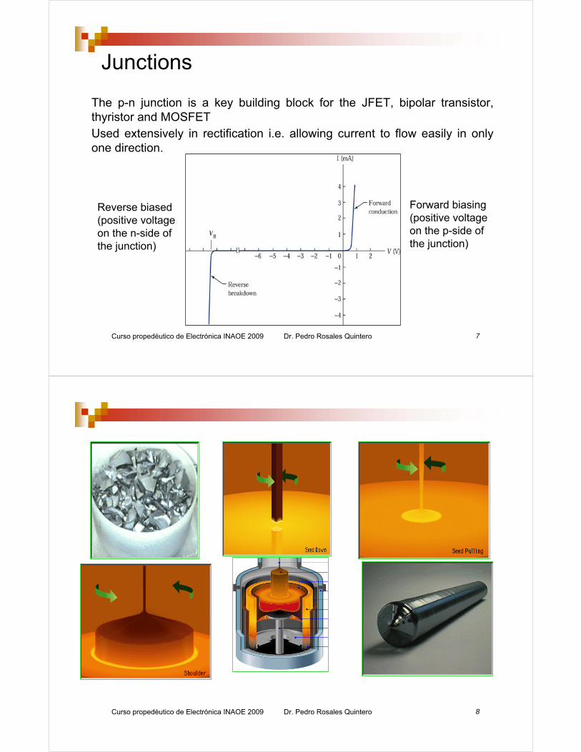
Junctions
The p-n junction is a key building block for the JFET, bipolar transistor, thyristor and MOSFETUsed extensively in rectification i.e. allowing current to flow easily in only one direction.
Forward biasing(positive voltage on the p-side of the junction)
Reverse biased(positive voltage on the n-side of the junction)
Curso propedéutico de Electrónica INAOE 2009 Dr. Pedro Rosales Quintero 8
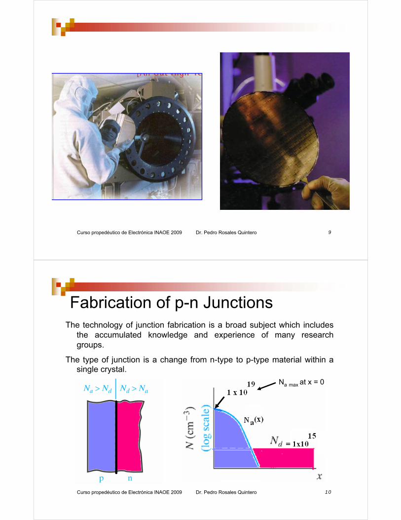
Curso propedéutico de Electrónica INAOE 2009 Dr. Pedro Rosales Quintero 9
Curso propedéutico de Electrónica INAOE 2009 Dr. Pedro Rosales Quintero 10
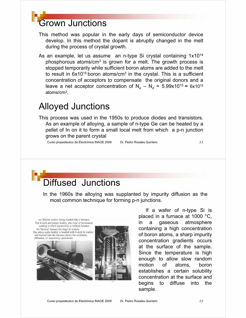
Fabrication of p-n JunctionsThe technology of junction fabrication is a broad subject which includes
the accumulated knowledge and experience of many research groups.
The type of junction is a change from n-type to p-type material within a single crystal.
Na max at x = 0
Curso propedéutico de Electrónica INAOE 2009 Dr. Pedro Rosales Quintero 11
Grown JunctionsThis method was popular in the early days of semiconductor device
develop. In this method the dopant is abruptly changed in the melt during the process of crystal growth.
As an example, let us assume an n-type Si crystal containing 1x10¹⁴
phosphorous atoms/cm3 is grown for a melt. The growth process is stopped temporarily while sufficient boron atoms are added to the melt to result in 6x10¹⁵ boron atoms/cm3 in the crystal. This is a sufficient concentration of acceptors to compensate the original donors and a leave a net acceptor concentration of Na – Nd = 5.99x10¹⁵ ≈ 6x10¹⁵
atoms/cm3.
Alloyed JunctionsThis process was used in the 1950s to produce diodes and transistors.
As an example of alloying, a sample of n-type Ge can be heated by a pellet of In on it to form a small local melt from which a p-n junction grows on the parent crystal
Curso propedéutico de Electrónica INAOE 2009 Dr. Pedro Rosales Quintero 12
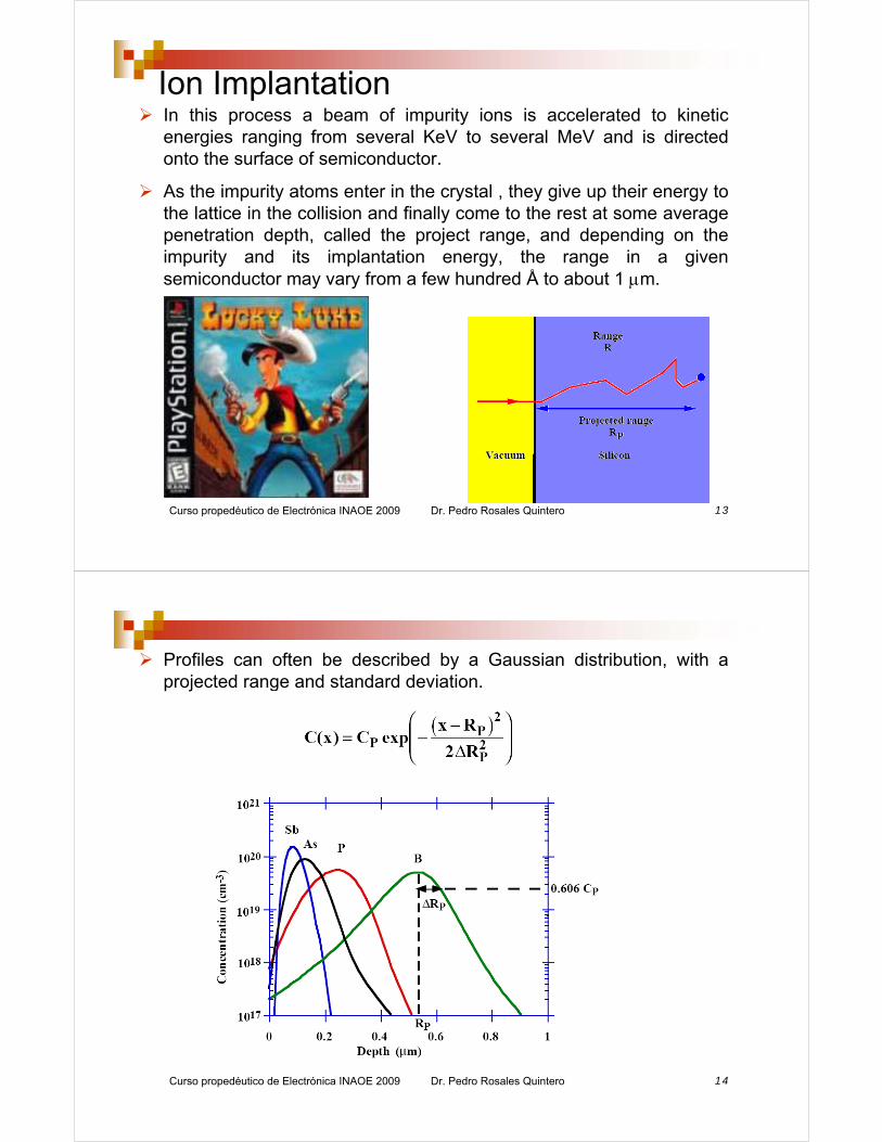
Diffused JunctionsIn the 1960s the alloying was supplanted by impurity diffusion as the
most common technique for forming p-n junctions.
If a wafer of n-type Si is placed in a furnace at 1000 °C, in a gaseous atmosphere containing a high concentration of boron atoms, a sharp impurity concentration gradients occurs at the surface of the sample. Since the temperature is high enough to allow slow random motion of atoms, boron establishes a certain solubility concentration at the surface and begins to diffuse into the sample.
Curso propedéutico de Electrónica INAOE 2009 Dr. Pedro Rosales Quintero 13
Ion ImplantationIn this process a beam of impurity ions is accelerated to kinetic energies ranging from several KeV to several MeV and is directed onto the surface of semiconductor.
As the impurity atoms enter in the crystal , they give up their energy to the lattice in the collision and finally come to the rest at some average penetration depth, called the project range, and depending on the impurity and its implantation energy, the range in a given semiconductor may vary from a few hundred Å to about 1 µm.
Curso propedéutico de Electrónica INAOE 2009 Dr. Pedro Rosales Quintero 14
Profiles can often be described by a Gaussian distribution, with a projected range and standard deviation.
Curso propedéutico de Electrónica INAOE 2009 Dr. Pedro Rosales Quintero 15
One of the major advantages is the precise control of the dopingconcentration.
One of the major problem with this doping method is the lattice damage, which results from collisions between the ions and the lattice atoms.
Curso propedéutico de Electrónica INAOE 2009 Dr. Pedro Rosales Quintero 16
Silicon Oxide
SiO2 and the Si/SiO2 interface are the principal reasons for
silicon’s dominance in the IC industry.
SiO2:
1. Easily selectively etched using lithography.
2. Masks most common impurities (B, P, As, Sb).
3. Excellent insulator (ρ > 1016 Ωcm, Eg > 9 eV).
4. High breakdown field (107 Vcm-1)
5. Stable bulk electrical properties.
6. Stable and reproducible interface with Si.
Curso propedéutico de Electrónica INAOE 2009 Dr. Pedro Rosales Quintero 17
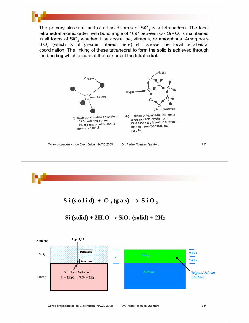
The primary structural unit of all solid forms of SiO2 is a tetrahedron. The local tetrahedral atomic order, with bond angle of 109° between O - Si - O, is maintained in all forms of SiO2 whether it be crystalline, vitreous, or amorphous. Amorphous SiO2 (which is of greater interest here) still shows the local tetrahedral coordination. The linking of these tetrahedral to form the solid is achieved through the bonding which occurs at the corners of the tetrahedral.
Curso propedéutico de Electrónica INAOE 2009 Dr. Pedro Rosales Quintero 18
S i (s o l i d) + O 2 (g a s) → S i O 2
Si (solid) + 2H2O → SiO2 (solid) + 2H2

Curso propedéutico de Electrónica INAOE 2009 Dr. Pedro Rosales Quintero 19
A temperatura ambiente, el silicio expuesto en un ambiente de oxígeno o aire, formará una capa de OXIDO NATIVO sobre la superficie de 5 – 10 Å en 5 min.
Curso propedéutico de Electrónica INAOE 2009 Dr. Pedro Rosales Quintero 20

Curso propedéutico de Electrónica INAOE 2009 Dr. Pedro Rosales Quintero 21
Today, the planar technology is used extensively for IC fabrication
Curso propedéutico de Electrónica INAOE 2009 Dr. Pedro Rosales Quintero 22
1. Introducción a Física Electrónica
1.1 Propiedades de cristales y crecimiento de semiconductores
1.2 Átomos y electrones
1.3 Bandas de energía y portadores de carga en semiconductores
1.4 Exceso de portadores en semiconductores
2. Uniones
2.1 Fabricación de uniones p-n
2.2 Condiciones de equilibrio
2.3 Polarización de uniones en directa e inversa bajo condiciones de estado estacionario
2.4 Ruptura bajo polarización inversa
2.5 Condiciones de transitorio y a-c
2.6 Desviaciones de la teoría sencilla
2.7 Uniones metal-semiconductor
TEMARIO DEL CURSO DE FUNDAMENTOS DE FÍSICA DE SEMICONDUCTORES

Curso propedéutico de Electrónica INAOE 2009 Dr. Pedro Rosales Quintero 23
1. Diagrama de bandas simplificado de un material semiconductor.
2. Portadores mayoritarios y minoritarios (dopado, neutralidad de carga, baja y alta inyección de portadores).
3. Mecanismos de transporte de portadores de carga.
4. Explique los procesos de recombinación indirecta e indirecta de portadores de carga.
5. ¿Qué representan las soluciones a la ecuación de continuidad? A continuación “describa físicamente” cada uno de los términos de la ecuación de continuidad.
6. ¿Qué es la longitud de difusión de los portadores de corriente?
7. ¿Qué es el tiempo de vida de recombinación de los portadores de corriente?
Curso propedéutico de Electrónica INAOE 2009 Dr. Pedro Rosales Quintero 24
Abrupt junction.The mathematics of p-n junctions is greatly simplified for the case of the step junction, which has uniform p doping on one side of the sharp junction and uniform doping in the other side. This model represents alloyed and epitaxial junctions quite well.
Curso propedéutico de Electrónica INAOE 2009 Dr. Pedro Rosales Quintero 25
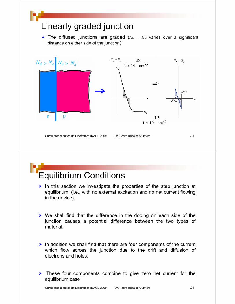
Linearly graded junctionThe diffused junctions are graded (Nd – Na varies over a significant distance on either side of the junction).
Curso propedéutico de Electrónica INAOE 2009 Dr. Pedro Rosales Quintero 26
Equilibrium ConditionsIn this section we investigate the properties of the step junction at equilibrium. (i.e., with no external excitation and no net current flowing in the device).
We shall find that the difference in the doping on each side of the junction causes a potential difference between the two types of material.
In addition we shall find that there are four components of the current which flow across the junction due to the drift and diffusion ofelectrons and holes.
These four components combine to give zero net current for the equilibrium case
Curso propedéutico de Electrónica INAOE 2009 Dr. Pedro Rosales Quintero 27
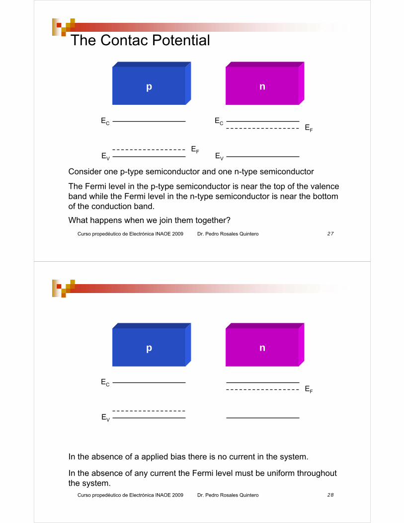
The Contac Potential
p n
EC
EV
EF
EC
EV
EF
Consider one p-type semiconductor and one n-type semiconductor
The Fermi level in the p-type semiconductor is near the top of the valence band while the Fermi level in the n-type semiconductor is near the bottom of the conduction band.
What happens when we join them together?
Curso propedéutico de Electrónica INAOE 2009 Dr. Pedro Rosales Quintero 28
p n
EC
EV
EF
In the absence of a applied bias there is no current in the system.
In the absence of any current the Fermi level must be uniform throughout the system.

Curso propedéutico de Electrónica INAOE 2009 Dr. Pedro Rosales Quintero 29
p n
EC
EV
EF
Large concentration gradients cause holes to diffuse from the p-side to the n-side and for electrons to diffuse from the n-side to the p-side…
+
-
diffusion
- electron+ hole
diffusion
Curso propedéutico de Electrónica INAOE 2009 Dr. Pedro Rosales Quintero 30
p n
EC
EV
EF
-
+
diffusion
diffusion
Eventually, charged donor & acceptor ions near the junction are left uncompensated and a negative space charge forms near the p-side and positive space charge near the n-side…this is known as the depletion region.
+ +
+ +
+ +
- -
- -
- -- Negative ion+ Positive ion

Curso propedéutico de Electrónica INAOE 2009 Dr. Pedro Rosales Quintero 31
-
p n
EC
EV
EF
-
+
diffusion
diffusion
The space charge region creates an electric field.
+ +
+ +
+ +
- -
- -
- -
+ drift
drift
Under the influence of the induced field, holes drift from the n-side to the p-side and electrons drift from the p-side to the n-side.
F
Curso propedéutico de Electrónica INAOE 2009 Dr. Pedro Rosales Quintero 32
To obtain a quantitative relationship between V0 and the doping concentrations on each side of the junction we must to use the requirements for equilibrium in the drift and diffusion current equations. For example:
( ) 0)(
)()( =⎥⎦⎤
⎢⎣⎡ −=
dx
xdpDxExpqxJ ppp µ
This equation can be rearranged and by using E(x)=-dV(x)/dx:
∫∫ =−n
p
p
p
Vn
Vp
dpp
dVq
kT 1

Curso propedéutico de Electrónica INAOE 2009 Dr. Pedro Rosales Quintero 33
We also derived an expression for the intrinsic carrier concentration,
(*)ln0 ⎟⎟⎠
⎞⎜⎜⎝
⎛=
n
p
p
p
q
kTV
law of mass action
Where nn and np are the electron densities in the n-type and p-type regions of the junction, the law of mass action tells us that,
2ippnn npnpn ==
⎟⎟⎠
⎞⎜⎜⎝
⎛=
20 lni
da
n
NN
q
kTV
So the built in voltage becomes,
⎟⎠⎞
⎜⎝⎛=
kT
qV
p
p
n
p 0exp
Another useful form for (*) is
Curso propedéutico de Electrónica INAOE 2009 Dr. Pedro Rosales Quintero 34
The depletion region
+
-
p-type n-type
-xp0 0 xn0
Let’s look closer at the depletion region,
We consider an abrupt junction with no applied bias,
We need to calculate the width of the depletion region,
00 np xxW +=
W
--
-
-
-
-
-
-
+++
+++
++
Curso propedéutico de Electrónica INAOE 2009 Dr. Pedro Rosales Quintero 35
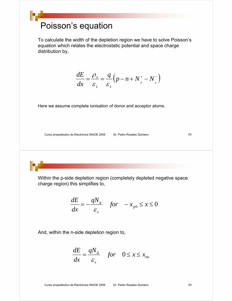
Poisson’s equation
To calculate the width of the depletion region we have to solve Poisson’s equation which relates the electrostatic potential and space charge distribution by,
Here we assume complete ionisation of donor and acceptor atoms.
( )−+ −+−==ad
NNnpq
dx
dE
ss
s
εερ
Curso propedéutico de Electrónica INAOE 2009 Dr. Pedro Rosales Quintero 36
Within the p-side depletion region (completely depleted negative space charge region) this simplifies to,
nos
d xxforqN
dx
dE≤≤= 0
ε
And, within the n-side depletion region to,
00 ≤≤−−= xxforqN
dx
dEp
s
a
ε

Curso propedéutico de Electrónica INAOE 2009 Dr. Pedro Rosales Quintero 37
Overall space charge neutrality requires,
00 ndpa xqANxqAN =
neutral p region neutral n region
-xp0 0 xn0
x
Nd
Na
+
-
depletion region
W
Curso propedéutico de Electrónica INAOE 2009 Dr. Pedro Rosales Quintero 38
At x=0 the two regions meet and the field is at its strongest, Emax
0x
-Emax
E
If we integrate to get the built in voltage,
s
nd
s
pa xqNxqNE
εε00
max −=−=
( ) WExqNxqN
dxxEVs
nod
x
x s
pan
p
max
220
0 2
1
22
0
0
=+== ∫− εε
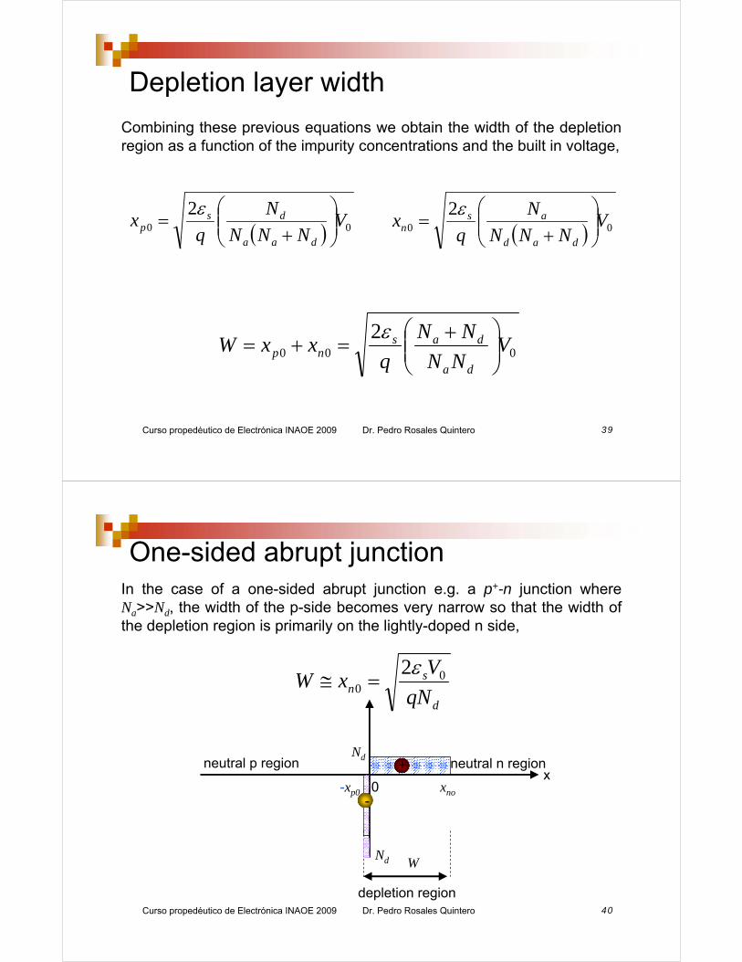
Depletion layer width
Area = V0 W
Curso propedéutico de Electrónica INAOE 2009 Dr. Pedro Rosales Quintero 39
Depletion layer width
000
2V
NN
NN
qxxW
da
dasnp ⎟⎟
⎠
⎞⎜⎜⎝
⎛ +=+=
ε
Combining these previous equations we obtain the width of the depletion region as a function of the impurity concentrations and the built in voltage,
( ) 00
2V
NNN
N
qx
daa
dsp ⎟⎟
⎠
⎞⎜⎜⎝
⎛+
=ε
( ) 00
2V
NNN
N
qx
dad
asn ⎟⎟
⎠
⎞⎜⎜⎝
⎛+
=ε
Curso propedéutico de Electrónica INAOE 2009 Dr. Pedro Rosales Quintero 40
One-sided abrupt junction
d
sn qN
VxW 0
0
2ε=≅
In the case of a one-sided abrupt junction e.g. a p+-n junction where Na>>Nd, the width of the p-side becomes very narrow so that the width of the depletion region is primarily on the lightly-doped n side,
neutral p region neutral n region
-xp0 0 xno
x
Nd
Nd
+
-
depletion region
W